Abstract
Among the various two-dimensional semiconductors, indium selenide has recently triggered the interest of scientific community, due to its band gap matching the visible region of the electromagnetic spectrum, with subsequent potential applications in optoelectronics and especially in photodetection. In this feature article, we discuss the main issues in the synthesis, the ambient stability and the application capabilities of this novel class of two-dimensional semiconductors, by evidencing open challenges and pitfalls. In particular, we evidence how the growth of single crystals with reduced amount of Se vacancies is crucial in the road map for the exploitation of indium selenide in technology through ambient-stable nanodevices with outstanding values of both mobility of charge carriers and ON/OFF ratio. The surface chemical reactivity of the InSe surface, as well as applications in the fields of broadband photodetection, flexible electronics and solar energy conversion are also discussed.
Keywords: indium selenide, exfoliation, Bridgman-Stockbarger growth, chemical reactivity, angle-resolved photoemission spectroscopy, nanodevices
1. Introduction
The recent interest toward layered semiconductors [1,2,3,4,5] is motivated by their potential impact in nanoelectronics [6,7,8,9], due to the joint presence of finite values of band gaps [10,11] and flexibility [12,13]. In particular, while graphene does not have a band gap [14,15,16,17], van der Waals semiconductors enable the devising of nanodevices with outstanding values for the ON/OFF ratio [6]. Moreover, by reducing the thickness, in some cases, the band gap becomes direct, with implications for optoelectronics [18] and photodetection.
Indium selenide represents an intriguing candidate for nanoelectronics [19], since it is an ambient-stable [20], flexible [21,22,23] semiconductor with high values of mobility of charge carriers [24]. Moreover, by exfoliating the bulk crystal, it is possible to attain nanosheets with a highly crystalline quality [25,26,27].
InSe is made of stacked layers of Se-In-In-Se atoms with van der Waals bonding between quadruple layers [28,29]. Recently, several researchers have reported the outstanding efficiency of InSe-based optoelectronic devices [30,31,32]. Field-effect transistors (FETs) with an active channel of few layers of InSe are characterized by values of electron mobility at room temperature as high as 103 cm2/(V·s) [30]. Furthermore, InSe has good prospects for applications in the field of photovoltaics [22], strain engineering [33], and nonlinear optics [34].
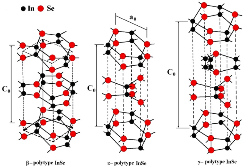
Depending on the different stacking sequences of layers, different polytypes of layered materials exist. Three highly distinct polytypes of the InSe crystal have been identified [35,36] (β, ε, and γ, see Figure 1), in which In and Se atoms are differently arranged. The β (space group symmetry ) and ε polytypes (space group symmetry ) are characterized by a hexagonal lattice consisting of eight atoms in the unit cell, and their extension over two layers [37]. Rhombohedral γ polytype (space group symmetry ) contains two cations and two anions distributed on four adjacent layers [35,38].
Figure 1.
Geometrical structure of the three polytypes of InSe. C0 and a0 represent the lattice parameters along the perpendicular to layers and in the layer plane, respectively. Reproduced from Ref. [39].
While ε-InSe has an indirect band gap of 1.4 eV [36], both β- and γ-InSe have a direct band gap [36] with closely matching values (1.28 eV [37] and 1.29 eV [40], respectively). Accordingly, only β and γ phases of InSe could supposedly be employed in optoelectronics, for which finite and direct band gaps are beneficial [41]. Exfoliated samples of γ-InSe host quantization effects, which enable near-infrared photoluminescence emission [26].
2. Growth
Several growth techniques have been used for growing indium-selenide compounds: vacuum evaporation [42], molecular beam epitaxy (MBE) [43], colloidal methods [44,45], flash evaporation [46], chemical vapour deposition [47], van der Waals epitaxy [48], radiofrequency sputtering [49], Czochralski [50] and the Bridgman-Stockbarger technique [37,51,52].
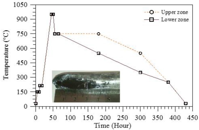
Among these methods, the Bridgman-Stockbarger growth is the most suitable for the large-scale production of high-quality bulk InSe semiconductors for device applications, with a typical time requirement ranging from 5 to 35 days for an ingot. The quite long time needed is also a consequence of some technical difficulties that need to be overcome during the growth process. The Bridgman-Stockbarger method involves starting from high-purity In and Se elements, which are sealed in quartz ampoules, heated in vacuum in a furnace at temperatures as high as 950 °C. Figure 2 shows the typical temperature profile at which the furnace should be kept during the growth process. However, selenium has a high vapor pressure value at temperatures higher than 600 °C [53], with possible fractures on the bulbs being used for growth. This problem can be avoided by decreasing the reaction rate, increasing the growth time, and/or by decreasing the growth temperature with a subsequent slower growth rate. Successively, the crucible is suspended in the middle of the vertical furnace with two designated zones. The temperature of the lower zone of the furnace is reduced to ~250 °C at a rate typically of around 1.5 °C/h. Both furnace zones are cooled to 250 °C over ~75 h. The solidified ingot is then cooled to room temperature over ~50 h.
Figure 2.
Temperature profile of the furnace in a typical Bridgman-Stockbarger growth of InSe single crystals [37]. In the inset an InSe single-crystal ingot grown by the Bridgman/Stockbarger method is displayed.
Using the Bridgman-Stockbarger method, InSe single crystals can be grown as both n- and p-type depending on growth conditions and dopant elements [54]. Doping can be achieved by the direct addition of the dopant elements to the growth ampoules [55,56,57,58,59,60,61,62,63,64,65,66,67]. To introduce dopants in a homogeneously distributed fashion, during the growth it is necessary to rotate the growth furnace, kept at about 50 °C above the melting point, around its own axis for many hours, at a particularly slow rate. In the choice of the dopant, one has to consider that the atomic radius of the doped elements should match that of the replaced atoms. In general, the grown crystals of InSe inevitably contain numerous defects, which act as deep trap levels. We reiterate that defects and impurities in semiconductors are associated with the energy levels in the forbidden gap. Thus, the presence of Se vacancies, i.e., anion vacancies, in InSe crystals leads to deep energy levels in the band gap. By doping InSe with transition metals, the localized levels originating from the vacancies disappear [37].
3. Exfoliation
The ingots of InSe, obtained by Bridgman-Stockberger technique, have no cracks and voids at the surface. Due to the extreme weakness of the interlayer van der Waals bond, the ingots can be easily cleaved along the (001) planes. Flakes with outstanding flatness and bright surfaces can be exfoliated from the parental bulk single-crystal ingot without chemical etching or mechanical polishing processes. To date, only mechanical exfoliation [23,26] (the ordinary scotch tape method) has been used to obtain atomically thick flakes of InSe. It is expected that liquid-phase exfoliation could be also achieved in future works on InSe. This achievement would boost the technological exploitation of InSe.
4. Electronic Properties
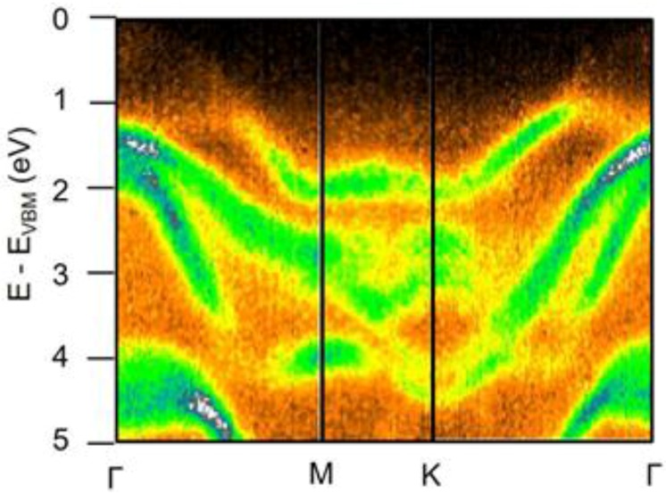
The electronic band structure of β-InSe has been measured by angle-resolved photoemission spectroscopy (ARPES) only in the case of bulk crystals [68] (Figure 3).
Figure 3.
Experimental band structure of β-InSe along the high-symmetry directions. The energy scale was set to zero at valence-band maximum (VBM). Reproduced with permission from Ref. [68].
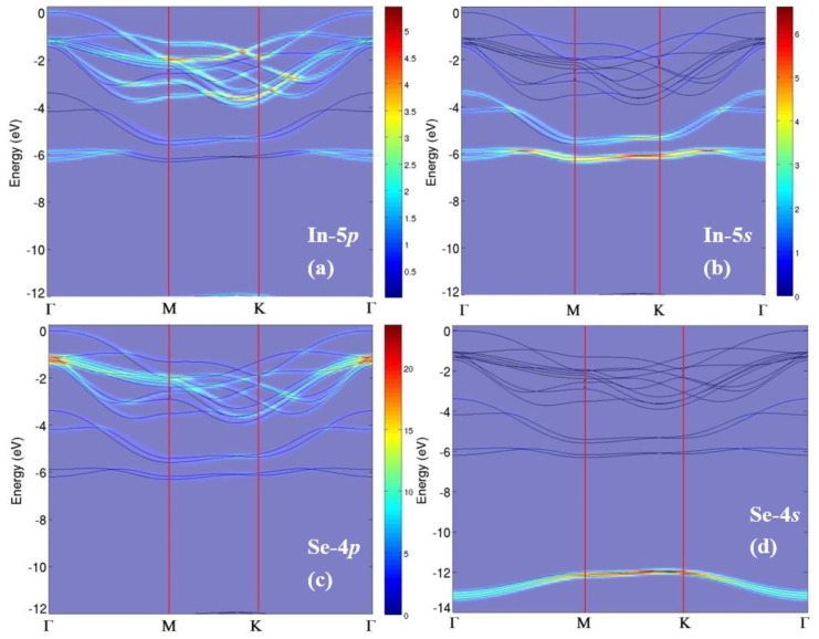
The orbital components of the different bands experimentally revealed by ARPES are indicated by projections to 5p (panel a of Figure 4) and 5s (panel b) states of In and to 4p (panel c) and 4s (panel d) states of Se along the whole Brillouin zone.
Figure 4.
Theoretical band structure projected to (a) In-5p; (b) In-5s; (c) Se-4p; and (d) Se-4s atomic orbitals. The intensity of the various bands is reported in a color scale, whose legend is displayed in the right part of panels (a,b) and between panels (c,d). Reproduced with permission from Ref. [68].
The valence-band maximum (VBM) is mainly derived from 5pz states of In. The crossing of bands at ~1.6 eV at Γ principally originates from the Se-4p and In-5s states, whereas states at 4.5 eV predominantly arise from In-5s.
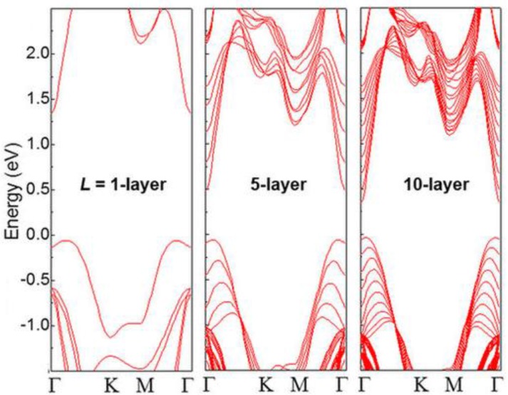
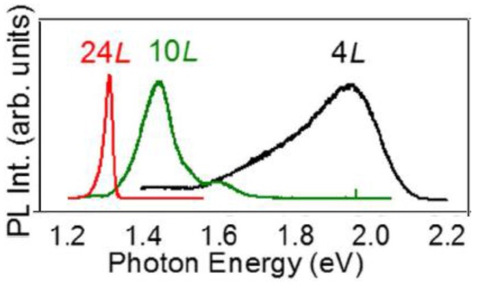
Concerning γ-InSe, density functional theory has evidenced a transition from direct to indirect band gap semiconductor, which occurs by reducing the number of layers [69], as also manifest from the analysis of Figure 5, where the behavior of the band structure of γ-InSe as a function of the thickness is shown. Figure 6 displays the dependence of the photoluminescence spectra, acquired with micrometric spatial resolution, as a function of thickness; by reducing the thickness, a shift of the maximum toward higher photon energies occurs.
Figure 5.
Band structure of γ-InSe with a number of layers L = 1, 5 and 10 layers. Reproduced with permission from Ref. [69].
Figure 6.
Normalized microphotoluminescence spectra for γ-InSe nanosheets with L = 4, 10 and 24 layers. Reproduced with permission from Ref. [69].
5. Ambient Stability
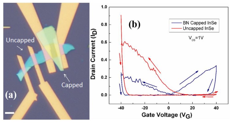
The stability of the performances of nanodevices in ambient conditions is an essential requisite in order to devise applications based on InSe. The ambient stability of FETs with an active channel of InSe has been demonstrated in Ref. [20]. However, therein, it was also shown that FETs with an active channel of uncapped InSe exhibit a p-type transport, while ambipolar transport was achieved only in the presence of a capping layer (Figure 7).
Figure 7.
(a) Optical image of typical InSe back-gate transistor devices: in one device the channel is capped with a flake of hexagonal boron nitride (h-BN), whereas the other channel is exposed to atmosphere. (b) Behavior of the drain current as a function of the gate voltage for the cases of capped and uncapped InSe-based transistors. The uncapped device shows dominant p-type transport (even if with notable hysteresis), while the capped device noticeably displays ambipolar transport. Reproduced with permission from Ref. [20]. Copyright Royal Society of Chemistry, 2016.
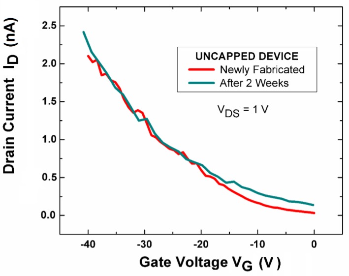
Nevertheless, even the uncapped InSe nanodevices are stable in air without any perceptible modification in the I-V curves measured again after two weeks (Figure 8). Consequently, one can affirm that no fast degradation occurs for InSe, contrary to the cases of Bi2Se3 [70] and black phosphorus [71].
Figure 8.
IDS-VG curve of uncapped InSe-based transistors freshly fabricated (red curve) and after two weeks (blue curve). Reproduced with permission from Ref. [20]. Copyright Royal Society of Chemistry, 2016.
For the case of InSe, the origin of the p-type doping of ambient-stable InSe-based FETs was unveiled in Ref. [20], where the authors investigated the correlation between the surface chemical reactivity, the environmental doping and the effects induced by defects in InSe (Figure 9).
Figure 9.
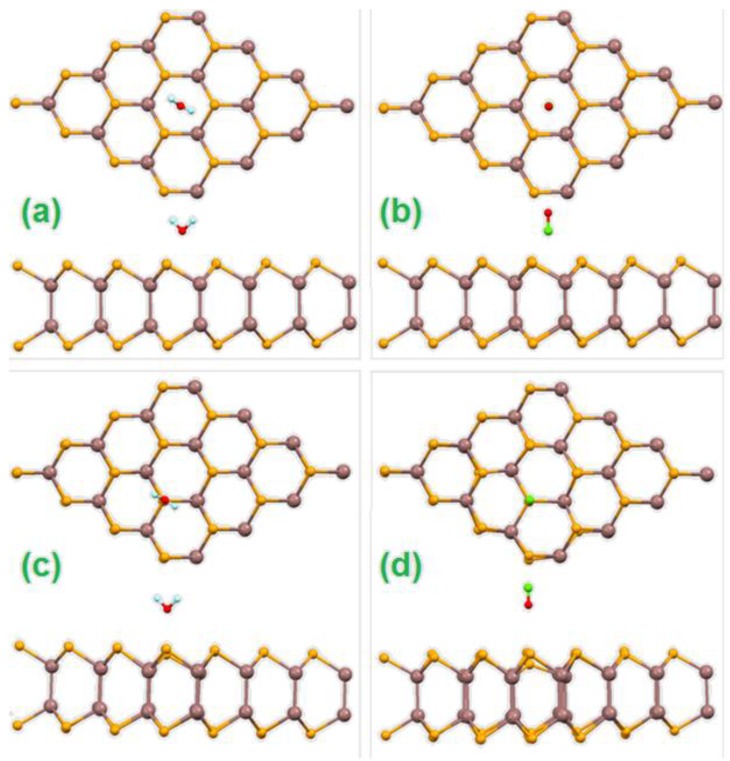
Top and side views of the geometrical structure of InSe monolayer in the case of adsorption of H2O (a,c) and CO (b,d) molecules over hole sites (a,b) and top sites (c,d) with respect to Se atoms. Reproduced with permission from Ref. [20]. Copyright Royal Society of Chemistry, 2016.
The interaction of ambient gases (H2O, CO, CO2, N2, O2) with InSe was assessed for two adsorption sites on undefected InSe: over Se atoms, which are the outermost surface atoms of the InSe monolayer (top position, Figure 9a,b), and over the middles of hexagons (hole position, Figure 9c,d). Theoretical results (Table 1) clarify that for all examined molecules the preferential adsorption site is that over holes.
Table 1.
Adsorption energies of different ambient species over the hole and on-top with respect to Se atoms. Reproduced with permission from Ref. [20]. Copyright Royal Society of Chemistry, 2016.
| Species/Adsorption Site | Hole (eV) | Top (eV) |
|---|---|---|
| H2O | −0.139 | 0.69 |
| CO | 0.014 | 2.75 |
| CO2 | 0.244 | 2.05 |
| N2 | 0.097 | 1.15 |
| O2 | 0.705 | 3.67 |
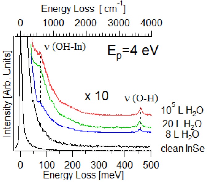
According to the values of adsorption energies calculated in Table 1, only the adsorption of H2O on hole sites is energetically favorable at room temperature, with a charge transfer of 0.01 electrons per each molecule. As a result, the InSe surface is only slightly p-doped. Therefore, among ambient gases, only water is able to form stable bonds with InSe at room temperature with manifest displacement of Se atoms from their positions in the pristine InSe (Figure 9c,d). These theoretical predictions have been confirmed by vibrational experiments, which also indicated that the adsorption of water molecules on InSe at room temperature is entirely dissociative. The vibrational spectrum of water-dosed InSe (Figure 10) exhibits an intense band at 450 meV, which constitutes a fingerprint of the water decomposition that occurred. As a matter of fact, this mode is due to the O–H stretching vibration in –OH groups [72], while molecular water would display O–H stretching energy in the 400–425 meV range [73].
Figure 10.
Vibrational spectrum of InSe exposed to water molecules at room temperature. Reproduced with permission from Ref. [20]. Copyright Royal Society of Chemistry, 2016.
Similarly, other recent theoretical works have recently reported positive adsorption energy of water molecules on Se vacancies [74] and almost zero adsorption energies for the physical adsorption of oxygen over various adsorption sites of the InSe surface [75]. Other theoretical works [76,77] Have reported rather large (0.1~0.3 eV) negative values of adsorption energies, but disagree with each other about type of doping from NH3 and about the values of the transferred charge from InSe substrate to molecules. In particular, results in Ref. [77] point to stable adsorption of molecules from air for all adsorption sites of InSe and, according to these theoretical predictions, InSe should be much more heavily doped under ambient conditions. However, it is quite evident that the theoretical model by Ma et al. [77] disagrees with experiments.
In InSe, extreme sensitivity of adsorption properties to local distortions is expected. Figure 9 depicts how adsorption on different sites provides different distortions of the atomic structure of InSe substrate. Molecular dynamic simulations also demonstrate the influence of the water layer on the structure of the InSe monolayer [78]. The optimization of both atomic positions and lattice constants provides a different magnitude of local distortions and, as a result, charge distribution, adsorption energies and charge transfer are subsequently modified.
It is worth reporting that two computational studies (both using the Vienna Ab initio simulation package- VASP- code) have recently reported contradictory results on the change of the lattice parameter when the InSe thickness is reduced down to the monolayer regime [79,80]. This disagreement between theoretical models highlights the noticeable dependence of results of the calculations on various usually unimportant and technical parameters. Moreover, the dependence of the energetics of adsorption from distortions permits the manipulation of chemical and electric properties of monolayer InSe by strain [32,77] or by distortion of scaffold, as previously reported for graphene [78,79]. Thickness-dependent changes of vibrational spectra of InSe [36] and GaSe [81] also prove the sensitivity of lattice properties of these compounds on the number of layers. Further theoretical investigation of the role of various substrates, ripples and strain on doping of InSe surface is ongoing.
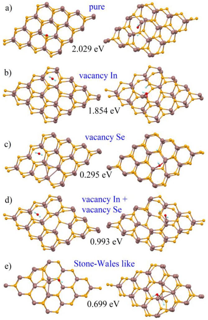
The calculation of the energy cost of dissociation of water molecules in both defect-free and defective InSe monolayer for the various kinds of defects (single In and Se vacancies, the combined existence of single In and Se vacancies, and Stone-Wales defects) indicates that water dissociation over undefected InSe is not energetically favored. In detail, the energetic cost is ~2 eV (Figure 11a). Analogously to the case of graphene [82], the presence of defects noticeably reduces the energy cost of chemisorption by a value depending on the type of defect. The presence of In vacancies reduces the energy cost for water decomposition to 1.85 eV (Figure 11b). Water decomposition is particularly favorable on Se vacancies, over which the energy cost is only 0.29 eV (Figure 11c). For the case of the joint presence of single In and Se vacancies, the energy cost for decomposition is about 1 eV (Figure 11d), while it is ~0.7 eV for the case of Stone-Wales defects (Figure 11e).
Figure 11.
Atomic structure of pristine (a) and defective (b–e) InSe monolayer before (left) and after (right) the decomposition of the water molecules. The indicated values represent the energy cost of the dissociation of water molecules for each specific case. Reproduced with permission from Ref. [20]. Copyright Royal Society of Chemistry, 2016.
Based on the relationship between calculated DFT energies and temperatures of reactions [83], it can be concluded that reactions with energies below 0.5 eV, e.g., in the case of water decomposition at Se vacancies, occur at room temperature at a rather high rate [20]. Calculations by Shi et al. [74] also indicate favorability of water decomposition on Se vacancies, and suggest a possible solution for this problem by reparation of the vacancies through substitution of missing Se atoms by S with a treatment of InSe surface in CH3SH. It is worth noticing that the substitution of Se with S and also the formation of local In2O3-like structures resulting from the penetration of oxygen atoms into the InSe monolayer [75] do not provide any visible changes in the band structure of InSe. These results suggest the routes toward healing of defects in InSe surfaces, but further modeling is required to find realistic methods.
6. Applications
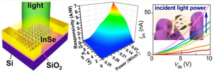
Compared with other group IIIA-VIA layered (MX, M = Ga and In, X = S, Se and Te), InSe has a narrower bandgap, which overlaps well with the solar spectrum and offers efficient solar energy conversion. Several works [84,85,86,87,88] have already demonstrated that InSe is an alternative candidate to thin-film cells, due to its high mechanical flexibility [21,23]. Tamalampudi et al. [23] have demonstrated that photodetectors with an active channel of a few layers of InSe show broadband efficiency from the visible to the near-infrared range (450–785 nm). InSe-based photodetectors have been fabricated on (i) a rigid SiO2/Si substrate, and (ii) a flexible polyethylene terephthalate (PET) film [23]. Photoresponsivities as high as 12.3 A·W−1 at 450 nm (on SiO2/Si) and 3.9 A·W−1 at 633 nm (on PET) have been measured [23], and with an order of magnitude improvement by simply sweeping the gate voltage above threshold of the transfer characteristic for electron conduction. The responsivity of InSe-based photodetectors in Figure 12 goes up to 7 A·W−1 at power intensity lower than 0.07 W·cm−2 (λ~633 nm), and this value is substantially higher than that of graphene- (5 × 10⁻⁴ A·W−1) and MoS2- (4.2 × 10⁻⁴ A·W−1) based photodetectors. Thus, InSe-based photodetectors are the most efficient among those realized with two-dimensional materials, including graphene and transition-metal dichalcogenides [7]. Their response time is only a few tens of ms and, moreover, they show long-term stability in photoswitching [23]. Remarkably, the bending of the InSe-based device fabricated on the flexible PET substrate does not significantly reduce its performances [23]. Therefore, the stretchable nature of InSe represents an ideal candidate for advanced optoelectronic applications.
Figure 12.
(left panel) Sketch of a InSe-based FETfor optoelectronics; (middle panel) Behavior of the responsivity as a function of the power and of the drain-source voltage; (right panel): The photocurrent of the InSe device on PET film (shown in the inset in the bent geometry) acquired when the device was in planar geometry with 633 nm illumination of 22.74, 8.67, 4.46, 2.85, 0.70, and 0.29 mW·cm−2 for purple, blue, green, yellow, orange, and red curves, respectively. Reproduced with permission from Ref. [23]. Copyright American Chemical Society, 2014.
With such excellent optoelectronic merits, layered InSe nanosheets will become not only outstanding candidates for optical sensing applications, but also promising components for configuring 2D heterostructure devices for high-performance photodetectors and emitters [89]. Owing to the low-density interface states, InSe-based hetero-junctions can be used for tailoring the device characteristics [90]. A graphene/few-layer InSe heterostructure photodetector has been reported with an external quantum efficiency of over 2 × 10⁵%, which represents a spectacular improvement with respect to the homostructural few-layer InSe device [32]. An absolute power conversion efficiency of about 18% for wavelengths of 1.10–1.25 µm has been reported for solar cells exploiting crystalline InSe as a window layer in heterostructure diodes [91]. Homojunction diodes formed from layers of p- and n-type InSe exhibit electroluminescence of exciton recombination at hν~1.23 eV. A ~20 meV redshift with respect to the photoluminance peak (1.25 eV) is observed. This redshift is attributed to the reabsorption of photons by the top InSe layer [92]. Conversely, heterojunction diodes formed by combining layers of p-type GaSe and n-type InSe emit photons at lower energies, due to the generation of spatially indirect excitons and a staggered valence band lineup for the holes at the GaSe/InSe interface [93].
Finally, in the prospect of a technological employment of atomically thin InSe nanosheets, it is worth mentioning that, by means of morphological nano-manipulation procedures such as nanotexturing, it is possible to enhance light absorption, bandwidth and the luminescent response [94].
7. Conclusions
In this feature article, we have discussed the main features of the science and technology based on InSe. Single crystals of InSe can be grown by different techniques, among which Bridgman-Stockbarger is the most suitable for up-scaling. As a matter of fact, it allows the production of large-scale, high-quality single crystals, which can be easily exfoliated to atomic thickness. To date, only mechanical exfoliation has been used, but we suggest that liquid-phase exfoliation would allow deeper employment of InSe in technology.
Nanodevices with flakes of InSe as active channels are characterized by high mobility of charge carriers and very high ON/OFF ratios. By reducing the thickness of the flakes, the band gap energy increases and a direct-to-indirect transition occurs, while electron and exciton effective masses are substantially constant with thickness. Concerning potential applications of InSe, highly performing broadband photodetectors and solar cells have been realized. The flexibility of InSe makes it a solid candidate for flexible electronics.
Ambient stability is one of the most valuable properties of InSe. However, the presence of Se vacancies enables water decomposition at room temperature, with the introduction of a p-type doping in InSe exposed to ambient air humidity. Therefore, the minimization of defects is the most important challenge in the growth of InSe compounds.
Author Contributions
The general structure of the Feature Article was conceived by Antonio Politano and Anna Cupolillo, who have also coordinated the various contributions. Each author has equally contributed to the draft taking in charge a part of the manuscript. In details, the paragraph on synthesis has been written by Bekir Gürbulak and Songül Duman. The section on electronic properties has been written by Anna Cupolillo, Antonio Politano, and Lorenzo S. Caputi. The paragraph on physical chemistry with InSe has been mostly written by Danil W. Boukhvalov, with contribution of Antonio Politano and Gennaro Chiarello for the review of existing vibrational studies. The paragraph on applications has been written by Lin Wang for InSe-based photodetectors and by Bekir Gürbulak and Songül Duman for InSe-based diodes.
Conflicts of Interest
The authors declare no conflict of interest.
References
- 1.Buscema M., Island J.O., Groenendijk D.J., Blanter S.I., Steele G.A., van der Zant H.S.J., Castellanos-Gomez A. Photocurrent generation with two-dimensional van der Waals semiconductors. Chem. Soc. Rev. 2015;44:3691–3718. doi: 10.1039/C5CS00106D. [DOI] [PubMed] [Google Scholar]
- 2.Roldán R., Castellanos-Gomez A., Cappelluti E., Guinea F. Strain engineering in semiconducting two-dimensional crystals. J. Phys. Condens. Matter. 2015;27 doi: 10.1088/0953-8984/27/31/313201. [DOI] [PubMed] [Google Scholar]
- 3.Scholz A., Stauber T., Schliemann J. Plasmons and screening in a monolayer of MoS2. Phys. Rev. B. 2013;88 doi: 10.1103/PhysRevB.88.035135. [DOI] [Google Scholar]
- 4.Stauber T., Gómez-Santos G. Plasmons in layered structures including graphene. New J. Phys. 2012;14 doi: 10.1088/1367-2630/14/10/105018. [DOI] [Google Scholar]
- 5.Lee T.H., Kim S.Y., Jang H.W. Black phosphorus: Critical review and potential for water splitting photocatalyst. Nanomaterials. 2016;6:194. doi: 10.3390/nano6110194. [DOI] [PMC free article] [PubMed] [Google Scholar]
- 6.Fiori G., Bonaccorso F., Iannaccone G., Palacios T., Neumaier D., Seabaugh A., Banerjee S.K., Colombo L. Electronics based on two-dimensional materials. Nat. Nanotechnol. 2014;9:768–779. doi: 10.1038/nnano.2014.207. [DOI] [PubMed] [Google Scholar]
- 7.Koppens F.H.L., Mueller T., Avouris P., Ferrari A.C., Vitiello M.S., Polini M. Photodetectors based on graphene, other two-dimensional materials and hybrid systems. Nat. Nanotechnol. 2014;9:780–793. doi: 10.1038/nnano.2014.215. [DOI] [PubMed] [Google Scholar]
- 8.Lee J.Y., Shin J.H., Lee G.H., Lee C.H. Two-dimensional semiconductor optoelectronics based on van der Waals heterostructures. Nanomaterials. 2016;6:193. doi: 10.3390/nano6110193. [DOI] [PMC free article] [PubMed] [Google Scholar]
- 9.Yang H., Qin S., Zheng X., Wang G., Tan Y., Peng G., Zhang X. An Al2O3 Gating Substrate for the Greater Performance of Field Effect Transistors Based on Two-Dimensional Materials. Nanomaterials. 2017;7:286. doi: 10.3390/nano7100286. [DOI] [PMC free article] [PubMed] [Google Scholar]
- 10.Miro P., Audiffred M., Heine T. An atlas of two-dimensional materials. Chem. Soc. Rev. 2014;43:6537–6554. doi: 10.1039/C4CS00102H. [DOI] [PubMed] [Google Scholar]
- 11.Bhimanapati G.R., Lin Z., Meunier V., Jung Y., Cha J., Das S., Xiao D., Son Y., Strano M.S., Cooper V.R., et al. Recent Advances in Two-Dimensional Materials beyond Graphene. ACS Nano. 2015;9:11509–11539. doi: 10.1021/acsnano.5b05556. [DOI] [PubMed] [Google Scholar]
- 12.Akinwande D., Petrone N., Hone J. Two-dimensional flexible nanoelectronics. Nat. Commun. 2014;5 doi: 10.1038/ncomms6678. [DOI] [PubMed] [Google Scholar]
- 13.Zhu W., Yogeesh M.N., Yang S., Aldave S.H., Kim J.-S., Sonde S., Tao L., Lu N., Akinwande D. Flexible Black Phosphorus Ambipolar Transistors, Circuits and AM Demodulator. Nano Lett. 2015;15:1883–1890. doi: 10.1021/nl5047329. [DOI] [PubMed] [Google Scholar]
- 14.Novoselov K. Graphene: Mind the gap. Nat. Mater. 2007;6:720–721. doi: 10.1038/nmat2006. [DOI] [PubMed] [Google Scholar]
- 15.Giubileo F., Di Bartolomeo A., Martucciello N., Romeo F., Iemmo L., Romano P., Passacantando M. Contact resistance and channel conductance of graphene field-effect transistors under low-energy electron irradiation. Nanomaterials. 2016;6:206. doi: 10.3390/nano6110206. [DOI] [PMC free article] [PubMed] [Google Scholar]
- 16.Luongo G., Giubileo F., Genovese L., Iemmo L., Martucciello N., Di Bartolomeo A. I-V and C-V Characterization of a High-Responsivity Graphene/Silicon Photodiode with Embedded MOS Capacitor. Nanomaterials. 2017;7:158. doi: 10.3390/nano7070158. [DOI] [PMC free article] [PubMed] [Google Scholar]
- 17.Jin K., Zhou X., Liu Z. Graphene/sulfur/carbon nanocomposite for high performance lithium-sulfur batteries. Nanomaterials. 2015;5:1481–1492. doi: 10.3390/nano5031481. [DOI] [PMC free article] [PubMed] [Google Scholar]
- 18.Wang X., Huang L., Peng Y., Huo N., Wu K., Xia C., Wei Z., Tongay S., Li J. Enhanced rectification, transport property and photocurrent generation of multilayer ReSe2/MoS2 p–n heterojunctions. Nano Res. 2015;9:507–516. doi: 10.1007/s12274-015-0932-6. [DOI] [Google Scholar]
- 19.Bandurin D.A., Tyurnina A.V., Yu G.L., Mishchenko A., Zolyomi V., Morozov S.V., Kumar R.K., Gorbachev R.V., Kudrynskyi Z.R., Pezzini S., et al. High electron mobility, quantum Hall effect and anomalous optical response in atomically thin InSe. Nat. Nanotechnol. 2017;12:223–227. doi: 10.1038/nnano.2016.242. [DOI] [PubMed] [Google Scholar]
- 20.Politano A., Chiarello G., Samnakay R., Liu G., Gurbulak B., Duman S., Balandin A.A., Boukhvalov D.W. The influence of chemical reactivity of surface defects on ambient-stable InSe-based nanodevices. Nanoscale. 2016;8:8474–8479. doi: 10.1039/C6NR01262K. [DOI] [PubMed] [Google Scholar]
- 21.Mosca D.H., Mattoso N., Lepienski C.M., Veiga W., Mazzaro I., Etgens V.H., Eddrief M. Mechanical properties of layered InSe and GaSe single crystals. J. Appl. Phys. 2002;91:140–144. doi: 10.1063/1.1423391. [DOI] [Google Scholar]
- 22.Ho C.-H., Chu Y.-J. Bending Photoluminescence and Surface Photovoltaic Effect on Multilayer InSe 2D Microplate Crystals. Adv. Opt. Mater. 2015;3:1750–1758. doi: 10.1002/adom.201500390. [DOI] [Google Scholar]
- 23.Tamalampudi S.R., Lu Y.Y., Kumar R., Sankar R., Liao C.D., Moorthy K., Cheng C.H., Chou F.C., Chen Y.T. High performance and bendable few-layered InSe photodetectors with broad spectral response. Nano Lett. 2014;14:2800–2806. doi: 10.1021/nl500817g. [DOI] [PubMed] [Google Scholar]
- 24.Ho P.-H., Chang Y.-R., Chu Y.-C., Li M.-K., Tsai C.-A., Wang W.-H., Ho C.-H., Chen C.-W., Chiu P.-W. High-Mobility InSe Transistors: The Role of Surface Oxides. ACS Nano. 2017;11:7362–7370. doi: 10.1021/acsnano.7b03531. [DOI] [PubMed] [Google Scholar]
- 25.Mudd G.W., Svatek S.A., Hague L., Makarovsky O., Kudrynskyi Z.R., Mellor C.J., Beton P.H., Eaves L., Novoselov K.S., Kovalyuk Z.D., et al. High Broad-Band Photoresponsivity of Mechanically Formed InSe–Graphene van der Waals Heterostructures. Adv. Mater. 2015;27:3760–3766. doi: 10.1002/adma.201500889. [DOI] [PMC free article] [PubMed] [Google Scholar]
- 26.Mudd G.W., Svatek S.A., Ren T., Patanè A., Makarovsky O., Eaves L., Beton P.H., Kovalyuk Z.D., Lashkarev G.V., Kudrynskyi Z.R., et al. Tuning the bandgap of exfoliated InSe nanosheets by quantum confinement. Adv. Mater. 2013;25:5714–5718. doi: 10.1002/adma.201302616. [DOI] [PMC free article] [PubMed] [Google Scholar]
- 27.Lin Z., Karthik P.S., Hada M., Nishikawa T., Hayashi Y. Simple technique of exfoliation and dispersion of multilayer graphene from natural graphite by ozone-assisted sonication. Nanomaterials. 2017;7:125. doi: 10.3390/nano7060125. [DOI] [PMC free article] [PubMed] [Google Scholar]
- 28.Sánchez-Royo J.F., Muñoz-Matutano G., Brotons-Gisbert M., Martínez-Pastor J.P., Segura A., Cantarero A., Mata R., Canet-Ferrer J., Tobias G., Canadell E., et al. Electronic structure, optical properties, and lattice dynamics in atomically thin indium selenide flakes. Nano Res. 2014;7:1556–1568. doi: 10.1007/s12274-014-0516-x. [DOI] [Google Scholar]
- 29.Ho C.-H. Thickness-dependent carrier transport and optically enhanced transconductance gain in III–VI multilayer InSe. 2D Mater. 2016;3 doi: 10.1088/2053-1583/3/2/025019. [DOI] [Google Scholar]
- 30.Sucharitakul S., Goble N.J., Kumar U.R., Sankar R., Bogorad Z.A., Chou F.-C., Chen Y.-T., Gao X.P.A. Intrinsic Electron Mobility Exceeding 103 cm2/(V·s) in Multilayer InSe FETs. Nano Lett. 2015;15:3815–3819. doi: 10.1021/acs.nanolett.5b00493. [DOI] [PubMed] [Google Scholar]
- 31.Lei S., Wen F., Ge L., Najmaei S., George A., Gong Y., Gao W., Jin Z., Li B., Lou J., et al. An Atomically Layered InSe Avalanche Photodetector. Nano Lett. 2015;15:3048–3055. doi: 10.1021/acs.nanolett.5b00016. [DOI] [PubMed] [Google Scholar]
- 32.Chen Z., Biscaras J., Shukla A. A high performance graphene/few-layer InSe photo-detector. Nanoscale. 2015;7:5981–5986. doi: 10.1039/C5NR00400D. [DOI] [PubMed] [Google Scholar]
- 33.Ma Y., Dai Y., Yu L., Niu C., Huang B. Engineering a topological phase transition in β-InSe via strain. New J. Phys. 2013;15 doi: 10.1088/1367-2630/15/7/073008. [DOI] [Google Scholar]
- 34.Yüksek M., Yaglioglu H.G., Elmali A., Aydin E.M., Kürüm U., Ateş A. Nonlinear and saturable absorption characteristics of Ho doped InSe crystals. Opt. Commun. 2014;310:100–103. doi: 10.1016/j.optcom.2013.07.078. [DOI] [Google Scholar]
- 35.Han G., Chen Z.-G., Drennan J., Zou J. Indium Selenides: Structural Characteristics, Synthesis and Their Thermoelectric Performances. Small. 2014;10:2747–2765. doi: 10.1002/smll.201400104. [DOI] [PubMed] [Google Scholar]
- 36.Lei S., Ge L., Najmaei S., George A., Kappera R., Lou J., Chhowalla M., Yamaguchi H., Gupta G., Vajtai R., et al. Evolution of the Electronic Band Structure and Efficient Photo-Detection in Atomic Layers of InSe. ACS Nano. 2014;8:1263–1272. doi: 10.1021/nn405036u. [DOI] [PubMed] [Google Scholar]
- 37.Gürbulak B., Şata M., Dogan S., Duman S., Ashkhasi A., Keskenler E.F. Structural characterizations and optical properties of InSe and InSe: Ag semiconductors grown by Bridgman/Stockbarger technique. Physica E. 2014;64:106–111. doi: 10.1016/j.physe.2014.07.002. [DOI] [Google Scholar]
- 38.Mudd G.W., Patanè A., Kudrynskyi Z.R., Fay M.W., Makarovsky O., Eaves L., Kovalyuk Z.D., Zólyomi V., Falko V. Quantum confined acceptors and donors in InSe nanosheets. Appl. Phys. Lett. 2014;105 doi: 10.1063/1.4903738. [DOI] [Google Scholar]
- 39.Zhirko Y., Trachevsky V., Kovalyuk Z. Hydrogen Storage. InTech; Rijeka, Croatia: 2012. On the Possibility of Layered Crystals Application for Solid State Hydrogen Storages—InSe and GaSe Crystals. [Google Scholar]
- 40.Julien C.M., Balkanski M. Lithium reactivity with III–VI layered compounds. Mater. Sci. Eng. B. 2003;100:263–270. doi: 10.1016/S0921-5107(03)00113-2. [DOI] [Google Scholar]
- 41.Viti L., Hu J., Coquillat D., Knap W., Tredicucci A., Politano A., Vitiello M.S. Black Phosphorus Terahertz Photodetectors. Adv. Mater. 2015;27:5567–5572. doi: 10.1002/adma.201502052. [DOI] [PubMed] [Google Scholar]
- 42.El-Sayed S. Optical investigations of the indium selenide glasses. Vacuum. 2003;72:169–175. doi: 10.1016/S0042-207X(03)00139-8. [DOI] [Google Scholar]
- 43.Emery J.Y., Brahim-Ostmane L., Hirlimann C., Chevy A. Reflection high-energy electron diffraction studies of InSe and GaSe layered compounds grown by molecular beam epitaxy. J. Appl. Phys. 1992;71:3256–3259. doi: 10.1063/1.350972. [DOI] [Google Scholar]
- 44.Lauth J., Kulkarni A., Spoor F.C.M., Renaud N., Grozema F.C., Houtepen A.J., Schins J.M., Kinge S., Siebbeles L.D.A. Photogeneration and Mobility of Charge Carriers in Atomically Thin Colloidal InSe Nanosheets Probed by Ultrafast Terahertz Spectroscopy. J. Phys. Chem. Lett. 2016;7:4191–4196. doi: 10.1021/acs.jpclett.6b01835. [DOI] [PubMed] [Google Scholar]
- 45.Lauth J., Gorris F.E.S., Samadi Khoshkhoo M., Chassé T., Friedrich W., Lebedeva V., Meyer A., Klinke C., Kornowski A., Scheele M., et al. Solution-Processed Two-Dimensional Ultrathin InSe Nanosheets. Chem. Mater. 2016;28:1728–1736. doi: 10.1021/acs.chemmater.5b04646. [DOI] [Google Scholar]
- 46.Julien C., Samaras I., Tsakiri M., Dzwonkowski P., Balkanski M. Lithium insertion in InSe films and applications in microbatteries. Mater. Sci. Eng. B. 1989;3:25–29. doi: 10.1016/0921-5107(89)90174-8. [DOI] [Google Scholar]
- 47.Park J.-H., Afzaal M., Helliwell M., Malik M.A., O’Brien P., Raftery J. Chemical vapor deposition of indium selenide and gallium selenide thin films from mixed alkyl/dialkylselenophosphorylamides. Chem. Mater. 2003;15:4205–4210. doi: 10.1021/cm0310420. [DOI] [Google Scholar]
- 48.Lang O., Klein A., Schlaf R., Löher T., Pettenkofer C., Jaegermann W., Chevy A. InSeGaSe heterointerfaces prepared by Van der Waals epitaxy. J. Cryst. Growth. 1995;146:439–443. doi: 10.1016/0022-0248(94)00504-4. [DOI] [Google Scholar]
- 49.Shigetomi S., Ikari T. Crystalline InSe films prepared by RF-sputtering technique. Jpn. J. Appl. Phys. 1991;30:L2127. doi: 10.1143/JJAP.30.L2127. [DOI] [Google Scholar]
- 50.Chevy A., Gouskov A., Besson J. Growth of crystalline slabs of layered InSe by the Czochralski method. J. Cryst. Growth. 1978;43:756–759. doi: 10.1016/0022-0248(78)90157-4. [DOI] [Google Scholar]
- 51.De Blasi C., Micocci G., Mongelli S., Tepore A. Large InSe single crystals grown from stoichiometric and non-stoichiometric melts. J. Cryst. Growth. 1982;57:482–486. doi: 10.1016/0022-0248(82)90062-8. [DOI] [Google Scholar]
- 52.Chevy A. Improvement of growth parameters for Bridgman-grown InSe crystals. J. Cryst. Growth. 1984;67:119–124. doi: 10.1016/0022-0248(84)90140-4. [DOI] [Google Scholar]
- 53.Hoshino H., Schmutzler R.W., Hensel F. The High Temperature Vapour Pressure Curve and the Critical Point of Liquid Selenium. Ber. Bunsenges. Phys. Chem. 1976;80:27–31. doi: 10.1002/bbpc.19760800108. [DOI] [Google Scholar]
- 54.Shigetomi S., Ikari T. Electrical and optical properties of n- and p-InSe doped with Sn and As. J. Appl. Phys. 2003;93:2301–2303. doi: 10.1063/1.1539558. [DOI] [Google Scholar]
- 55.Duman S., Elkoca Z., Gurbulak B., Bahtiyari Tekle T., Dogan S. Metal/p-InSe:Mn Schottky barrier diodes. J. Optoelectron. Adv. Mater. 2012;14:693–698. [Google Scholar]
- 56.Duman S., Gürbulak B., Doǧan S., Türüt A. Electrical characteristics and inhomogeneous barrier analysis of Au–Be/p-InSe:Cd Schottky barrier diodes. Microelectron. Eng. 2009;86:106–110. doi: 10.1016/j.mee.2008.10.004. [DOI] [Google Scholar]
- 57.Duman S., Gurbulak B., Turut A. Temperature-dependent optical absorption measurements and Schottky contact behavior in layered semiconductor n-type InSe(:Sn) Appl. Surf. Sci. 2007;253:3899–3905. doi: 10.1016/j.apsusc.2006.08.018. [DOI] [Google Scholar]
- 58.Gürbulak B., Kundakçi M., Ateş A., Yildirim M. Electric field influence on exciton absorption of Er doped and undoped InSe single crystals. Phys. Scr. 2007;75:424–430. doi: 10.1088/0031-8949/75/4/008. [DOI] [Google Scholar]
- 59.Gürbulak B. Urbach tail and optical investigations of Gd doped and undoped InSe single crystals. Phys. Scr. 2004;70:197–201. doi: 10.1088/0031-8949/70/2-3/020. [DOI] [Google Scholar]
- 60.Ateş A., Yildirim M., Gürbulak B. Investigation of the electrical properties of Ho-doped InSe single crystal. Physica E. 2004;21:85–90. doi: 10.1016/j.physe.2003.08.074. [DOI] [Google Scholar]
- 61.Shigetomi S., Ikari T. Impurity levels in layered semiconductor n-InSe doped with Ge. Phys. Status Solidi B. 2003;236:135–142. doi: 10.1002/pssb.200301558. [DOI] [Google Scholar]
- 62.Shigetomi S., Ikari T. Optical and Electrical Characteristics of Layered Semiconductor p-InSe Doped with Sb. Jpn. J. Appl. Phys. Part 1. 2003;42:6951–6954. doi: 10.1143/JJAP.42.6951. [DOI] [Google Scholar]
- 63.Shigetomi S., Ikari T. Optical and electrical properties of layer semiconductor n-InSe doped with Sn. Jpn. J. Appl. Phys. Part 1. 2002;41:5565–5566. doi: 10.1143/JJAP.41.5565. [DOI] [Google Scholar]
- 64.Shigetomi S., Ikari T. Annealing behavior of layer semiconductor p-InSe doped with Hg. Jpn. J. Appl. Phys. Part 1. 2000;39:1184–1185. doi: 10.1143/JJAP.39.1184. [DOI] [Google Scholar]
- 65.Gürbulak B., Yildirim M., Ateç A., Doǧan S., Yoǧurtçu Y.K. Growth and Temperature Dependence of Optical Properties of Er Doped and Undoped n-Type InSe. Jpn. J. Appl. Phys. Part 1. 1999;38:5133–5136. doi: 10.1143/JJAP.38.5133. [DOI] [Google Scholar]
- 66.Gürbulak B. Growth and optical properties of Dy doped and undoped n-type InSe single crystal. Solid State Commun. 1999;109:665–669. doi: 10.1016/S0038-1098(98)00613-9. [DOI] [Google Scholar]
- 67.Shigetomi S., Ikari T., Nakashima H. Impurity levels in p-type layered semiconductor InSe doped with Hg. Phys. Status Solidi B. 1998;209:93–99. doi: 10.1002/(SICI)1521-3951(199809)209:1<93::AID-PSSB93>3.0.CO;2-Z. [DOI] [Google Scholar]
- 68.Politano A., Campi D., Cattelan M., Ben Amara I., Jaziri S., Mazzotti A., Barinov A., Gürbulak B., Duman S., Agnoli S., et al. Indium selenide: An insight on electronic band structure and surface excitations. Sci. Rep. 2017;7 doi: 10.1038/s41598-017-03186-x. [DOI] [PMC free article] [PubMed] [Google Scholar]
- 69.Mudd G.W., Molas M.R., Chen X., Zólyomi V., Nogajewski K., Kudrynskyi Z.R., Kovalyuk Z.D., Yusa G., Makarovsky O., Eaves L., et al. The direct-to-indirect band gap crossover in two-dimensional van der Waals Indium Selenide crystals. Sci. Rep. 2016;6 doi: 10.1038/srep39619. [DOI] [PMC free article] [PubMed] [Google Scholar]
- 70.Kong D., Cha J.J., Lai K., Peng H., Analytis J.G., Meister S., Chen Y., Zhang H.J., Fisher I.R., Shen Z.X., Cui Y. Rapid surface oxidation as a source of surface degradation factor for Bi2Se3. ACS Nano. 2011;5:4698–4703. doi: 10.1021/nn200556h. [DOI] [PubMed] [Google Scholar]
- 71.Island J.O., Steele G.A., van der Zant H.S.J., Castellanos-Gomez A. Environmental instability of few-layer black phosphorus. 2D Mater. 2015;2 doi: 10.1088/2053-1583/2/1/011002. [DOI] [Google Scholar]
- 72.Politano A., Chiarello G. Enhancement of hydrolysis in alkali ultrathin layers on metal substrates in the presence of electron confinement. Chem. Phys. Lett. 2010;494:84–87. doi: 10.1016/j.cplett.2010.05.089. [DOI] [Google Scholar]
- 73.Henderson M.A. The interaction of water with solid surfaces: Fundamental aspects revisited. Surf. Sci. Rep. 2002;46:1–308. doi: 10.1016/S0167-5729(01)00020-6. [DOI] [Google Scholar]
- 74.Shi L., Zhou Q., Zhao Y., Ouyang Y., Ling C., Li Q., Wang J. Oxidation mechanism and protection strategy of ultrathin Indium Selenide: Insight from Theory. J. Phys. Chem. Lett. 2017;8:4368–4373. doi: 10.1021/acs.jpclett.7b02059. [DOI] [PubMed] [Google Scholar]
- 75.Xiao K., Carvalho A., Neto A.C. Defects and oxidation resilience in InSe. Phys. Rev. B. 2017;96 doi: 10.1103/PhysRevB.96.054112. [DOI] [Google Scholar]
- 76.Cai Y., Zhang G., Zhang Y.-W. Charge Transfer and Functionalization of Monolayer InSe by Physisorption of Small Molecules for Gas Sensing. J. Phys. Chem. C. 2017;121:10182–10193. doi: 10.1021/acs.jpcc.7b02286. [DOI] [Google Scholar]
- 77.Ma D., Ju W., Tang Y., Chen Y. First-principles study of the small molecule adsorption on the InSe monolayer. Appl. Surf. Sci. 2017;426:244–252. doi: 10.1016/j.apsusc.2017.07.198. [DOI] [Google Scholar]
- 78.Peng Q., Xiong R., Sa B., Zhou J., Wen C., Wu B., Anpo M., Sun Z. Computational mining of photocatalysts for water splitting hydrogen production: Two-Dimensional InSe-family monolayers. Catal. Sci. Technol. 2017;7:2744–2752. doi: 10.1039/C7CY00090A. [DOI] [Google Scholar]
- 79.Guo Y., Zhou S., Bai Y., Zhao J. Enhanced piezoelectric effect in Janus group-III chalcogenide monolayers. Appl. Phys. Lett. 2017;110:163102. doi: 10.1063/1.4981877. [DOI] [Google Scholar]
- 80.Jin H., Li J., Dai Y., Wei Y. Engineering the electronic and optoelectronic properties of InX (X = S, Se, Te) monolayers via strain. Phys. Chem. Chem. Phys. 2017;19:4855–4860. doi: 10.1039/C6CP08158D. [DOI] [PubMed] [Google Scholar]
- 81.Quan L., Song Y., Lin Y., Zhang G., Dai Y., Wu Y., Jin K., Ding H., Pan N., Luo Y. The Raman enhancement effect on a thin GaSe flake and its thickness dependence. J. Mater. Chem. C. 2015;3:11129–11134. doi: 10.1039/C5TC02209F. [DOI] [Google Scholar]
- 82.Boukhvalov D.W., Katsnelson M.I. Chemical Functionalization of Graphene with Defects. Nano Lett. 2008;8:4373–4379. doi: 10.1021/nl802234n. [DOI] [PubMed] [Google Scholar]
- 83.Boukhvalov D.W., Dreyer D.R., Bielawski C.W., Son Y.-W. A Computational Investigation of the Catalytic Properties of Graphene Oxide: Exploring Mechanisms by using DFT Methods. ChemCatChem. 2012;4:1844–1849. doi: 10.1002/cctc.201200210. [DOI] [Google Scholar]
- 84.Gordillo G., Calderón C. CIS thin film solar cells with evaporated InSe buffer layers. Sol. Energy Mater. Sol. Cells. 2003;77:163–173. doi: 10.1016/S0927-0248(02)00319-7. [DOI] [Google Scholar]
- 85.Segura A., Chevy A., Guesdon J.P., Besson J.M. Photovoltaic efficiency of InSe solar cells. Sol. Energy Mater. 1979;2:159–165. doi: 10.1016/0165-1633(79)90015-7. [DOI] [Google Scholar]
- 86.Damodara Das V., Sathyanarayanan J., Damodare L. Effect of annealing and surface treatment on the efficiency of photoelectrochemical (PEC) solar cells with vacuum-deposited n-InSe thin film electrode. Surf. Coat. Technol. 1997;94–95:669–671. [Google Scholar]
- 87.Kovalyuk Z., Katerynchuk V., Savchuk A., Sydor O. Intrinsic conductive oxide–p-InSe solar cells. Mater. Sci. Eng. B. 2004;109:252–255. doi: 10.1016/j.mseb.2003.10.074. [DOI] [Google Scholar]
- 88.Darwish A., Hanafy T., Attia A., Habashy D., El-Bakry M., El-Nahass M. Optoelectronic performance and artificial neural networks (ANNs) modeling of n-InSe/p-Si solar cell. Superlattices Microstruct. 2015;83:299–309. doi: 10.1016/j.spmi.2015.03.033. [DOI] [Google Scholar]
- 89.Mandal K.C., Das S. Fabrication and characterization of improved p-GaTe/n-InSe heterojunction solar cells; Proceedings of the 2012 38th IEEE Photovoltaic Specialists Conference (PVSC); Austin, TX, USA. 3–8 June 2012; pp. 000177–000180. [Google Scholar]
- 90.Mönch W. Semiconductor Surfaces and Interfaces. Volume 26. Springer; Berlin, Germany: 2013. Interface States; pp. 81–103. [Google Scholar]
- 91.Ando K., Katsui A. Optical properties and photovoltaic device applications of InSe films. Thin Solid Films. 1981;76:141–148. doi: 10.1016/0040-6090(81)90245-5. [DOI] [Google Scholar]
- 92.Balakrishnan N., Kudrynskyi Z.R., Fay M.W., Mudd G.W., Svatek S.A., Makarovsky O., Kovalyuk Z.D., Eaves L., Beton P.H., Patanè A. Room Temperature Electroluminescence from Mechanically Formed van der Waals III-VI Homojunctions and Heterojunctions. Adv. Opt. Mater. 2014;2:1064–1069. doi: 10.1002/adom.201400202. [DOI] [Google Scholar]
- 93.Chen X.B., Kelley D.F. Photophysics of GaSe/InSe nanoparticle heterojunctions. J. Phys. Chem. B. 2006;110:25259–25265. doi: 10.1021/jp064477u. [DOI] [PubMed] [Google Scholar]
- 94.Brotons-Gisbert M., Andres-Penares D., Suh J., Hidalgo F., Abargues R., Rodríguez-Cantó P.J., Segura A., Cros A., Tobias G., Canadell E. Nanotexturing to enhance photoluminescent response of atomically thin indium selenide with highly tunable band gap. Nano Lett. 2016;16:3221–3229. doi: 10.1021/acs.nanolett.6b00689. [DOI] [PubMed] [Google Scholar]


