

Abstract
Water absorption was studied in two types of waveguides made from unannealed plasma enhanced chemical vapor deposition (PECVD) SiO2. Standard rib anti-resonant reflecting optical waveguides (ARROWs) were fabricated with thin films of different intrinsic stress and indices of refraction. Buried ARROWs (bARROWs) with low and high refractive index differences between the core and cladding regions were also fabricated from the same types of PECVD films. All waveguides were subjected to a heated, high humidity environment and their optical throughput was tested over time. Due to water absorption in the SiO2 films, the optical throughput of all of the ARROWs decreased with time spent in the wet environment. The ARROWs with the lowest stress SiO2 had the slowest rate of throughput change. High index difference bARROWs showed no decrease in optical throughput after 40 days in the wet environment and are presented as a solution for environmentally stable waveguides made from unannealed PECVD SiO2.
Index Terms: Silica, optical waveguides, integrated optics, microfabrication, intrinsic film stress, water absorption
I. Introduction
OPTOFLUIDICS and integrated optics make use of integrated optical waveguides fabricated using microfabrication processes in order to manipulate light and engineer useful devices. These fields continue to push the envelope, developing new technologies that outperform and replace older macro devices. For example, optofluidics is producing lab-on-a-chip biosensors that are capable of probing aqueous samples for individual bioparticles [1]–[4].
These new technologies rely on low loss optical waveguides that must be made using stable, high quality, and low optical absorbing materials in order to perform acceptably. SiO2 is one of the most popular materials for making integrated optical waveguides in the visible regime, especially SiO2 that is deposited using plasma enhanced chemical vapor deposition (PECVD) [5], [6]. There are many advantages to using PECVD SiO2 including low deposition temperatures (∼250°C), conformal depositions, relatively fast deposition rates, precise control of the film’s index of refraction, and ease of use. It is well known, however, that SiO2 grown using PECVD will readily absorb water from the atmosphere, which can cause critical material property changes post fabrication [7], [8]. A common solution to prevent this is to simply anneal the SiO2 at high temperatures (>900°C) post deposition, which helps densify the SiO2 and makes it more impervious to water absorption. This solution is not viable when other materials or components within a device will not stand up to such high temperature cycling without significant damage occurring. In such temperature sensitive cases a device designer is compelled to use unannealed SiO2 and face the problem of water absorption which can cause unpredictable changes in device performance post fabrication.
An important example of such undesired changes is the reported significant decrease in optical throughput, as high as a 90% decrease, of standard rib anti-resonant reflecting optical waveguides (ARROWs) with time spent in a wet environment [9], [10]. These studies concluded that these significant transmission losses were not due to increased optical absorption in the hydrated film, but that the decrease occurs due to changes in the index of refraction profile of the ARROW. The index of refraction of the SiO2 increases as the film absorbs water from its surroundings and as water absorbs deeper into the film, it creates an undesired high index layer at the surface of the waveguide. The presence of this high index layer causes optical power to couple out of the guiding core, leading to high optical power loss. It should be noted that these effects also occur in normal atmospheric conditions, but are expedited when the waveguides are left in a heated and high humidity environment.
In this letter SiO2 ARROWs were tested with time spent in a wet environment in order to investigate the effect of intrinsic film stress and index of refraction on water absorption in unannealed PECVD SiO2 films. Intrinsic stress of the SiO2 film making up the waveguides was identified as a major factor affecting the degree of water absorption in the film. Despite optimizing the stress in attempts to eliminate water absorption, water absorption was not completely eliminated in these films.
Because water absorption cannot be completely eliminated in unannealed PECVD SiO2 films, this letter presents and tests a solution for waveguides that is independent of water absorption. The solution relies on a buried ARROW (bARROW) design with high index of refraction contrast between the core and cladding layers. The optical throughput of these bARROWs was also tested versus time in a wet environment and was shown to have no decrease in throughput after 40 days exposure.
II. Study on Film Stress and Water Absorption
A. Film Stress and Refractive Index Tuning in PECVD
One advantage of PECVD is the ability to precisely tune and manipulate the intrinsic film stress and refractive index of the deposited film. One of the more basic methods to alter these values is by simply altering the flow rates of the source gases, silane (SiH4) and nitrous oxide (N2O), which causes predictable changes in both film stress and refractive index [11]. Adding a dopant gas source, such as CF4, also affects the index of refraction and intrinsic stress of the film [12], [13]. A combination of both of these methods was used in order to fabricate the different waveguides used in this experiment.
Fig. 1 shows a graph of the index of refraction and film stress versus CF4 flow rate in the PECVD chamber (Oxford Instruments PlasmaLab80Plus) that was used to grow all of the SiO2 films used in this study. The solid lines represent index of refraction and the dashed lines indicate the film stress. The index of refraction measurements were made using a manual, 635 nm wavelength ellipsometer (Gaertner 1169-AK) and the stress values were measured using an optical profilometer (Zeta 20). It is clear in Fig. 1 that the addition of the CF4 gas source generally caused the index of refraction of the SiO2 film to decrease, while causing the intrinsic stress in the film to become more positive or tensile. Conversely, increasing the SiH4/N2O ratio caused the index of refraction to increase.
Fig. 1.
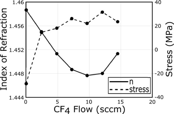
Graph showing relationship between index of refraction and film stress versus CF4 flow rate. The SiH4 to N2O flow rate ratio was kept constant during these growths at 0.152. All depositions were done at 250°C.
B. ARROW Fabrication
ARROWs were fabricated on silicon substrates using standard microfabrication procedures. First, six ARROW layers were sputtered directly onto the silicon wafer. These layers were alternating SiO2 and Ta2O5 layers whose thicknesses and indices of refraction were designed to provide an optical buffer between the ARROW core and the silicon substrate underneath [14]–[16]. Using the methods described in the above section on film stress and refractive index tuning in PECVD, 6 μm thick SiO2 films were deposited on top of these ARROW layers with various stress and index of refraction values. All of the oxides studied in this letter were deposited at 250°C and the details of their process recipes are included in Table I. An etch mask was then patterned over the SiO2 core layer using standard photolithography techniques in order to define 4 μm wide ribs. These ribs were etched into the SiO2 film to a height of 3 μm using an anisotropic RIE/ICP dry etcher (Trion Phantom III) and afterwards the etch mask was removed. Fig. 2(a) shows an SEM image of a completed ARROW.
TABLE I.
Process Recipes for Various Oxides in this Letter
| Recipe | HF (W) |
LF (W) |
Si4 (sccm) |
N2O (sccm) |
CF4 (sccm) |
Pressure (mtorr) |
|---|---|---|---|---|---|---|
| −50 Stress |
40 | 20 | 170 | 710 | 0 | 1500 |
| 0* Stress |
16 | 0 | 164 | 88 | 0 | 1900 |
| +50 Stress |
25 | 0 | 164 | 88 | 0 | 1900 |
| +100** Stress |
16 | 0 | 164 | 88 | 40 | 1900 |
| LID Core |
36 | 0 | 82 | 34.2 | 0 | 1100 |
| LID Cladding |
36 | 0 | 82 | 34.2 | 9.6 | 1100 |
The 0 stress recipe was also used for the HID bARROW core.
The +100 stress recipe was used for the HID bARROW cladding
Fig. 2.
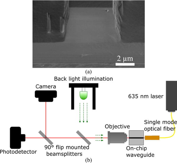
(a) SEM image of a ±0 stress ARROWs. (b) Optical setup used for testing the optical throughput of the waveguides.
C. Water Absorption Testing
Immediately after fabrication, the ARROWs were subjected to a 12 hour 300°C bake, in order to ensure the absence of any water in the SiO2 waveguides. This bake-out procedure has been shown to be effective for driving absorbed water from SiO2 thin films [10]. The waveguides were then characterized using the optical testing setup shown in Fig. 2(b). This setup allowed for the accurate manual alignment of waveguides to a single mode optical fiber in order to measure their optical power throughput. Back light illumination was used to focus on the mode profile of the waveguides to ensure correct alignment. A 635 nm, single mode laser (Thorlabs S1FC635) was used for all measurements in this experiment.
Afterwards, the waveguides were subjected to a heated and high humidity (wet) environment for an extended period of time. The temperature in the wet environment was 60°C and the relative humidity was measured at 99%. The waveguides were periodically removed from the wet environment and recharacterized on the optical testing setup. The waveguides were also visibly inspected throughout the experiment using an optical microscope and no physical damage was discovered.
D. Results: Water Absorption vs. Film Stress
Fig. 3 shows the results of the optical throughput testing. A decrease in optical throughput over time corresponds to water absorption that has occurred in the SiO2 films.
Fig. 3.
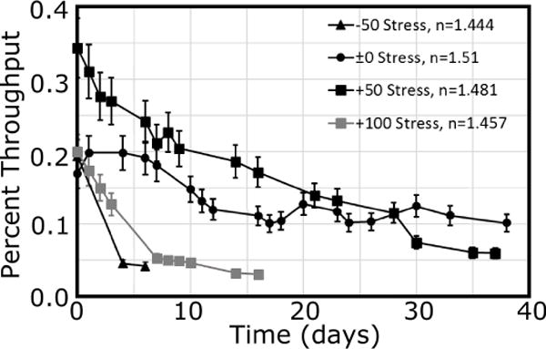
Average percent optical throughput vs. the time the ARROWs spent in the wet environment. The ±0 MPa ARROWs are shown with a solid black line and circles. The −50 MPa ARROWs are shown with a solid black line and triangles. The +50 and +100 ARROWs both have squares and are shown with a solid black line and a solid grey line, respectively.
The ±0 MPa stress ARROWs were the most resilient, decreasing by only 50% after nearly 40 days of testing. The −50 MPa stress ARROWs performed very poorly with time in the wet environment. After only a few days the optical throughput dropped dramatically. The +50 MPa and +100 MPa ARROWs decreased in optical throughput slower than the −50 MPa ARROWs. It took 10 full days for the +50 MPa ARROWs to drop to only 50% their original value; however, the throughput continued to drop and by day 40 the optical throughput had decreased by a full 80% of the original value. Note that the throughput on day 0 was different for each waveguide due to several factors including: variations in the fabrication process, the quality of the cleaved facets, and variations in the coupling efficiency because the waveguides possess different refractive indices.
It is important to note that we attempted to manipulate only the stress of the oxide films; however, our results indicate that the index of refraction of the films was lower for films with higher stress. Because low index values may indicate a more porous, or air filled, film, this could also indicate that higher porosity films are more absorptive. However, the porosity of the films was not specifically evaluated in this study.
III. Buried ARROW Structure
While the results of the wet environment testing on the SiO2 films indicate that the ±0 MPa stress ARROWs had the lowest decrease in optical throughput with time spent in the wet environment, all the waveguides exhibited throughput loss. We thus concluded that water absorption occurred in all of the unannealed PECVD films. To mitigate this problem, a high index difference buried ARROW waveguide (bARROW) is introduced and studied under similar conditions. This structure has already been investigated and reported to reduce the effects of water absorption in unannealed PECVD SiO2, however, the bARROWs tested in that experiment still experienced a significant decrease in optical throughput (~50%) after 20 days in a wet environment [9]. Those earlier studies relied on a low index difference bARROW structure which were still susceptible to a loss of modal guiding as refractive indices changed with water absorption.
Fig. 4(a) shows an SEM image of a bARROW. The earlier bARROWs that experienced a 50% decrease in optical throughput had ncore = 1.48 and nclad = 1.46. It has been reported that the index of refraction of a film increases by as much as 1.8% with the incorporation of water into the film [17]. If the cladding layer in this initial bARROW were to increase by 1.8%, its new index value would be 1.486, which is higher than the refractive index of the core. This new high index layer will cause optical power to couple out of the core, resulting in higher loss.
Fig. 4.
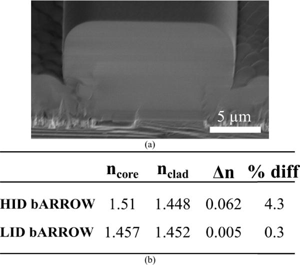
(a) SEM image of a buried ARROW waveguide fabricated and tested in this study. (b) Index of refraction values for HID and LID bARROWs.
If the difference between ncore and nclad were made to be much larger than the 1.8% increase expected due to water absorption in the film, then the waveguiding structure would be much less affected by changes in refractive index due to water absorption in the cladding film.
Analysis also shows that high index of refraction contrast between the core and cladding layers of a waveguide leads to small modes, confined to the core of the waveguide, while low index contrast leads to larger modes that extend into the cladding layer, making these waveguides more susceptible to changes near the surface of the cladding layer.
High index difference (HID) and low index difference (LID) bARROW structures were designed, fabricated, and tested. These waveguides were fabricated using a very similar procedure as that described above for making the ARROWs. First, ARROW layers were deposited on a silicon substrate in order to provide an optical buffer between the waveguide core and the high index silicon substrate. Next, a 4 μm thick PECVD SiO2 layer (ncore) was deposited directly on top of the ARROW layers. The channels were etched into this SiO2 layer and finally, a 6 μm thick PECVD SiO2 cladding layer (nclad) was grown over the channels. Fig. 4(b) shows the different refractive index values of these layers and the Δn for each bARROW design.
The HID and LID bARROWs were both tested using the same procedure as the ARROWs. Fig. 5 shows the results of the HID and LID bARROW testing. After almost 40 days in the wet environment the HID bARROWs still maintained a high percent optical throughput, while the LID bARROWs had almost no optical power throughput after less than 10 days in the same wet environment. This demonstrates that increasing the index contrast in the bARROW made with unannealed PECVD SiO2 greatly enhances its environmental stability. This occurs because the index difference between the core and the cladding layers is large enough that nclad cannot be driven above ncore by water absorption. The value of nclad of the HID BARROW was measured to be 1.448. This means, the expected index of refraction would only be 1.474 after water absorption. The index of refraction (ncore) of the core SiO2 is well above this value at an index of 1.51.
Fig. 5.
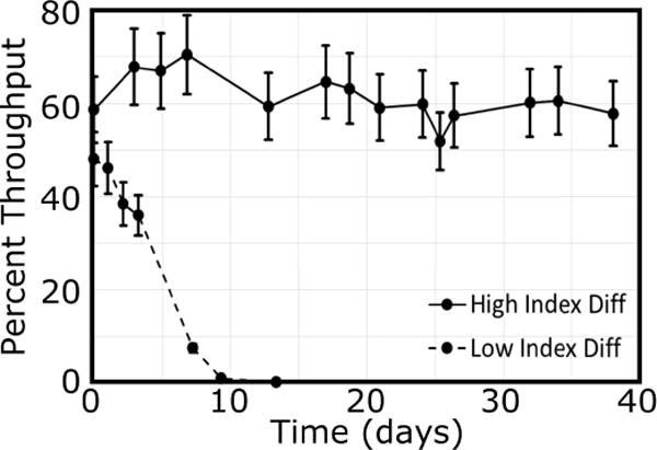
Average percent optical throughput vs. the time the bARROWs spent in the wet environment. The solid black line represents the HID bARROWs and the dashed line shows the data for the LID bARROWs.
In comparison, the index of refraction of the cladding layer of the LID waveguides is 1.452 and would expect to increase to as high as 1.478 after water absorption occurs in the layer. That change in the index of refraction of the cladding layer creates a top layer in the cladding with a higher index of refraction than that of the guiding core at 1.457. As water absorption progresses, this layer diffuses closer to the core and eventually the high index top layer begins to couple power out of the core and into the lossy high index top layer, destroying the waveguiding capability of the bARROW.
IV. Conclusion
The results of the ARROW testing indicate that although keeping film stress as low as possible in unannealed PECVD SiO2 helps limit the amount of water absorption that occurs within the film, it does not eliminate the problem entirely. It is clear that all unannealed PECVD SiO2 films will absorb some water and the effects cannot be ignored when using these films for waveguiding. One way to maximize the environmental stability of unannealed PECVD SiO2 waveguides is the use of a HID bARROW design. This bARROW design showed an excellent ability to resist any decrease in optical power throughput due to water absorption from the environment.
Footnotes
Color versions of one or more of the figures in this letter are available online at http://ieeexplore.ieee.org.
Contributor Information
Thomas Wall, Department of Electrical and Computer Engineering, Brigham Young University, Provo, UT 84602 USA.
Steven Hammon, Department of Electrical and Computer Engineering, Brigham Young University, Provo, UT 84602 USA.
Erik Hamilton, Department of Electrical and Computer Engineering, Brigham Young University, Provo, UT 84602 USA.
Gabriel Zacheu, Department of Electrical and Computer Engineering, Brigham Young University, Provo, UT 84602 USA.
Marcos Orfila, Department of Electrical and Computer Engineering, Brigham Young University, Provo, UT 84602 USA.
Holger Schmidt, School of Engineering, University of Californnia at Santa Cruz, Santa Cruz, CA 95064 USA.
Aaron R. Hawkins, Department of Electrical and Computer Engineering, Brigham Young University, Provo, UT 84602 USA
References
- 1.Ozcelik D, et al. Optofluidic wavelength division multiplexing for single-virus detection. Proc Nat Acad Sci USA. 2015 Sep;112(42):12933–12937. doi: 10.1073/pnas.1511921112. [DOI] [PMC free article] [PubMed] [Google Scholar]
- 2.Cai H, et al. Optofluidic analysis system for amplification-free, direct detection of Ebola infection. Sci Rep. 2015 Sep;5:14494. doi: 10.1038/srep14494. [DOI] [PMC free article] [PubMed] [Google Scholar]
- 3.Cho SH, Godin JM, Chen CH, Qiao W, Lee H, Lo YH. Review article: Recent advancements in optofluidic flow cytometer. Biomicrofluidics. 2010 Dec;4(4):043001. doi: 10.1063/1.3511706. [DOI] [PMC free article] [PubMed] [Google Scholar]
- 4.Godin J, Chen C-H, Cho SH, Qiao W, Tsai F, Lo Y-H. Microfluidics and photonics for bio-system-on-a-chip: A review of advancements in technology towards a microfluidic flow cytometry chip. J Biophoton. 2008 Oct;1(5):355–376. doi: 10.1002/jbio.200810018. [DOI] [PMC free article] [PubMed] [Google Scholar]
- 5.Grand G, Jadot JP, Denis H, Valette S, Fournier A, Grouillet AM. Low-loss pecvd silica channel wave-guides for optical communications. Electron Lett. 1990 Dec;26(25):2135–2137. [Google Scholar]
- 6.Ou H. Different index contrast silica-on-silicon waveguides by PECVD. Electron Lett. 2003 Jan;39(2):212–213. [Google Scholar]
- 7.McInerney EJ, Flinn PA. Diffusivity of moisture in thin films. Proc 20th Annu Rel Phys Symp. 1982 Apr;:264–267. [Google Scholar]
- 8.Riera M, Rodríguez JA, Barreto J, Domínguez C. Modeling of non-stoichiometric silicon oxides obtained by plasma enhanced chemical vapour deposition process. Solid Films. 2007 Feb;515(7–8):3380–3386. [Google Scholar]
- 9.Wall TA, Chu RP, Parks JW, Ozcelik D, Schmidt H, Hawkins AR. Improved environmental stability for plasma enhanced chemical vapor deposition SiO2 waveguides using buried channel designs. Opt Eng. 2016 Apr;55(4):040501. doi: 10.1117/1.OE.55.4.040501. [DOI] [PMC free article] [PubMed] [Google Scholar]
- 10.Parks J, Cai H, Wall T, Hawkins AR, Schmidt H. Enhancement of ARROW photonic device performance via thermal annealing of PECVD-based SiO2 waveguides. IEEE J Sel Topics Quantum Electron. 2016 Nov;22(6):249–254. doi: 10.1109/JSTQE.2016.2549801. [DOI] [PMC free article] [PubMed] [Google Scholar]
- 11.Lai Q, Gu JS, Smit MK, Schmid J, Melchior H. Simple technologies for fabrication of low-loss silica waveguides. Electron Lett. 1992 May;28(11):1000–1001. [Google Scholar]
- 12.Bulat ES, et al. Fabrication of waveguides using low-temperature plasma processing techniques. J Vac Sci Technol A, Vac Surf Films. 1993 Feb;11(4):1268–1274. [Google Scholar]
- 13.Tabasky M, Bulat ES, Tweed B, Herrick C. Investigation of thick, low-temperature plasma deposited silica films for waveguide fabrication. J Vac Sci Technol A, Vac Surf Films. 1994 Mar;12(4):1244–1251. [Google Scholar]
- 14.Yin D, Deamer DW, Schmidt H, Barber JP, Hawkins AR. Integrated optical waveguides with liquid cores. Appl Phys Lett. 2004 Aug;85(16):3477–3479. [Google Scholar]
- 15.Yin DL, Lunt EJ, Rudenko MI, Deamer DW, Hawkins AR, Schmidt H. Planar optofluidic chip for single particle detection, manipulation, and analysis. Lab Chip. 2007 Jun;7(9):1171–1175. doi: 10.1039/b708861b. [DOI] [PubMed] [Google Scholar]
- 16.Zhao Y, et al. Tailoring the spectral response of liquid waveguide diagnostic platforms. J Biophoton. 2012 Aug;5(8–9):703–711. doi: 10.1002/jbio.201200049. [DOI] [PMC free article] [PubMed] [Google Scholar]
- 17.Stott M, et al. Silicate spin-on-glass as an overcoat layer for SiO2 ridge waveguides. Proc CLEO, San Jose, CA, USA. 2015 May; paper JTh2A.29.D. [Google Scholar]