Abstract
Graphene has several unique physical, optical and electrical properties such as a two-dimensional (2D) planar structure, high optical transparency and high carrier mobility at room temperature. These make graphene interesting for electrical biosensing. Using a catalyst-free chemical vapor deposition (CVD) method, graphene film is grown on a sapphire substrate. There is a single or a few sheets as confirmed by Raman spectroscopy and atomic force microscopy (AFM). Electrical graphene biosensors are fabricated to detect large-sized biological analytes such as cancer cells. Human colorectal carcinoma cells are sensed by the resistance change of an active bio-functionalized graphene device as the cells are captured by the immobilized antibody surface. The functionalized sensors show an increase in resistance as large as ~20% of the baseline with a small number of adhered cells. This study suggests that the bio-functionalized electrical graphene sensors on sapphire, which is a highly transparent material, can potentially detect circulating tumor cells (CTCs) and monitor cellular electrical behavior while being compatible with fluorescence-based optical-detection bioassays.
Keywords: Biosensors, Graphene, 2D, Cell Detection, CVD
1. INTRODUCTION
Graphene, a two-dimensional (2D) single or a few sheets of sp2-hybridized carbon atoms, exhibits exceptional material properties such as high intrinsic carrier mobility, semi-metallic property, high optical transparency and high surface area-to-mass ratio at room temperature.1–5 In addition, graphene may be a better alternative to overcome various problems commonly observed in carbon nano-tube (CNT) structures. For instance, it is difficult to manipulate CNTs for device fabrication if only a few of them are used.6, 7 A 2D planar structure of graphene allows for simpler device process and more complex integration using established semiconductor processes. Additionally, its high Young’s modulus and optical transparency are remarkably useful in fabricating competent optical devices and sensors for nanoelectromechanical systems (NEMS).4,8, 9 As it exhibits unique and attractive properties, graphene is potentially a useful nanomaterial for biological and chemical sensor development in various applications.10–13 Demonstrations include detection of gases,14 pH,15 cells,16–18 bacteria,19 and biomolecules such as glucose, DNA, and protein.13, 20–24 Graphene-based biosensors, for example, have shown their advantages such as improved detection sensitivity due to high surface area-to-volume ratio, unique optical properties, and ease of effective surface modification.25–27
Here, we describe a simple, label-free electrical resistance-based detection of cancer cells for potential applications of monitoring cellular electrical behavior28–31 by using bio-functionalized graphene on a sapphire substrate. A single or a few nanosheets of high-quality graphene film is grown using a catalyst-free chemical vapor deposition (CVD) method, which is later confirmed by Raman spectroscopy and atomic force microscopy (AFM).32 Fabricated using traditional micro-fabrication technology, the electrical graphene biosensors are structurally simple with size-controlled sensing graphene surface and are easily operated without presence of solution-gate. The mechanism of sensor action is involved with human colorectal carcinoma cells being captured by the immobilized active EpCAM (Epithelial Cell Adhesion Molecule) antibody-coated graphene surface layer, resulting in conductance change. Having applied low electric fields to avoid any damage of cancer cells or degradation of biological analytes, the functionalized microsensors exhibit change in resistance as large as ~20% of its baseline with a small number of captured cells.
2. EXPERIMENTAL DETAILS
2.1. Graphene Growth and Device Fabrication
Electrical biosensors are fabricated using CVD-grown graphene film on a sapphire substrate. To eliminate complex transfer processes, graphene is directly grown on sapphire substrate without any metal catalyst using high temperature van der Waal’s epitaxy technique. A 0.43 mm thick c-plane (0001) double sided polished sapphire wafer (MTI corp.) is used for graphene growth without any chemical or thermal pre-treatment of the wafer. Substrate temperature initially increases to 1000 °C at a rate of 100 °C/min and reaches its final growth temperature (1350 °C to 1650 °C) at 250 °C/min. Ar, the main carrier gas, is introduced into the growth chamber with a flow rate of ~10,000 sccm during outgassing and the chamber pressure is kept at 600 Torr. Most of hydrocarbon gases can be applied for high temperature graphene synthesis but methane is preferably used for higher quality film growth. Hydrogen plays an important role since it controls the growth rate. The optimal hydrogen to methane flow ratio is determined to be about 10. Alignment marks are first patterned by a contact aligner and etched using RF oxygen plasma for a minute and aluminum oxide RIE (reactive-ion etching) (BCl3: 30 sccm, Ar: 20 sccm) for about an hour to etch graphene and sapphire, respectively. Afterwards we pattern the graphene nanosheet and briefly apply RF oxygen plasma etch again to define active channel regions of the sensors. The active graphene channels are 100 μm long and 10 or 20 μm wide. To form drain and source metal contacts (100×100 μm2), 10 nm thick titanium and 200 nm thick gold are deposited onto both ends of the patterned square graphene region (100 ×100 μm2) by an electron-gun evaporator.
2.2. Surface Functionalization
The bio-functionalization of CVD-grown graphene surface prior to antibody immobilization is performed by the following order:
MPTMS (3-Mercaptopropyltrimethoxysilane) is deposited onto the graphene region using molecular vapor deposition (MVD) (MVD100E, Applied MicroStructures) for 15 minutes. It is important not to perform RF O2 pre-clean before running the process to prevent any damage of the graphene film.
GMBS (N-g-maleimidobutyryloxy succinimide ester) (Cat. # 22309, Thermo Scientific) solution is applied to the MPTMS-functionalized surface with 30 minutes of incubation and washed with ethanol.
NeutrAvidin (Cat. # 31000, Thermo Scientific) dissolved in 1 × PBS (phosphate buffered saline) is prepared for the subsequent functionalization step and 1 hour incubation is allowed, followed by the PBS wash. And
biotinylated EpCAM antibody (Cat. #, BAF960, R&D Systems) is introduced to the NeutrAvidin-functionalized surface. Its concentration is at 15 μm/ml dissolved in 1× PBS with 1% (w/v) BSA (bovine serum albumin) and 0.01% (w/v) sodium azide. BSA and sodium azide are used to prevent non-specific hydrophobic binding and to preserve the antibodies for longer time, respectively. To remove access EpCAM antibody, the antibody-coated surface is washed with 1× PBS after 1 hour incubation.
2.3. Cell Culture and Preparation
HCT116 cells are cultured in McCoy’s 5A (Life Technologies) with 10% FBS (fetal bovine serum) and 1% P/S (penicillin-streptomycin) solution. The cells are washed with 1× PBS, trypsinized to detach them from the plate and collected in a centrifuge tube. After the cells (~1×10⁶ cells per ml) are suspended, 4% PFA is applied in the tube on nice for 10 minutes to fix the cells. Subsequently, the cells are washed with 1× PBS and re-suspended in 1× PBS containing 1% (w/v) BSA and 2 mM EDTA (ethylenediaminetetraacetic acid) solution. After cells, the biological analyte for this study, are added onto the EpCAM antibody-coated surface, the device is incubated for 1 hour and washed with 1× PBS.
2.4. Sensor Measurements
In order to measure its electrical characteristics, each electrical biosensor is connected to a commercial precision semiconductor parameter analyzer (Agilent 4165c) with a probe station. DC voltage source is connected between drain and source metal contacts, which is swept from 0 to 500 mV with an incremental step of 10 mV, and DC output current is measured. While characterizing the graphene sensors, a 10 μl drop of PBS is placed on the device chip. HCT116 cells are added using a micropipette and each sensor with adhered cells is confirmed by an optical microscope and measured again. Data is collected from each graphene device prior to the functionalization, that before the biological analyte is placed, and that after the cells are captured. To elute the captured cells, we submerged the entire device chip into the 1 mL of IgG Elution Buffer (Cat. # 21004, Thermo Scientific) for a minimum of 15 minutes and thoroughly washed with 1× PBS. The elution buffer is diluted by neutralization buffer (1 M Tris, pH: ~8.5) to adjust pH to physiologic level.
3. RESULTS AND DISCUSSION
Used as a substrate for electrical insulation of microsensors, sapphire is specifically chosen among other inherently transparent substrates such as quartz. It is because sapphire is suitable for high temperature graphene growth to achieve better quality graphene nanosheet as it is stable up to ~2000 °C. For the graphene growth, double-sided polished C-plane (0001) sapphire substrates are prepared. After cleaning them, substrates are placed on a graphite carrier to be baked inside a vertical, cold wall and stainless steel CVD chamber (Fig. 1) at ~600 °C for 30 minutes. Growth temperature is measured and controlled by a pyrometer and a feedback system using a DC electric resistance heater with graphite filaments located at the bottom of the wafer carrier. Methane (CH4) as a carbon source (flow rate of 5–15 sccm) and hydrogen (~10 times higher than that of methane) are supplied to the chamber, controlling growth rate of the graphene film. The growth process typically takes as short as 1–5 minutes at higher growth temperature (1550 °C and 1650 °C) and as long as 10–15 minutes for lower growth temperature (1350 °C and 1450 °C) in total. After the growth is completed, sample is immediately cooled down in Ar ambient at a rate of 150 °C/min.
Figure 1.
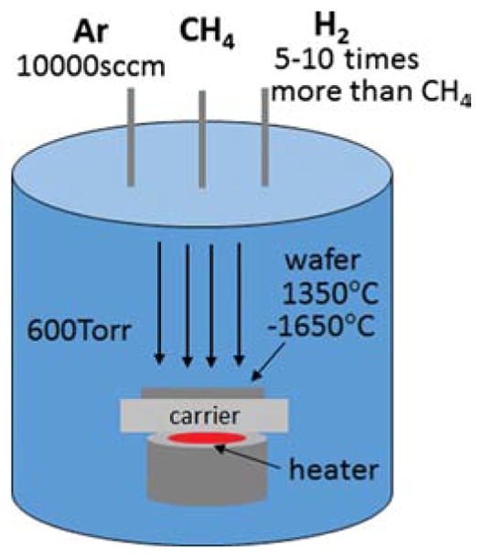
Schematic of graphene film growth by chemical vapor deposition (CVD) on a sapphire substrate in a chamber.
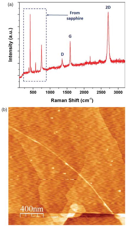
Raman signatures of graphene are detected from a metal-free CVD-grown graphene on sapphire as shown in Figure 2(a). G-band from in-plane vibration and 2D-band with the double resonance of two-phonons are observed at ~1600 cm−1 and ~2700 cm−1, respectively. D-peaks involved in defects are found at ~1350 cm−1 and the number of graphene sheets is identified as one or two monolayers (ML) by optical transmission measurements. The intensity ratio between 2D-peak and G-peak (I2D/IG = ~ 1.5) in Raman spectroscopy empirically supports the number of graphene sheets. Surface morphology of the grown graphene film is also examined using AFM as shown in Figure 2(b). It scans over the 2 × 2 μm2 film surface and the surface is verified to be smooth with the root mean square (rms) roughness of 0.31 nm. The step-like surface features are expected to be occurred from a sapphire substrate underneath the graphene sheet. There is wrinkle or fold, which can be easily detected in SiC–based epitaxial graphene.7, 33
Figure 2.
(A) Raman spectrum of graphene grown on a sapphire substrate (B) AFM image of the graphene layer.
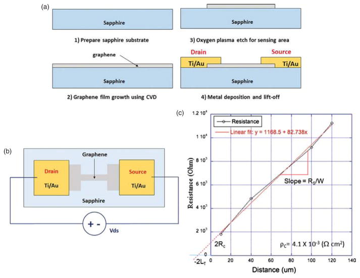
After we confirm the presence of graphene film on a sapphire substrate, electrical biosensors are fabricated using standard photolithography and etch processes. First of all, alignment marks are patterned by traditional lithography and etched using RF oxygen plasma for graphene, followed by aluminum oxide RIE protocol for the sapphire substrate. Then, the active channel regions are defined on the graphene film using optical lithography and plasma etching process. Large square graphene pads are designed at both ends of each graphene channel in order to minimize contact resistance. Drain and source metal contacts are finally patterned using lift-off process. The metal contacts are deposited onto the patterned graphene pads by an evaporator, providing sufficient attachment to the graphene pads. A simplified schematic of our fabrication process is illustrated in Figure 3(a).
Figure 3.
(A) Schematics of device fabrication process (B) schematic of sensor measurement prior to the surface functionalization (C) contact resistance analysis of the graphene devices by transmission line measurement (TLM) methods.
Connected to a precision parameter analyzer, electrical characteristics of graphene biosensors prior to its surface modification at room temperature are measured. A schematic of electrical measurements of the sensors is illustrated in Figure 3(b). Drain and source metal contacts of each sensor are connected to a DC voltage source with low voltage bias sweep from 0 to 500 mV. Each graphene sensor exhibits a linear relationship between applied DC voltage and measured output DC current, confirming each sensor is ohmic. In addition to the calculation of output resistance for each sensor, contact resistance between graphene layer and metal contacts is evaluated based on transmission line measurement (TLM).34 Figure 3(c) shows resistance plotted against TLM gap spacing, or incremental distance between two contact pads ranged from 10 to 120 μm. This TLM graph shows the parameters required for contact resistivity such as Rc, which is associated with metal-graphene interface and LT, the transfer length. Its specific contact resistivity is calculated to be ρc = 4.1 × 10⁻³ (Ω-cm2).
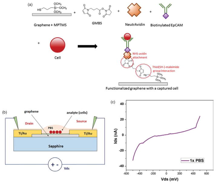
After measurements of electrical characteristics of the graphene sensors, we functionalize the surface of active graphene channel, followed by antibody immobilization. Bio-functionalization of graphene film requires several steps as described in Figure 4(a). MPTMS monolayer is first deposited directly onto the graphene nanosheet using MVD, which covalently bonds to the graphene and creates a thiol-terminated surface. GMBS solution is then applied to the MPTMS-functionalized surface to generate NHS (N -hydroxysuccinimide) terminated surface. GMBS has one end (maleimide group), which reacts strongly with thiol [–SH], and another end of NHS-terminated group. Afterwards, NeutrAvidin dissolved in PBS is introduced for the next functionalization procedure. As avidin, in the form of NeutrAvidin, is bonded to the NHS surface, it allows for easy attachment of biotinylated antibodies, suppresses nonspecific adhesion and shields the antibodies from a bare graphene/sapphire surface.35 For this particular study, biotinylated EpCAM antibody, which is known as a diagnostic marker for various epithelial cancers as well as circulating tumor cells (CTCs), is strongly immobilized to the NeutrAvidin-coated device surface.36 Prepared cancer cells suspended in PBS buffer solution are later to be loaded over the device surface using a micropipette.
Figure 4.
(A) Illustrations of the graphene surface functionalization (B) schematics of biosensor measurements after cells are adhered to the functionalized graphene surface (C) I–V characteristics of the functionalized biosensor in an open circuit configuration submerged by 1× PBS solution.
Similar to its previous electrical characterization, the surface functionalized graphene biosensor chips are loaded to a probe station and are tested with a precision parameter analyzer at room temperature. A cross-sectional illustration of electrical measurements for graphene sensors after the surface modification is described in Figure 4(b). DC voltage bias applied between drain and source contacts is maintained to be no greater than 500 mV, keeping low electrical field to prevent any damage of biological analytes. Probe tips are gently connected to the both metal contacts as they penetrate through a small drop of PBS buffer solution (~10 μl), which covers the entire functionalized sensor surface. The volume and concentration of the PBS drop are maintained to be the same as the devices are kept at high humidity to prevent evaporation. Neither of metal gate electrode nor electrolyte-gate has been implemented for this device configuration, which prominently simplifies fabrication procedure and experimental setup. Leakage current through the buffer solution via the metal electrodes is measured as the ends of both probe tips are placed inside the PBS with the same distance between drain and source contacts. Measured leakage current is considerably negligible (less than 30 nA) with the same range of DC voltage bias as shown in Figure 4(c).
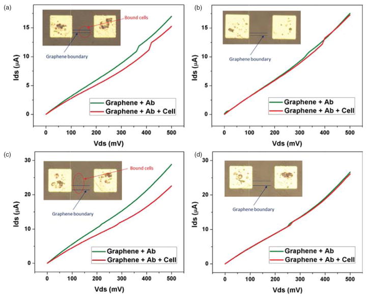
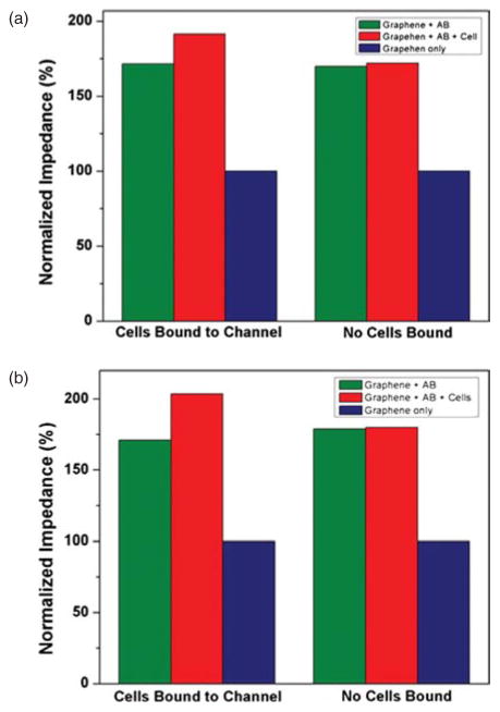
The dependence of electrical resistance of graphene biosensors due to the surface functionalization and captured cells is evaluated. Figures 5(a) and (b) show optical microscopy images of graphene biosensors array before and after their surface modification followed by the immobilization of HCT116 cells. PFA (paraformaldehyde) is applied to fix suspended cells in PBS before they are placed over the EpCAM-coated surface. After a period of incubation time, which allows antibody-cell binding interaction, followed by thorough PBS washing steps to remove excess cells, the electrical dependence of graphene sensors is re-characterized. Group of cell clusters are observed on functionalized graphene channels as shown in Figure 5(b), which caused increase in electrical resistance of the sensor. In contrast to HCT116 cells, non-EpCAM expressed cells such as macrophage cells are confirmed not to be adhered to the functionalized surface as they become mostly washed away even by a gentle PBS rinse step. I–V characteristics of the sensors, showing electrical effects from the adhered cells are plotted in Figures 6(a)–(d) for the graphene channel width of 10 and 20 μm, respectively. These graphs show non-linear response between the output DC current and input DC voltage, in contrast to their linear relationship from the bare graphene device (prior to the surface modification), where PBS acts as the electrolyte. Average resistances of graphene biosensors are tabulated in Tables I and II. For each case, the average resistance of a narrower graphene channel (10 μmm) is roughly greater by a factor of two than that of a wider channel (20 μm), which becomes consistent with the Ohm’s law. For the purpose of easier comparison between them, Figures 7(a) and (b) show the change in normalized average electrical resistances with respect to that of the bare graphene. We observe that the sensitivity of a graphene sensor with a wider channel is greater than that of a narrower channel as the percent change of normalized electrical resistance is as large as ~20% of the baseline.
Figure 5.
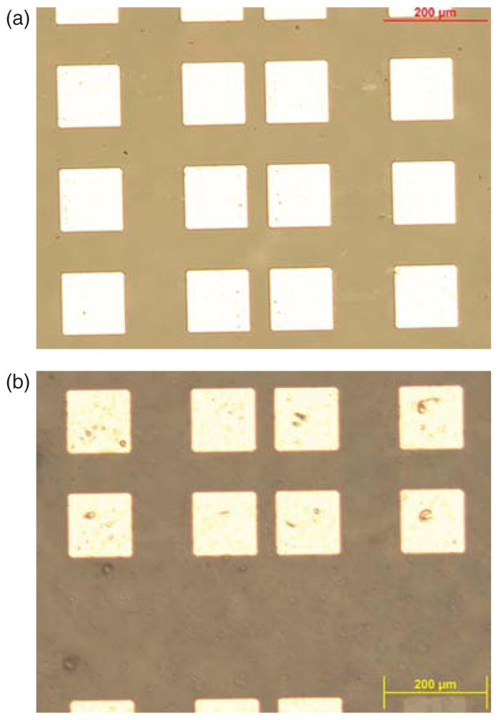
Optical microscopy images of the graphene sensors (A) before (top) (B) after (bottom) surface functionalization followed by antibody and cell immobilization.
Figure 6.
(A)–(B) I–V characteristics of the graphene biosensors before and after surface functionalization (channel width = 10 μm, with and without adhered cells, respectively). (C)–(D) I–V characteristics of the graphene biosensors before and after surface functionalization (channel width = 20 μm, with and without adhered cells, respectively).
Table I.
Average electrical resistance of the graphene biosensors (channel width = 10 μm).
| Impedance (kΩ) | After antibody immobilization | After cell adhesion |
|---|---|---|
| With cell | 28.3 | 31.6 |
| Without cell | 29.2 | 29.6 |
Table II.
Average electrical resistance of the graphene biosensors (channel width = 20 μm).
| Impedance (kΩ) | After antibody immobilization | After cell adhesion |
|---|---|---|
| With cell | 16.2 | 19.3 |
| Without cell | 18.6 | 18.7 |
Figure 7.
Analysis of normalized resistance change (A) channel width = 10 μm and (B) channel width = 20 μm.
In order to determine a graphene biosensor’s reusability, we measure electrical resistance of graphene devices after applying elution buffers to dissociate antigen-antibody interaction to detach the cells. For this purpose, we placed IgG Elution Buffer solution over the biosensor chip and washed with PBS to detach previously adhered cells. As shown in I–V characteristic plot (See Fig. 8), we observe that the resistance of a graphene device has been decreased roughly close to its initial value after elution buffer effectively washed the cells away from the graphene channels.
Figure 8.
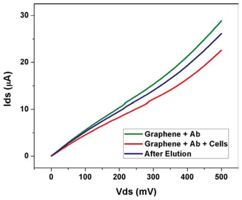
I–V measurement after elution buffer is applied to the graphene sensor (channel width = 20 um for this case).
4. CONCLUSIONS
In this work, we have described the use of surface modified electrical biosensors with CVD grown graphene nanosheet on a transparent sapphire substrate. We have demonstrated that cancer cells are detected by resistance change of the graphene device as large as ~20% of the baseline with a small number of adhered cells. The standard microfabrication and surface functionalization procedure of the graphene sensors on sapphire suggest that the biosensors are compatible with different kinds of antibodies and other types of cells and can be integrated with complementary metal-oxide-semiconductor (CMOS) based electronics. Geometrically optimized graphene sensors with electrolyte-gate configuration via electric double layer (EDL)37 may improve their sensitivity, possibly up to the level of single-cell sensing. Furthermore, we carefully anticipate that the electrical graphene sensors on a sapphire substrate will become a promising technology to monitor cellular electrical behavior and result in integration with traditional fluorescence-based bioassays in applications of real-time cancer cell detection with its anti-cancer drug treatments.
Acknowledgments
We acknowledge support for this research from the AFOSR MURI FA9550-09-1-0705 and from Cornell Center for Materials Research (CCMR: DMR-1120296). This work was performed in part at the Cornell NanoScale Facility, a member of the National Nanotechnology Infrastructure Network, which is supported by the National Science Foundation. We would like to thank Pengcheng Bu, Joyce Chen and Nikolai Rakhilin for helpful suggestions and discussions.
References and Notes
- 1.Novoselov KS, Geim AK, Morozov SV, Jiang D, Zhang Y, Dubonos SV, Grigorieva IV, Firsov AA. Science. 2004;306:666. doi: 10.1126/science.1102896. [DOI] [PubMed] [Google Scholar]
- 2.Zhang Y, Tan YW, Stormer HL, Kim P. Nature. 2005;438:201. doi: 10.1038/nature04235. [DOI] [PubMed] [Google Scholar]
- 3.Berger C, Song Z, Li T, Li X, Ogbazghi AY, Feng R, Dai Z, Marchenkov AN, Conrad EH, First PN, de Heer WA. J Phys Chem B. 2004;108:19912. [Google Scholar]
- 4.Bolotin KI, Sikes KJ, Jiang Z, Klima M, Fudenberg G, Hone J, Kim P, Stormer HL. Solid State Commun. 2008;146:351. [Google Scholar]
- 5.Das S, Kim M, Lee J, Choi W. Crit Rev Solid State Mater Sci. 2014;39:231. [Google Scholar]
- 6.Huang Y, Dong X, Shi Y, Li CM, Li LJ, Chen P. Nanoscale. 2010;2:1485. doi: 10.1039/c0nr00142b. [DOI] [PubMed] [Google Scholar]
- 7.Kim M, Hwang J, Lepak LA, Lee J, Spencer MG, Tiwari S. Nanotechnology. 2010;23:335202. doi: 10.1088/0957-4484/23/33/335202. [DOI] [PubMed] [Google Scholar]
- 8.Kim KS, Zhao Y, Jang H, Lee SY, Kim JM, Kim KS, Ahn JH, Kim P, Choi JY, Hong BH. Nature. 2009;457:706. doi: 10.1038/nature07719. [DOI] [PubMed] [Google Scholar]
- 9.Barton RA, Parpia J, Craighead HG. J Vac Sci Technol B Microelectron Nanom Struct. 2011;29:050801. [Google Scholar]
- 10.Liu Y, Dong X, Chen P. Chem Soc Rev. 2012;41:2283. doi: 10.1039/c1cs15270j. [DOI] [PubMed] [Google Scholar]
- 11.Chaubey A, Malhotra BD. Biosens Bioelectron. 2002;17:441. doi: 10.1016/s0956-5663(01)00313-x. [DOI] [PubMed] [Google Scholar]
- 12.Kuila T, Bose S, Khanra P, Mishra AK, Kim NH, Lee JH. Biosens Bioelectron. 2011;26:4637. doi: 10.1016/j.bios.2011.05.039. [DOI] [PubMed] [Google Scholar]
- 13.Jeykumari DRS, Narayanan SS. Biosens Bioelectron. 2008;23:1686. doi: 10.1016/j.bios.2008.02.001. [DOI] [PubMed] [Google Scholar]
- 14.Schedin F, Geim AK, Morozov SV, Hill EW, Blake P, Katsnelson MI, Novoselov KS. Nat Mater. 2007;6:652. doi: 10.1038/nmat1967. [DOI] [PubMed] [Google Scholar]
- 15.Ohno Y, Maehashi K, Yamashiro Y, Matsumoto K. Nano Lett. 2009;9:3318. doi: 10.1021/nl901596m. [DOI] [PubMed] [Google Scholar]
- 16.He Q, Sudibya HG, Yin Z, Wu S, Li H, Boey F, Huang W, Chen P, Zhang H. ACS Nano. 2010;4:3201. doi: 10.1021/nn100780v. [DOI] [PubMed] [Google Scholar]
- 17.Feng L, Chen Y, Ren J, Qu X. Biomaterials. 2011;32:2930. doi: 10.1016/j.biomaterials.2011.01.002. [DOI] [PubMed] [Google Scholar]
- 18.Cohen-Karni T, Qing Q, Li Q, Fang Y, Lieber CM. Nano Lett. 2010;10:1098. doi: 10.1021/nl1002608. [DOI] [PMC free article] [PubMed] [Google Scholar]
- 19.Huang Y, Dong X, Liu Y, Li LJ, Chen P. J Mater Chem. 2011;21:12358. [Google Scholar]
- 20.Su B, Tang J, Huang J, Yang H, Qiu B, Chen G, Tang D. Electroanalysis. 2010;22:2720. [Google Scholar]
- 21.Du M, Yang T, Jiao K. J Mater Chem. 2010;20:9253. [Google Scholar]
- 22.Khatayevich D, Page T, Gresswell C, Hayamizu Y, Grady W, Sarikaya M. Small. 2014;10:1505. doi: 10.1002/smll.201302188. [DOI] [PubMed] [Google Scholar]
- 23.Jang HD, Kim SK, Chang H, Roh KM, Choi JW, Huang J. Biosens Bioelectron. 2012;38:184. doi: 10.1016/j.bios.2012.05.033. [DOI] [PubMed] [Google Scholar]
- 24.Feng L, Wu L, Wang J, Ren J, Miyoshi D, Sugimoto N, Qu X. Adv Mater. 2012;24:125. doi: 10.1002/adma.201103205. [DOI] [PubMed] [Google Scholar]
- 25.Yoon HJ, Kim TH, Zhang Z, Azizi E, Pham TM, Paoletti C, Lin J, Ramnath N, Wicha MS, Hayes DF, Simeone DM, Nagrath S. Nat Nanotechnol. 2013;8:735. doi: 10.1038/nnano.2013.194. [DOI] [PMC free article] [PubMed] [Google Scholar]
- 26.Alava T, Mann JA, Théodore C, Benitez JJ, Dichtel WR, Parpia JM, Craighead HG. Anal Chem. 2013;85:2754. doi: 10.1021/ac303268z. [DOI] [PubMed] [Google Scholar]
- 27.Huang X, Yin Z, Wu S, Qi X, He Q, Zhang Q, Yan Q, Boey F, Zhang H. Small. 2011;7:1876. doi: 10.1002/smll.201002009. [DOI] [PubMed] [Google Scholar]
- 28.Ehret R, Baumann W, Brischwein M, Schwinde A, Stegbauer K, Wolf B. Biosens Bioelectron. 1997;12:29. doi: 10.1016/0956-5663(96)89087-7. [DOI] [PubMed] [Google Scholar]
- 29.Prasad S, Quijano J. Biosens Bioelectron. 2006;21:1219. doi: 10.1016/j.bios.2005.05.005. [DOI] [PubMed] [Google Scholar]
- 30.Chen SW, Yang JM, Yang JH, Yang SJ, Wang JS. Biosens Bioelectron. 2012;33:196. doi: 10.1016/j.bios.2011.12.052. [DOI] [PubMed] [Google Scholar]
- 31.Shinde AV, Motiani RK, Zhang X, Abdullaev IF, Adam AP, González-Cobos JC, Zhang W, Matrougui K, Vincent PA, Trebak M. Sci Signal. 2013;6:ra18. doi: 10.1126/scisignal.2003425. [DOI] [PMC free article] [PubMed] [Google Scholar]
- 32.Kim M, Hwang J, Cha HY, Spencer MG, Lee JW. J Nanosci Nanotechnol. 2014;14:2979. doi: 10.1166/jnn.2014.8583. [DOI] [PubMed] [Google Scholar]
- 33.Kim M, Hwang J, Shields VB, Tiwari S, Spencer MG, Lee JW. Nanoscale Res Lett. 2012;7:186. doi: 10.1186/1556-276X-7-186. [DOI] [PMC free article] [PubMed] [Google Scholar]
- 34.Berger HH. Solid State Electron. 1972;15:145. [Google Scholar]
- 35.Gleghorn JP, Pratt ED, Denning D, Liu H, Bander NH, Tagawa ST, Nanus DM, Giannakakou PA, Kirby BJ. Lab Chip. 2010;10:27. doi: 10.1039/b917959c. [DOI] [PMC free article] [PubMed] [Google Scholar]
- 36.Nagrath S, Sequist LV, Maheswaran S, Bell DW, Irimia D, Ulkus L, Smith MR, Kwak EL, Digumarthy S, Muzikansky A, Ryan P, Balis UJ, Tompkins RG, Haber DA, Toner M. Nature. 2007;450:1235. doi: 10.1038/nature06385. [DOI] [PMC free article] [PubMed] [Google Scholar]
- 37.He RX, Lin P, Liu ZK, Zhu HW, Zhao XZ, Chan HLW, Yan F. Nano Lett. 2012;12:1404. doi: 10.1021/nl2040805. [DOI] [PubMed] [Google Scholar]


