Abstract
Electronic biosensing is a leading technology for determining concentrations of biomolecules. In some cases, the presence of an analyte molecule induces a measured change in current flow, while in other cases, a new potential difference is established. In the particular case of a field effect biosensor, the potential difference is monitored as a change in conductance elsewhere in the device, such as across a film of an underlying semiconductor. Often, the mechanisms that lead to these responses are not specifically determined. Because improved understanding of these mechanisms will lead to improved performance, it is important to highlight those studies where various mechanistic possibilities are investigated. This review explores a range of possible mechanistic contributions to field-effect biosensor signals. First, we define the field-effect biosensor and the chemical interactions that lead to the field effect, followed by a section on theoretical and mechanistic background. We then discuss materials used in field-effect biosensors and approaches to improving signals from field-effect biosensors. We specifically cover the biomolecule interactions that produce local electric fields, structures and processes at interfaces between bioanalyte solutions and electronic materials, semiconductors used in biochemical sensors, dielectric layers used in top-gated sensors, and mechanisms for converting the surface voltage change to higher signal/noise outputs in circuits.
1. Introduction
1.1. General background
Electronic biosensors remain attractive as means of determining concentrations of biomolecules in biological fluids. They offer significant advantages in manufacturability, ease of use, and throughput compared to alternatives such as ELISA, microcantilever, and spectroscopic approaches. To quote one prior review on the subject: “Electrical analytical methods commonly have an innate high sensitivity and simplicity that can be effectively married to miniaturized hardware. As such, they constitute, arguably, the most practical, quantifiable and scalable of all low cost diagnostic assessments of protein presence.”1 Electronic biosensors can be amperometric, voltammetric, potentiometric, conductometric, impedance, or field effect, and may be based on oxidation/ reduction reactions. Thus, in some cases, the presence of an analyte molecule induces a measured change in current flow, while in other cases, a new potential difference is established. In the particular case of a field effect biosensor, the potential difference is monitored as a change in conductance elsewhere in the device, such as across a film of an underlying semiconductor.
There are numerous mechanisms by which chemical reorganization and binding in response to the presence of a bioanalyte can result in changes in measured electronic properties. Often, the details of these mechanisms are not considered in detail, as more empirical means are used to optimize device responses. This leaves open the possibility that the responses are not as strong or selective as they could be, or even that the responses arise from effects not considered in the original device design. Thus, it is important to highlight those studies where various mechanistic possibilities are explored. This review is intended as a presentation of a range of possible mechanistic contributions to field-effect biosensor signals. First, we define the field-effect biosensor and the chemical interactions that lead to the field effect. This is followed by a section on theoretical and mechanistic background. We then discuss materials used in field-effect biosensors and approaches to improving signals from field-effect biosensors.
1.2. Field effect devices
While chemical changes at an electrode surface can affect voltages and currents in the circuit with which the changing chemical components are in series, it is often desirable to transduce these changes into an external circuit. Field-effect transistors (FETs) are an important class of “label-free” detection methods which do not require signal amplification functionality to be chemically attached to analytes. Such label-free methods have recently been reviewed.2,3 The FET geometry has been increasingly considered for biosensing in the last two decades,4–12 with the ability to detect proteins and nucleic acids in real time using antibodies and nucleic acid conjugates, respectively, as receptors. Analytes can be identified either by a specific interaction between analyte molecules and a receptor on a semiconductor surface or near the surface of an adjacent dielectric.
A number of properties are required for a semiconductor before its application to biochemical sensor devices: high mobility, excellent stability, long operation lifetime, low-cost processing, and environmental friendliness to name a few. To date, there are many kind of semiconductors employed as active layers for biosensor. These include inorganic semiconductors such as Si, MoS2 and SnO2, organic and polymer semiconductors (OSCs) such as poly(3-hexylthiophene) (P3HT), pentacene, naphthalenetetracarboxylic diimides (NTCDIs) and sexithiophene (a-6T), and some low dimensional organic semiconductors, for example, carbon nanotubes and graphene. Inorganic semiconductors (except for hydrogenated amorphous silicon, α-Si:H) generally show higher mobility, greater chemical stability and longer operational lifetime than the organics; however, the organics offer particular advantages as well, such as processing latitude and precise chemical definition.
Field effect biosensors include those based on organic and nanostructured FETs. Organic FETs (OFETs)13–20 are being developed for active matrix backplanes,21 radiofrequency identification (RFID) tags,22 and chemical,9,23 mechanical,24,25 and biological sensing.8,9,26 OFET operation has been thoroughly reviewed.27–35 For OFETs used as biosensors so far, sensitivity has been lower than what is considered medically necessary (ng to μg mL−1). Sensitivities down to pg mL−1 were instead achieved from large surface/volume nanostructured/low dimensional condensed materials, e.g. Si nanowires,36–38 SnO2 nanobelts,39 single-crystalline Si,40 carbon nanotubes,41–45 and graphene.46
1.3. Biomolecular recognition in FET devices
The most frequently used biochemical interactions harnessed for field-effect biosensors are antibody–antigen complexing,47,48 complementary single-stranded DNA,49–51 and enzyme–substrate interactions.52–55 While the incorporation of each of these methods into field-effect transistor devices provides the potential for a highly specific interaction and sensing event, there are also numerous difficulties to be overcome for the purposes of commercialization.56 Among those drawbacks previously discussed in the literature include the difficulty mass producing device,57 the necessity to encapsulate parts of the devices or keep it in an aqueous buffer,58 poor reproducibility,59 and inconsistent attachment of biological receptors.60 Above all, the interactions must result in electronic perturbations at a device interface.
The antibody–antigen interaction is one of the most specific in biology, and has been widely explored as an option for functionalizing field-effect transistor biosensors. The binding of an antigen of interest to an antibody provides an electrical shift in the sensing layer, typically proportional to the amount of antigen present in solution.55 However, a frequent issue with this method is the physical size of the antibody being on the order of the Debye length of the solution.61 In an attempt to avoid screening the electrostatic effect of a binding event, there has been a great deal of success using smaller antibody fragments such as single chain variable fragments (scFv).62,63 By only using the binding portion of the antibody, the binding event is physically closer to the sensing substrate, and concentrations down to pg ml−1 have been successfully sensed. Jang et al. additionally circumvented the issue of the Debye length through an electrically (rather than optically) active ELISA approach, which was also able to achieve pg ml −1 sensitivity.61
Jun reported the use of aptamers bound to carboxylated polypyrrole-coated metal oxide-decorated carbon fibers as a transducer medium. Aptamers have been used instead of antibodies owing to the stability and high selectivity of the aptamers as well as the ability to make them by direct chemical synthesis methods.64 The instability of antibodies has been a weak link in receptor-based biosensor development; perhaps aptamers can help address this issue more broadly.
Single-stranded DNA can be immobilized on the surface of FETs and maintain its ability to hybridize with complementary strands.65,66 The two strands of DNA contain complementary elements (adenine–thymine and cytosine–guanine). The target single-stranded DNA (ssDNA) is identified by a probe ssDNA immobilized on the sensitive surface. The probe ssDNA will form a double-stranded DNA (dsDNA) helix structure with the complementary target ssDNA with excellent affinity, significantly greater than that of noncomplementary nucleic acids. The analyte DNA has a strongly negative charge and is able to shift the threshold voltage of the FET device significantly with relatively few hybridization events. As with antibody–antigen complexing, the binding event can be screened due to its distance from the sensing surface.
Distinct from the above events are enzyme–substrate interactions. Rather than relying on a single binding event, the enzyme–substrate interactions used in FET biosensors typically produce electroactive species that result in a local pH shift near the sensing surface.67,68 Very generally, enzymes are immobilized on or near active electrodes and are immersed in solution that may have some electrically active helper analyte in it, where a specific substrate binding event will produce an output.69,70 Common enzyme FETs include those for penicillin,54,71 urea,60,72 and sugars.73 Among the most important of these is the glucose sensor, as it was recently estimated to make up 85% of the biosensing market.74 Great advances have been made to increase the sensitivity and speed of glucose FET biosensors in recent years.73,75,76 Park et al. fabricated a glucose oxidase FET-type biosensor with a detection limit of 1 nM and speed of under 1 second, which was shown to be both reproducible and stable up to one month.77 In the use of five-times diluted real samples, it was shown to give similar results to commercially available glucose sensors and gave readings in the mM range. You et al. also tackled the stability issue of biological FETs by incorporating silk fibroin encapsulation onto a glucose sensor.58 This was an effective way to maintain stability at room temperature for over ten months, and showed good sensitivity in the 0.1–10 mM range of interest.
The sensor response using enzymes as a functionalization layer can be influenced by many factors, such as the buffer capacity, ionic strength, pH of the solution, enzyme immobilization and the deposition methods. To better control these factors, several solutions have been proposed, for example, the addition of polymeric membranes such as Nafion, poly-(4-vinylpyridine-co-styrene) or poly(acrylamide) gel (PAAG) which can control the diffusion of substrate and product.78–81 Moreover, when adding hydroxyl ions to the enzyme membrane is found to improve the sensitivity, this can be accomplished by applying a negative polarization on the integrated platinum electrode.82
While ever higher sensitivities of biological FETs (bioFETs) have been developed in laboratories since their inception, there has been relatively little overall success in commercialization of these sensors.56 To be commercially successful, biosensors must meet minimal general criteria: sensitivity of medical interest, high specificity to the analyte of interest, shelf stability, and high speed and convenience for easy use. Quite frequently, bioFETs sacrifice one or more of these criteria in an attempt to improve another. One of the most frequent checks of specificity in the cited literature is bovine serum albumin (BSA): BSA is exposed to the sensor, and if there is minimal measured response, the sensor is assumed to be highly specific. While this is an effective first test, it would be of even more interest to expose the bioFET to chemically similar species (for example, in the case of glucose the bioFET could be exposed to other fructose, maltose, etc., to ensure complete specificity). The sensitivity of bioFETs is also rarely tested in the presence of any solution more complex than PBS.61 This makes it unclear of the sensitivity of the bioFET in the presence of real human samples such as blood or urine, which include many additional species that could inadvertently interact with the sensor. Some groups attempt to alleviate this by dilution or desalting the real sample.83 While this may be effective in some cases, it poses the risk of lowering the concentration of the analyte of interest as well as adding an additional, time-consuming step. The stability of bioFETs has also been measured, with mixed results.60 Many groups have seen a sharp decrease in the number density of attached enzymes in the days following attachment, presumably due to non-specifically aggregated enzymes detaching from near the substrate. After this initial decrease, the attached enzymes typically have relatively good stability on the order of months.
Additional difficulties regarding commercialization come from the manufacture of bioFET devices. While encapsulation methods prove impressive on the small scale, it is not clear how easily this technology would be reproducible at a large scale. The necessity to keep parts of the bioFET under aqueous solution provides an additional difficulty for storage. Since enzyme and antibody attachment as reported is a largely manual process, there are reports of large differences in signal between various batches produced in the laboratory.59 It is necessary to further standardize these methods of attachment for large-scale manufacturing.
1.4. Enzymatic reactions in biosensors
The most prominent type of enzyme used in field-effect biosensors is the oxidoreductase class. As the name implies, oxidoreductases are responsible for transferring electrons from a reductant to an oxidant. These enzymes quite frequently require additional molecules (called cofactors and coenzymes, whose exact definitions vary by source) to function properly, such as NADP/NAD+. The method of electron transfer can occur in any number of mechanisms including transfer of a hydride and proton, transfer of two electrons and two protons, transfer of a hydrogen, electron and proton, and many other combinations.84 Glucose oxidase is a common oxido-reductase that produces oxygen and hydrogen peroxide as a result of its use of flavin adenine dinucleotide (FAD) as an electron-accepting cofactor. FAD is used by other enzymes in similar fashion, including Acyl CoA dehydrogenases, another important enzyme involved in eukaryotic metabolism. Alcohol dehydrogenases (ADH) reduce a cofactor nicotinamide adenine dinucleotide (NAD+) as part of their mechanism of action. The result of this enzyme is often an aldehyde product in place of the alcohol and a proton released into solution. These protons are responsible for changing the local pH of the surrounding solution.
Electrochemical detection of glucose is an important goal for carbon nanotube sensors. The mechanism is based on glucose oxidation catalyzed by the redox enzyme glucose oxidase (GOx) to D-glucono-1,5-lactone.85 The redox enzymes go through a catalytic reaction cycle, where groups in the enzyme temporarily change their charge state, and conformational changes occur in the enzyme, which can be detected by using nanotube FET (NTFET) devices. Therefore, by immobilizing GOx on carbon nanotubes, glucose detection can be realized in real time through measuring conductance of the NTFET while immersed in the reaction medium. No obvious conductance change was observed as a result of water addition, but when 0.1 M glucose in DI water was added to liquid, the conductance of this SWNT increased by about 10%, regardless of its original value. Glucose did not change the conductance of bare SWNTs. The results clearly indicate that the GOx activity is responsible for the measured increase in conductance upon glucose addition (Fig. 1).
Fig. 1.
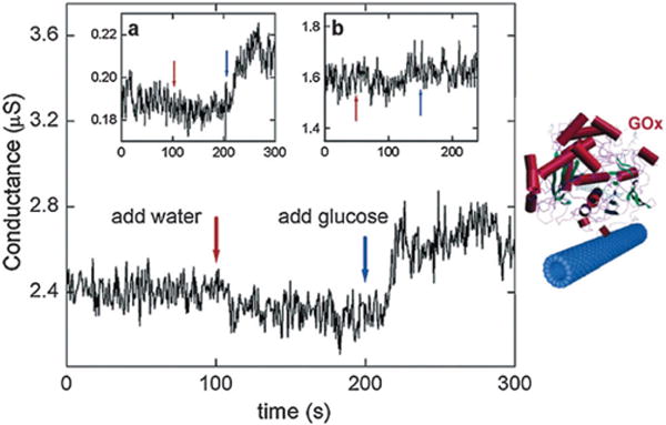
Left: real time electronic response of an NTFET sensor to glucose, the substrate of GOx. The conductance of a semiconducting SWNT with immobilized GOx is measured as a function of time in 5 lL milli-Q water. The conductance of the GOx-coated SWNT is observed to increase upon addition of glucose to the liquid. Insets: (a) the same measurement on a second device, where the conductance was a factor of 10 lower; (b) the same measurement on a semiconducting SWNT without GOx. No conductance increase is observed in this case. Copyright Nano Letters, American Chemical Society.85
Other enzymatic reactions produce voltage changes that so far have been detected potentiometrically, but if coupled to an FET gating mechanism, could also be amplified using FET-based circuitry. For example, the transferases are a group of enzymes involved in transferring specific functional groups from an acceptor to a donor molecule. They are extremely important in biological systems, and would be beneficial to sense more accurately since deficiencies in various transferases are linked to Huntington’s disease86 and schizophrenia,87 among many others. One widely studied reaction, the binding of glutathione (GSH) to glutathione transferase involves the release of a proton during each enzymatic event. While pH measurements are complicated by the fact that the speed of enzymatic reactions varies as a function of pH, by adding substrate to a solution of glutathione transferase and titrating backward to return to the original pH value, it is possible to calculate the total amount of proton released from the reaction.88 Another relatively simple sensing mechanism of a transferase is measuring the level of transketolase activity. This method relies of the decarboxylation of lithium hydroxypyruvate (HPA) with an aldehyde acceptor. The subsequent release of carbon dioxide results in the pH increase that is easily seen by the phenol red indicator, and could also be measured by a potentiometric sensor.89
Lyases are the group of enzymes that break a bond in their substrate by a method that is not hydrolysis, and differentiate themselves from other enzymes further since they require only a single molecule for the forward reaction but two for the reverse reaction. Conversely, ligases are the group of enzymes that catalyze the binding of two larger molecules together, frequently by releasing smaller functional groups in the process.90 These enzymes can be part of a cascade chemistry of multiple enzymes that results in an electroactive substance capable of producing an electrical potential.91 One example of this is the combination of citrate lyase combined with oxaloacetatecarboxilase and pyruvate oxidase.92 The final reaction of this system uses oxygen, phosphate, and pyruvate to form acetylphosphate, carbon dioxide, and hydrogen peroxide. The oxygen-sensitive electrodes of the potentiometric sensor in this system measure the decrease in oxygen over time. Another example of an enzyme that could be used in a cascade is the isomerase class, responsible for rearranging functional groups on a single molecule. While the shape of the molecule may change, the chemical formula (and therefore the overall charge) will stay the same with no extra electroactive products formed. It is possible for isomerases to be useful in electrochemical sensors in conjunction with other types of enzymes downstream in a chain reaction, if the following enzyme reactions produce an electroactive species. An example of this is the coupling of glucose isomerase and glucose oxidase to aid in conversion of sucrose to glucose.93
A schematic summary of the positioning and charging effects of these enzymes is shown in Scheme 1.
Scheme 1.
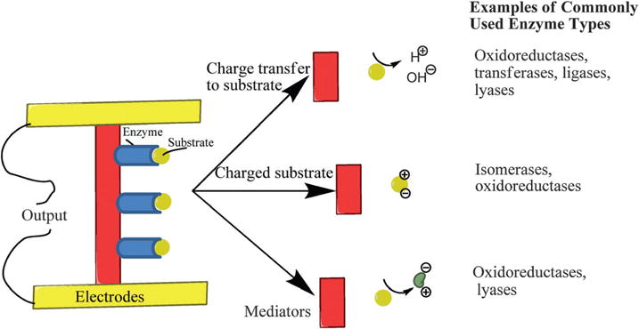
Common examples of different types of enzymes used in potentiometric sensing.
2. Transduction mechanisms at the analyte medium-device interface
2.1. The electrical double layer
Charge redistributions occurring when device surfaces are in contact with electrolyte solutions can lead to changes in surface potential. The theory of the electrical double layer gives a good illustration of the potential-change phenomenon, as illustrated in Fig. 2,94 and is influenced by major factors such as the ionic strength and pH of the analyte solution.
Fig. 2.
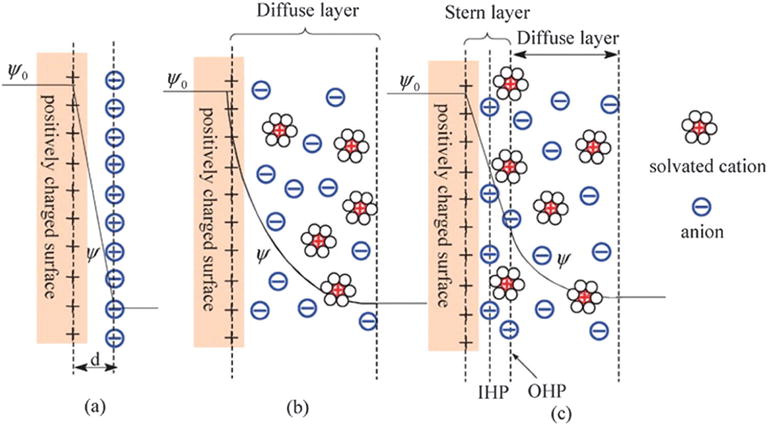
Schematic representations of electrical double layer structures describing (a) the Helmholtz model, (b) the Gouy–Chapman model and (c) the Gouy–Chapman–Stern model. Copyright Chemical Society Reviews, Royal Society of Chemistry.94
The model of the electrical double layer, as illustrated in Fig. 2a, was initially described by Von Helmholtz95 specifying that two layers with opposite charges are formed in the electrolyte and electrode, and they are separated by a certain distance. This model was modified by Gouy equations:
| (1) |
| (2) |
where C0 and z are respectively the concentration of ions in the bulk solution and the valence of ions, ε0 is the permittivity of free space, εr is the dielectric constant of the solution, T is the temperature, k Boltzmann constant and Ψ and Ψ 0 are respectively the potential in each point in the solution and the potential at the interface solid/electrolyte.
A more realistic description of the electrostatic double layer was proposed in the Stern theory combining the Helmholtz model and the Gouy–Chapman model96 to describe the ion distribution in the Stern layer and the diffuse layer. The Stern layer97 is formed and subdivided into two regions of inner and outer Helmholtz planes referred to respectively as IHP and OHP, as shown in Fig. 2c. These two planes explain the existence of a capacitance Cd of electrical double layer close to the solid/electrolyte interface, consisting of two capacitances in series, the Stern capacitance CS and the diffuse layer capacitance CD. The thickness of the diffuse layer is assessed by Debye length λD, giving the distance from the OHP into the solution up to the point where the electrostatic effect of the surface is felt by the ions. The detection limit of biosensors is highly dependent on the Debye screening length between the sensitive material surface and the electrolyte solution.
2.2. Influence of charge screening on biomolecule detection
During the last several decades, biosensor devices have been widely studied, focusing on surface binding interactions involving small molecules, protein–protein interactions, antibody–antigen binding, DNA and RNA hybridization, and receptor–ligand interactions.98–100 The interface between the sensor surface and electrolytic solution strongly influences the sensor response, and needs to be understood mainly for devices with small dimensions or when the concentration to be detected becomes very low. The basic mechanisms for these different interactions are hybridization, surface polarization effects or dipole moment change, adsorption and affinity binding of different biomolecules as illustrated in Fig. 3.
Fig. 3.
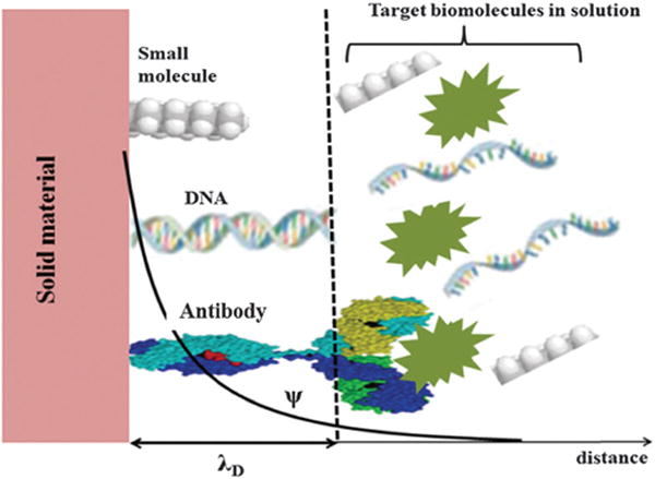
Schematic representation of different bindings and biomolecule size inside and outside the electrical double layer with different targets. Only the diffuse layer of the electrical double layer is represented. The biomolecule detection must occur inside the electrical double layer.
It is known that several types of biomolecules have electrostatic charges under normal physiological media. For example, DNA molecules have a negatively charged phosphate backbone and can be considered as a circular cylinder, about 1.5–2 nm in diameter with charges distributed on the cylindrical surface.101 Most nucleic acids such as DNA or RNA have their respective detection techniques based on some sort of hybridization process,102–105 which can effectively influence the distribution of the charge density in the double layer. The detection of DNA is difficult due to the charge screening effect as observed in many biomolecules detection system such as that of proteins (to be described later). However, the DNA molecules have a unique structure in that the length of a nucleotide, or base, is estimated to be around 0.34 nm, but the redistribution resulting from the hybridization can be detected in physiological solutions.106,107
The charge on proteins depends on the pH of the solution in which they are dispersed, which can greatly affect the sensor device. The isoelectric point (pI), defined by the pH at which the charge of the protein is equal to zero, gives an idea of the protein charge according to the value of pH in the solution. Below this pI, the protein is positively charged. It is important to note that the pH at the interface is different from that in bulk as defined by the Boltzmann equation; it is not trivial to characterize the charge redistribution induced by protein binding. Stern et al.108 have shown that counterions present in buffer solutions are responsible for Debye screening and have an influence on the response to protein sensor. The surface charge of biomolecules in a buffer solution is surrounded by opposite charges in the solution and on a certain length scale, the number of net negative (positive) charges approaches the number of positive (negative) charges on the molecules as described by Park et al.;109 the electrostatic potential resulting from the variation in the surface charge density of the analyte molecules declines towards zero due to this screening effect. For an electrolyte buffer solution, this length can be expressed as following:
| (3) |
Where λD is the Debye length, ε0 and εr are defined earlier, NA is Avogadro’s number and I the ionic strength given by this expression:
| (4) |
Ci is the concentration of ion i and zi the charge of the ith ionic species. For a symmetrical electrolyte with zi = +1 and −zi = −1 the ionic strength can be replaced by the ion concentration. This Debye length determining the total thickness of the electrical double layer, it is inversely proportional to the square root of the ionic strength, we can also expect that a low electrolyte concentration induced a high Debye length110 suitable for relevant detection as summarized in Table 1.111
Table 1.
Debye length for different KCl concentrations, taken from ref. 111. Copyright Reviews of Modern Physics, American Physical Society111
| KCl concentration (M) | Debye length λD (nm) |
|---|---|
| 1 | 0.3 |
| 10−1 | 1.0 |
| 10−2 | 3.1 |
| 10−3 | 9.6 |
| 10−4 | 30.5 |
| 10−5 | 96.3 |
The work developed by Stern et al.108 has also shown the influence of buffer ionic strength on the sensor response based on nanowire transistor device. Using the biotin–streptavidin ligand–receptor system, where the biotin is the recognition element and streptavidin the targeted element, the authors showed a current increase when λD is around 7.3 nm corresponding to 0.01 × PBS. This behavior is the consequence of the fact that the majority of the protein’s charge is unscreened at the nanowire transistor. The use of the ionic strength of a 0.1 × PBS buffer, with a λD value around 2.3 nm, showed a partial screening effect of the charge of streptavidin, and in the solution with 1× PBS (0.7 nm of λD) the sensor response is strongly screened. They also showed for the binding of charged biomolecules that can participate to the response of the sensor device, the Debye length must be carefully matched a to the size (as also observed in Fig. 4) and the binding distance of the target species. The dilution of the buffer in order to obtain a larger Debye length is not effective when protein function and/or binding are affected at lower ionic strengths.
Fig. 4.
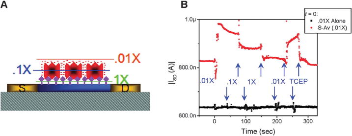
Effect of buffer dilution on sensor response from Stern et al. ref. 108, (A) represents the schematic structure of FET device using nanowire with different Debye length. The blue bar represents the active region of the device, the yellow regions the leads ((S) source, (D) drain), the gray hashed region the underlying oxide, the purple diamonds are biotin, and the red objects are streptavidin, (B) is the sensor response. Copyright Nano Letters, American Chemical Society.108
The binding of biomolecules such as DNA, proteins or small molecules must occur within the electrical double layer as shown in Fig. 4, in order to maximize sensitivity. The much shorter λD compromises the sensitivity by leaving a major charged portion of the biomolecules outside the double layer leading to the charge screening effect. The size of some biomolecules could be much larger than the Debye length, and in this case the transduction remains very difficult because the sensor response will be screened. Depending on the size of the biomolecules, the composition of the solution to be used is very important. Lloret et al.112 investigated several important consequences of the dilution of the buffer for the measured signal due to effects on protein function, protein charge, buffer capacity, ionic strength and Debye length of the solution. They concluded that the change of the charges is only detectable if it occurs at an appropriate distance above the surface compared to the Debye length, and it is importance to select an appropriate Debye length based on the size of the biomolecules involved in the detection system. However, in a counterexample, Palazzo et al. claimed detection at 30 times the Debye length distance using an electrolyte-gated OFET. According to the study, the reported bio EGOFET has a capacitive response, which was independent of the binding event distance. No effect of the Debye length was seen in the experiments, though Debye screening was said to affect the electrostatic kind of interaction. Thus capacitive sensing could lead to detection in higher ionic strength electrolytes with greater accuracy.113
Lower diameters of nanomaterials have been associated with the higher sensitivity owing to the increased area to volume ratio. Although a recent simulation by Shoorideh demonstrated that concave surfaces face less Debye screening then convex surfaces, by that argument smaller wires would have more convex surfaces leading to stronger Debye screening, thus discrediting the diameter size argument relating to the sensitivity. According to the report, nanowires on insulating surfaces have concave corners at the interfaces, decreasing the screening and increasing the sensitivity to the charged biomolecules species in return.114
Apart from the classical double-layer description of the biomolecule-related chemical interaction, several authors showed the influence of the Donnan effect115,116 using the ISFET platform. When biomolecules are attached to the sensor surface, a thick ion-permeable layer is formed between the surface and the electrolyte. The potential profile comes from the fixed charges in the membrane layer. The biomolecule membrane formed from protein and solution can be seen as two phases: a membrane phase (phase m) and solution phase (phase s). Since smaller ions can diffuse easily between phases m and s, a difference of ion concentrations is established between the two phases as a result of fixed charges in the protein membrane, leading to a potential drop. The potential difference between phases m and s is the Donnan potential expressed as:
| (5) |
where CS is the salt concentration in the electrolyte solution and CX the effective fixed charge density in the protein membrane. The author also showed that this Donnan effect affects both the Donnan potential and the pH, and φD increases by decreasing CS or by increasing CX.
De Vico et al. studied the charge distribution within the protein and the Debye length-dependent sensor response. Their studies yield tools to understand and predict the electrostatic effect of protein interactions with the surface, but they cannot provide the knowledge of protein orientation at the surface or conformal change on binding.117,118 The effects of adsorbed biomolecules on the sensor surface are interrelated in a complex way to the interfacial charge, the ionic strength of the solution, the pH of the solution, the effective distance of the biomolecule from the surface, and the chemically induced alterations.116
2.3. Overcoming charge screening effects
It is a major challenge to operate biomolecule sensor under physiological conditions. It is well known that the sensitivity is strongly impeded by charge screening effects in real biological environments such as blood. This behavior is due to the concentration of electrolyte being generally higher than 100 mM. The associated Debye length is very short and less than a nanometer, reducing the electric field created by charged biomolecules at the surface of FET, making the detection very difficult. In addition to the media used to reduce charge screening (e.g., low ionic strength), several strategies have been suggested to overcome the charge screening limitation of FET sensors.
Gao et al.119 incorporate a porous and biomolecule permeable polymer layer on the silicon nanowire field-effect transistors (SiNW FET) sensor. The role of this polymer layer is to increase the effective screening length in the region immediately adjacent to the device surface and thereby enable detection of biomolecules in high ionic strength solutions in real-time. Using an additional polyethylene glycol (PEG) modification, the authors show that prostate specific antigen (PSA) can be readily detected in solutions with phosphate buffer (PB) concentrations as high as 150 mM, while similar devices without PEG modification only exhibit detectable signals for concentrations ≤ 10 mM. Concentration-dependent measurements exhibited real-time detection of PSA with a sensitivity of at least 10 nM in 100 mM PB with linear response up to the highest (1000 nM) PSA concentrations tested. Fig. 5 illustrates the surface modification and the sensor response in this work.
Fig. 5.
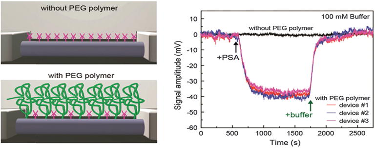
Polymer surface modification to increase the effective Debye length for FET biosensing. (left) Schematic illustration of a NW FET device (top) without and (bottom) with a porous and biomolecule permeable polymer (green) surface modification. (right) Sensor response with and without PEG polymer. Copyright Nano Letters, American Chemical Society.119
Kulkarni et al.120 reported a high-frequency measurement technique that can be applied to biological receptors. Knowing that the sensitivity of the devices suffers from the ionic screening due to mobile ions present in the solution, they demonstrate a new high-frequency sensing platform to overcome the ionic screening effect by operating a single-walled carbon nanotube FET sensor at megahertz frequency range. Electrical detection of monolayer streptavidin binding to biotin in 100 mM buffer solution was achieved at a frequency beyond 1 MHz as observed in Fig. 6. The specificity of their work is distinguished by the fact that they detect biomolecular dipoles at high frequency rather than the associated charges.
Fig. 6.

Ming current measurement setup with AM modulated input at source electrode. Sensor response with varying background ionic strength at f = 500 kHz (black-filled square) and f = 10 MHz (red-filled circle). The solid line is the logarithmic fit to the experimental data at f = 500 kHz. Copyright Nano Letters, American Chemical Society.120
Other studies121,122 used the combination of an enzyme-linked immunosorbent assay (ELISA) with an ion-sensitive field-effect transistor (ISFET). Stern and co-workers121 presented a novel configuration producing a local enzyme-mediated pH change proportional to bound ligand concentration. By monitoring the urease-induced pH increase, they calculated the quantity of bound protein in a configuration that eliminates concerns over Debye screening in high-salt buffers. They used In2O3 nanowire FETs configured as pH sensors and assessed the detection of interleukin-2 (IL-2) in physiologically buffered solution at concentrations as low as 1.6 pg mL−1. Jang et al.122 also proposed to overcome the Debye screening effect. The authors made a novel electrical immunosensor by combining the ELISA with alkaline phosphatase (ALP) labels and an ISFET platform (Fig. 7). They verified the system through the detection of the human interleukin-5 IL-5. Ag precipitation induced by the alkaline phosphatase. The result was a dramatic enhancement of the detection signal and the circumvention of the Debye length issue. Their sensor platform surpassed the sensing capability of conventional ELISA that is considered to have a limit of detection on the order of 1 ng mL−1.
Fig. 7.

(a) Schematic and (b) real images of the electrical immunosensor for point-of-care devices. ELISA employing ALP labels is combined with ISFET platform in order to impose electrical signal with high sensitivity, (c) Electrical signal variation of 100 ng mL−1 IL-5 enhanced by APL label and Debye screening length in different PBS concentrations. Copyright Biosensor and Bioelectronics, Elsevier.122
Several other groups reported an approach using short receptors123,124 to reduce the distance between the transistor surface and biomolecule analyte being detected. Elnathan and co-workers124 have demonstrated that fragmentation and size reduction of the bioreceptor antibody molecules can be effectively implemented in overcoming the detrimental screening effects associated with the sensing of biomolecules under physiological high ionic strength conditions. This simple and effective approach allows for the sensitive and direct detection of protein species under physiological environment without the strict desalting requirements associated with the use of large whole immunoglobulin (IgG) capturing species down to the pM concentration range.
2.4. Site-binding model
Theoretically, the site-binding model developed by Yates et al.125 was applied to oxide. In most of the cases, the metal oxide surfaces have a very large number of unfulfilled bonds. When such surfaces are immersed in electrolytic solution, they acquire a surface charge controlling their interfacial behavior. This charge comes from the dissociation of surface functional groups associated with the non-bulk bonding. (It is worth noting that a similar process could be extended under certain conditions to the ionization of carbon surfaces or sulfides as well.) For example, when a metal oxide surface is exposed to water, adsorption of water molecules produces a hydroxylated surface, where the hydroxyl groups at the surface can be protonated and/or deprotonated leading to a change of the oxide surface potential. It is worth noting that the protonation/de-protonation reactions at this solid material involve protons and surface hydroxyl groups. In this case, the concept of Debye screening is irrelevant since the species and the reactive surface elements have sizes on the order of Angstrom, much smaller than typical Debye length in physiologically similar buffer solutions.
The surface potential Ψ0 is distributed at the interface according to the electrical double layer theory, approximated by the Gouy–Chapman–Stern model. Taking into account the electrochemical phenomenon occurring at the interface, the relationship between the surface potential and pH are demonstrated as following:
| (6) |
and the sensitivity is defined by:
| (7) |
Where S is the pH sensitivity, pHpzc is the pH of the point of zero charge, and β is a parameter depending on the material properties such as the constants of dissociation and the number of reactive available sites126,127 at the surface of electronic material as well as the electrolyte composition128,129 affecting the double layer capacitance Cd.
3. Semiconductors
3.1. Inorganic semiconductors
The stability of silicon is especially advantageous for biosensing performed in aqueous solutions. Silicon semiconductors can be introduced as active layers in various forms, such as polycrystalline silicon film, α-Si:H film, and silicon nanowires. For example, in 2005, Lieber reported a highly sensitive, label-free, multiplexed electrical detection of cancer markers using silicon-nanowire field-effect devices38 in which distinct nanowires and surface receptors were incorporated into arrays (Fig. 8). In this work, prostate specific antigen (PSA), PSA- α1-antichymotrypsin, carcinoembryonic antigen and mucin-1 are used as samples to demonstrate that the nanowire arrays shows high sensitivity as well as selectivity. A limit of detection value lower than 0.9 pg ml−1 in undiluted serum samples can be achieved by this silicon nanowire array.
Fig. 8.
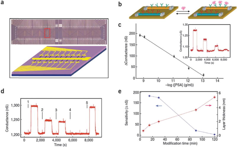
Nanowire sensor arrays and detector properties. (a) Optical image (top) of a nanowire device array. The white lines correspond to the silicon nitride passivated metal electrodes that connect to individual nanowire devices. The red rectangle highlights one of the repeated (vertical) regions where the nanowire devices are formed. The position of the microfluidic channel used to deliver sample is highlighted by the dashed white rectangle and has a total size of 6 mm × 500 mm, length × width. The image field is 8 mm × 1.2 mm. The schematic (bottom) shows details of metal electrodes (golden lines) connecting nanowires (blue lines) in this region with orientation rotated 90° relative to red rectangle. (b) Schematic showing two nanowire devices, 1 and 2, within an array, where the nanowires are modified with different (1, green; 2, red) antibody receptors. A cancer marker protein that binds specifically to its receptor (on nanowire-1) will produce a conductance change characteristic of the surface charge of the protein only on nanowire-1. (c) Change in conductance versus concentration of PSA for a p-type silicon nanowire modified with PSA-Ab1 receptor. Inset: conductance-versus-time data recorded after alternate delivery of PSA and pure buffer solutions; the PSA concentrations were 0.9 ng ml−1, 9 pg ml−1, 0.9 pg ml−1 and 90 fg ml−1, respectively. The buffer solutions used in all measurements were 1 mM phosphate (potassium salt) containing 2 mM KCl, pH = 7.4. (d) Conductance-versus-time data recorded for a PSA-Ab1-modified p-type silicon nanowire after alternate delivery of the following protein and pure buffer solutions: (1) 9 pg ml−1 PSA, (2) 0.9 pg ml−1 PSA, (3) 0.9 pg ml−1 PSA and 10 mg ml−1 BSA, (4) 10 mg ml−1 BSA and (5) 9 pg ml−1 PSA. (e) Thickness dependence (red curve) of aldehyde silane layer on the SiNW surfaces extracted from AFM measurements after different modification time of the aldehyde propyltrimethoxysilane, and sensitivity dependence (blue curve) of detection of 1 ng ml−1 of PSA, after different modification time using a p-type SiNW device. Copyright Nature Biotechnology, Nature Publications Group.38
Later, Lin et al. reported a highly sensitive and reusable silicon nanowire field-effect transistor for the detection of protein–protein interactions (Fig. 9).130 This reusable device was made possible by the reversible association of glutathione S-transferase-tagged calmodulin with a glutathione modified transistor. The calmodulin-modified transistor exhibited selective electrical responses to Ca (≥ 1 μM) and purified cardiac troponin I (~ 7 nM); the change in conductivity displayed a linear dependence on the concentration of troponin I in a range from 10 nM to 1 μM. The minimum concentration of Ca2+ required to activate calmodulin was determined to be 1 μM. The N-type Ca2+ channels, expressed by cultured 293T cells, can be recognized specifically by the calmodulin-modified nanowire transistor. This sensitive nanowire transistor can serve as a high-throughput biosensor and can also substitute for immune-precipitation methods used in the identification of interacting proteins.
Fig. 9.
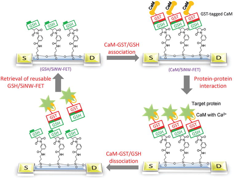
Schematic of the experimental approach. The strategy used in this study included the association of CaM-GST with a GSH/SiNW-FET to form the CaM/SiNW-FET complex, the subsequent detection of interacting proteins, and the removal of bound proteins via the dissociation of GSH-GST with 1 mM GSH washing solution. Copyright Proceedings of the National Academy of Sciences, National Academy of Sciences.130
The need for “bottom-up” Si-nanowire hybrid fabrication schemes results in severe integration issues that have hindered widespread application, and alternative “top-down” fabrication methods of nanowire-like devices produce disappointing performance because of process-induced material and device degradation. In order to overcome these limitations, Stern et al. used ultrathin silicon-on-insulator wafers,131 which require only lateral (in-plane, two-dimensional) active layer definition to achieve the nanometer dimensions needed for a nanowire-type device. An anisotropic wet etch fabrication process was established (Fig. 10 and 11). Specifically, tetramethylammonium hydroxide, TMAH, which etches Si(111) planes about 100 times more slowly than all other planes, allows retention of pattern definition, and smooths edge imperfections not aligned to the (111) plane. They have shown that these “nanowire” devices to be capable of monitoring antibody binding (limit of detection is less than 100 fM) and sensing the cellular immune response in real time. This approach should facilitate widespread diagnostic applications, and have potential for extension to a fully integrated system, with wide use as sensors in molecular and cellular arrays.
Fig. 10.
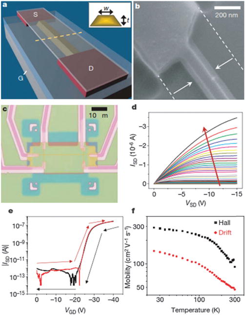
Device fabrication and electrical performance. (a) Schematic after anisotropic etch. The silicon-on-insulator active channel (yellow, width w and thickness t) is undercut etched, whereas degenerate leads (red) are etch resistant. The source (S), drain (D), and underlying back gate (G) are labelled. (b, c) Scanning electron micrograph (b) and optical micrograph (c) of a completed device. (d) ISD (VSD) (w = 50 nm, t = 25 nm) for varying VGS (0 to −40 V, ΔV = −1 V), illustrating p-type accumulation mode behaviour. (e) |ISD|(VGD) for VSD = 1 V for forward (red) and reverse (black) sweep. (f) Accumulation-mode Hall and drift mobilities versus temperature (w = 300 nm, t = 25 nm). Copyright Nature, Nature Publication Group.131
Fig. 11.
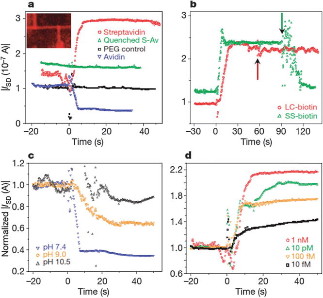
Protein detection and sensitivity. Solution exchange occurs at time zero. (a) Specific recognition and protein charge determination of avidin/ streptavidin. All additions used 1 nM solutions. Inset shows fluorescence micrograph of biotin-functionalized device after fluorescently labelled streptavidin addition. (b) Verification of surface charge by cleavage. Streptavidin (1 nM) addition to LC-biotin- or SS-biotin-functionalized devices. The arrow indicates reducing agent (TCEP) addition. (c) Biotinylated sensor response to protein charge, by addition of 1 nM avidin in buffers with different pH values. (d) Detection response with decreasing streptavidin concentration. For (c and d) currents were normalized by dividing the measured ISD by the pre-addition average current. Copyright Nature, Nature Publication Group.131
Gonçalves et al. described an α-Si:H-based ion-sensitive field-effect transistor (α -Si:H ISFET) used for the label-free detection of biological molecules.132 Threshold voltage shifts in the transfer curve of the ISFET are observed resulting from successive steps of surface chemical functionalization, covalent DNA attachment to the functionalized surface, surface blocking, and hybridization with a complementary target. The surface sensitivity achieved for DNA oligonucleotides is on the order of 1 pmol cm−2, and electronic detection of adsorbed proteins and DNA is also achieved by monitoring the shifts of the threshold voltage of the ISFETs, with a sensitivity of approximately 50 nM. Hakim et al. reported a polysilicon nanowire biosensor36 used to detect the proteins interleukin-8 (IL-8) and tumor necrosis factor-alpha (TNF- α) over a wide range of concentrations, demonstrating excellent sensitivity and selectivity (Fig. 12). A detection sensitivity of 10 fM in the presence of a 100 000-fold excess of a non-target protein can be achieved. Furthermore, nanowire titration curves gave antibody–antigen dissociation constants in good agreement with low-salt enzyme-linked immunosorbent assays (ELISAs). Additionally, their fabrication process produces high-quality nanowires that are suitable for low-cost mass production, providing a realistic route to the realization of disposable nano-electronic point-of-care devices. Kim et al. reported a first description of the detection of C-reactive protein (CRP) in human serum using a silicon-based biosensor,133 of which the limit of detection (LOD) determined from the standard curve was 0.1 ng ml−1, which is comparable to that of commercially available ELISAs. The detection range was also improved (0.1 ng ml−1 to 100 ng ml−1) compared to commercially available ELISAs.
Fig. 12.
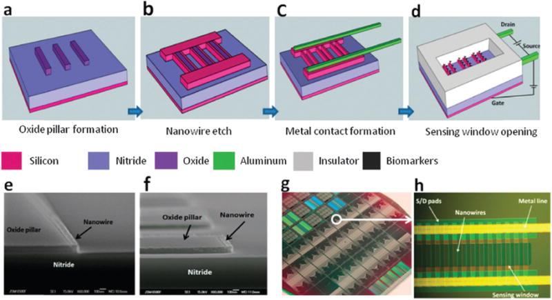
Schematic illustrations of polysilicon nanowire biosensor fabrication after (a) oxide pillar formation, (b) nanowire plasma etch, (c) metal contact formation, and (d) sensor window opening. The biasing configuration for the biosensor electrical measurements is also shown: (e) cross sectional SEM image of a fabricated polysilicon nanowire; (f) cross-sectional SEM micrograph of polysilicon nanowires at the corner of a pillar; (g) optical image of a completed nanowire biosensor wafer; (h) high magnification optical image of a fabricated nanowire biosensor through a sensor window. Copyright Nano Letters, ACS.36
Other inorganic semiconductors introduced for use in biosensors include GaN and SnO2. Cheng et al. reported using SnO2 nanobelts as a semiconductor;39 the devices with a single biotinylated SnO2 nanobelt showed pronounced conductance changes in response to streptavidin binding (Fig. 13). Importantly, the pH-dependence of the conductance changes was fully consistent with the charged states of streptavidin at different pH values. The sensor shows excellent selectivity, and they successfully applied it for detection of the cardiac troponin I (cTnI) subunit within cTn, a clinically important protein marker for myocardial infarction.
Fig. 13.
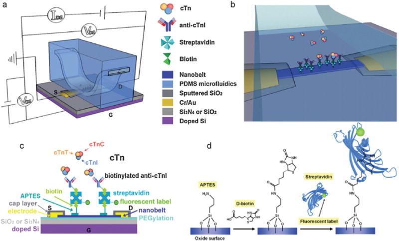
Schematic diagrams of the device structure, measurement configuration, sensing scheme and surface functionalization of SnO2 nanobelt cTnI within the cTn complex: (a) Schematic diagram of a SnO2 nanobelt FET device with integrated PDMS microfluidic channel, insulated electrodes and electrical measurement configuration. (b) A close-up schematic view of the cTnI sensing scheme at the antibody-functionalized nanobelt surface within the microfluidic channel. (c) Schematic diagram (not to scale) of the cTnI sensing scheme depicting the detailed assembly procedure of antibodies on the nanobelt surface and subsequent detection of the antigen. (d) Schematic diagrams for the nanobelt biotinylation process: step 1, covalent APTES linkage; step 2, biotinylation, and step 3, binding of fluorescently labeled streptavidin. Copyright Biosensors and Bioelectronics, Elsevier.39
Wen et al. used an AlGaN/GaN field effect transistor to fabricate highly sensitive biosensors with a control gate electrode for streptavidin detection.134 The device active area is functionalized with 3-aminopropyltriethoxysilane and N-hydroxysulfosuccinimide–biotin for streptavidin binding. With no resulting electrochemical side effects, a gate voltage is applied through a Pt control electrode to the solution so that the device can operate sensitively in the subthreshold regime. Due to the logarithmic relationship between the channel current and gate voltage in the subthreshold regime, at a concentration of 4.73 pM streptavidin the device exhibits 9.97% current change in the subthreshold regime compared with the current in phosphate buffered saline solution. In the linear regime, the current change is 0.49% at the same streptavidin concentration.
Importantly, Chang et al. group demonstrated an In2O3 nanowire-based biosensing system that is capable of performing rapid, label-free, electrical detection of cancer biomarkers directly from human whole blood collected by a finger prick.135 Passivating the nanowire surface successfully blocked the signal induced by nonspecific binding when performing active measurement in whole blood (Fig. 14). Passivated devices showed markedly smaller signals induced by nonspecific binding of proteins and other biomaterials in serum and higher sensitivity to target biomarkers than bare devices. The detection limit of passivated sensors for biomarkers (0.1 U mL−1 for CA-125 and 8 ng mL−1 for IGF-II, much lower than the clinically relevant level for diagnosis) in whole blood was similar to the detection limit for the same analyte in purified buffer solutions at the same ionic strength, suggesting minimal decrease in device performance in the complex media. Then they further demonstrated detection of multiple cancer biomarkers with high reliability at clinically meaningful concentrations from whole blood collected by a finger prick using this sensing system. The system developed here does not require any added reagents or sophisticated fabrication and is quite portable since it does not require any bulky equipment. This newly developed system consists of three parts: a sample processing system based on a custom-made microfilter, a sample delivery system based on a Teflon mixing cell, and a detection system based on the nanosensor array. This significant progress makes nanowire biosensors much close to real clinic applications.
Fig. 14.

Schematic diagrams of the device structure, responses to analyte at different concentrations. Copyright ACS Nano, ACS.135
Stern et al. also successfully achieved biomarker detection in physiological solution by using distinct components within the sensor to perform purification and detection.136 A microfluidic purification chip simultaneously captures multiple biomarkers from blood samples and releases them, after washing, into purified buffer for sensing by a silicon nanoribbon detector. This two-stage approach isolates the detector from the complex environment of whole blood, and reduces its minimum required sensitivity by effectively pre-concentrating the biomarkers, this resulted to a specific and quantitative detection of two model cancer antigens from a 10 μL sample of whole blood in less than 20 min (Fig. 15). This study marks the first use of label-free nanosensors with physiological solutions positioning this technology for rapid translation to clinical settings.
Fig. 15.
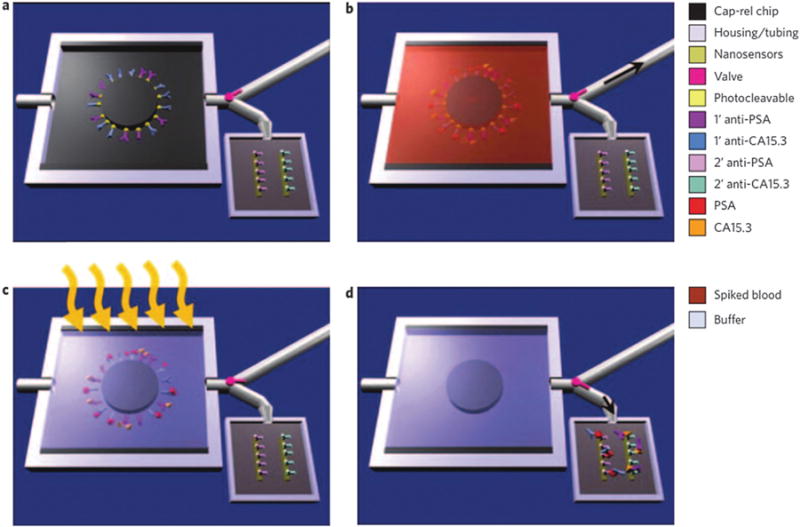
Schematic of MPC operation. (a) Primary antibodies to multiple biomarkers, here PSA and carbohydrate antigen 15.3 (CA15.3), are bound with a photo cleavable cross-linker to the MPC. The chip is placed in a plastic housing and a valve pink directs fluid flow exiting the chip to either a waste receptacle or the nanosensor chip. (b) Whole blood is injected into the chip with the valve set to the waste compartment (black arrow shows the direction of fluid flow) and, if present in the sample, biomarkers bind their cognate antibodies. (c) Washing steps follow blood flow, and the chip volume (5 μl) is filled with sensing buffer before UV irradiation (orange arrows). During UV exposure, the photolabile cross-linker cleaves, releasing the antibody–antigen complexes into solution. (d) The valve is set to the nanosensor reservoir (black arrow shows the direction of fluid flow) and the 5 μl volume is transferred, enabling label-free sensing to be performed to determine the presence of specific biomarkers. Copyright Nature Nanotechnology, Nature Publication Group.136
Two-dimensional carbon-based materials like carbon nanotubes, graphene, and carbon fibers, to be discussed later, have attracted the biosensor research community because of the high surface area to volume ratio that offers a relatively large active surface area. In the specific case of graphene, there is an unusually large background current owing to the zero band-gap. Wang et al. reported detection of a cancer marker protein down to 375 fM using a functionalized MoS2 nanosheet-based FET. As opposed to graphene, single MoS2 has a direct band gap, and thus the leakage current can be significantly decreased along with other advantages like decreased nonspecific binding due to electrostatic attractions.137 Later, Sarkar et al. had further improved the sensitivity of MoS2 FET sensor to about 100 fM, which surpasses the sensitivity of that based on graphene by more than 74-fold.138 Moreover, they establish through theoretical analysis that MoS2 is greatly advantageous for biosensor device scaling without compromising its sensitivity, which is beneficial for single molecular detection. (Fig. 16) Exploring other 2D inorganic materials might pave the way for further biosensor work.
Fig. 16.
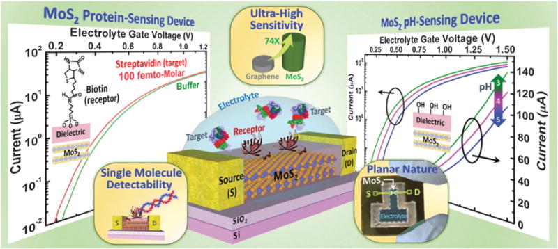
Schematic illustration of MoS2 FET based pH sensor and biosensor. Copyright ACS Nano, American Chemical Society.138
3.2. Organic semiconductors (OSCs)
OSCs have been intensively investigated over the last several decades with particular attention paid to their optoelectronic properties, resulting in a wide set of applications including OLEDs (organic light-emitting diodes) and OPVs (organic photovoltaics). This interest has been mainly due to the fact that this class of materials enjoys much greater tunability for optimizing its optoelectronic properties through chemical tailoring compared to other inorganic counterparts. Also, the possibility of introducing printing technology to achieve large area devices on various substrates (such as flexible PET or nano-paper) make OSCs highly attractive for low-cost high-efficient fabrication purposes.
Nevertheless, OSCs exhibit several drawbacks such as low charge carrier mobilities, inferior switch speeds, short operational lifetimes, and poor environmental stability compared with many inorganic analogs. Therefore, in order to take better advantage of these materials, it is wise to exploit their potential applications in circumstances in which the performances will not be limited by the above drawbacks, and the chemical sensitivity can be a bonus rather than a limitation.
Sensors are a particularly promising potential application for OSCs; high electronic circuit switching speeds are not required for sensors because the system response speed is limited by dynamic biochemical reactions and physical and chemical adsorption and desorption procedures at active sensing sites. More importantly, sensor sensitivity and selectivity can be optimized by controllably modifying OSC molecular structures. The potential to fabricate large area sensor devices on various flexible substrates using printing technology is highly interesting and attractive for wearable, conformable devices in particular.
3.2.1. Pentacene and its derivatives
Pentacene (structure shown with other representative OSCs in Scheme 2) is a frequently used semiconductor for biosensors due to its high mobility and stable performance. Khan et al. reported pentacene-based organic thin-film transistors as highly sensitive, real-time electronic sensors for selective antibody detection.139 Bovine serum albumin (BSA) was used as a receptor for detecting monoclonal anti-BSA by a label-free method (Fig. 17). This sensor can also discriminate protein charge changes over pH changes of the solution and determine the binding affinity of the antibody–antigen interaction. This provides an inexpensive, fast, and selective sensor platform for a wide range of applications in biomedical use, gene therapy, and microarrays, as well as screening for the affinity constant of specific antibodies generated by a library of cells.
Scheme 2.
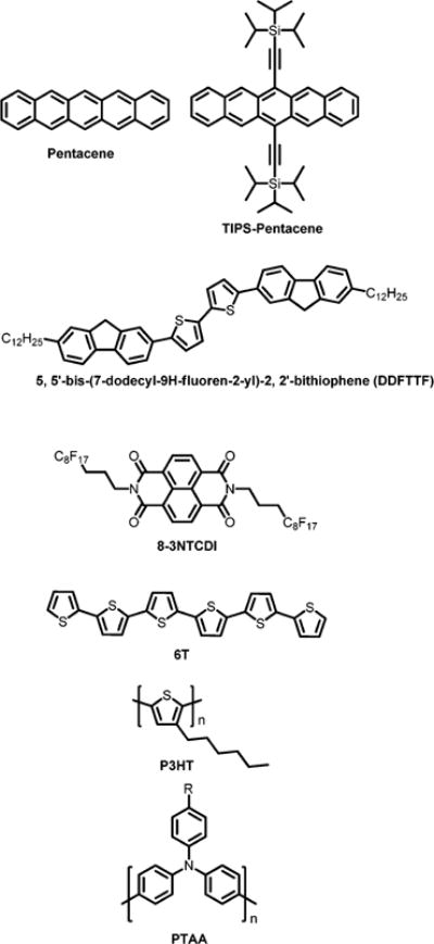
Chemical structures of semiconductors used in biochemical sensors.
Fig. 17.
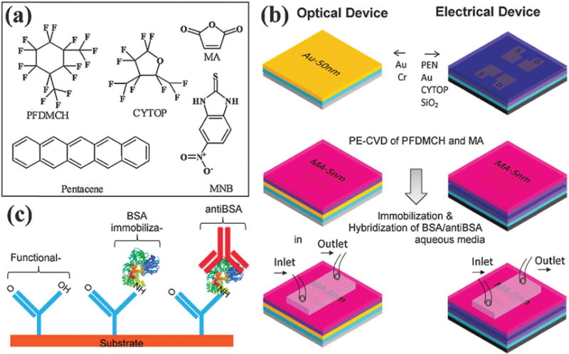
Schematic representation of a bottom-contact pentacene OTFT and optical sensors. (a) Chemical structure of the organic molecules. (b) (Right, top to bottom) fabrication procedure for a bottom-contact OTFT with CYTOP (15 nm)/SiO2 (200 nm) dielectric layer, source–drain electrodes with a W/L of 10 and a 30 nm pentacene layer followed by the top PE-CVD protective and functional layer. (Left, top to bottom) Fabrication procedure for the optical device with Au (50 nm)/Cr (2 nm)/LaSFN9 glass followed by the top identical PE-CVD protective and functional layer. (c) Schematics of the surface modification to immobilize the BSA for selective antiBSA detection. Copyright Journal of the American Chemical Society, American Chemical Society.139
Huang et al. introduced pentacene as a semiconductor for OFET sensors that can detect glial fibrillary acidic protein (GFAP)140 at a very high sensitivity. In this work, pentacene was also used as an element for the first inverter biosensor. Bonfiglio reported a highly sensitive and selective DNA-hybridization sensor based on TIPS-pentacene141 which can operate in an aqueous environment at ultralow voltages.
3.2.2. Other molecular semiconductors
5,5′-Bis-(7-dodecyl-9H-fluoren-2-yl)-2,2′-bithiophene (DDFTTF)
DDFTTF is another widely used p-type semiconductor for biochemical sensors due to its stability while operating in aqueous solutions. Its chemical structure is shown in Scheme 2. The long alkyl chain contributes to its excellent stability in water. OFETs were fabricated with this semiconductor (15 nm) on an ultra-thin (22 nm) cross-linked poly(vinyl phenol) polymer dielectric layer, leading to a device which can work below 1 V, a necessary requirement for stable operation in water and aqueous buffer solutions (Fig. 18). This semiconductor shows an average mobility value of 0.35 cm2 V−1 S−1 based on a top-contact OTFT architecture with channel width 4 mm and length 50 μm.142 Later, Hammock et al. introduced this semiconductor for protein detection by using nano-functionalized organic field-effect transistors. They demonstrated a detection limit of 100 pM for the protein with high selectivity over other proteases in situ.143
Fig. 18.
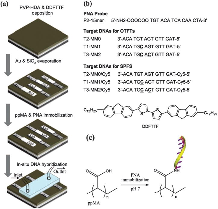
Schematic representation of the OTFT sensor fabrication. (a) Fabrication of OTFT with a PVP-HDA (20 nm) dielectric layer, DDFTTF organic semiconductor (15 nm), and source drain (S–D) electrodes with a W/L of 80. The interdigitated regions of the S–D electrodes were covered with thermally evaporated silicon monoxide and the entire device was functionalized With 5 nm pMA and a PNA probe. (b) PNA and DNA 15-mer sequences and the chemical structure of DDFTTF. Label-free DNA sequences were used for electrical detection with the OTFT sensors and sequences labeled with a Cy5 fluorophore were used for optical detection via SPFS. (c) Schematics of the surface modification to immobilize the PNA-15mer probe. Copyright Advanced Materials, Wiley.142
α-6T
α-6T is a prototypical organic semiconductor stable in an aqueous electrolyte, and it does not require any further surface passivation (Fig. 19). Buth et al. modified the α-6T surface by a controlled oxidation, which makes α-6T sensitive to the pH changes of the local aqueous solution. After further modifying the surface with (3-aminopropyl)triethoxysilane (APTES) and specific enzymes, they obtained sensors able to specifically detect penicillin in the μM range.144
Fig. 19.
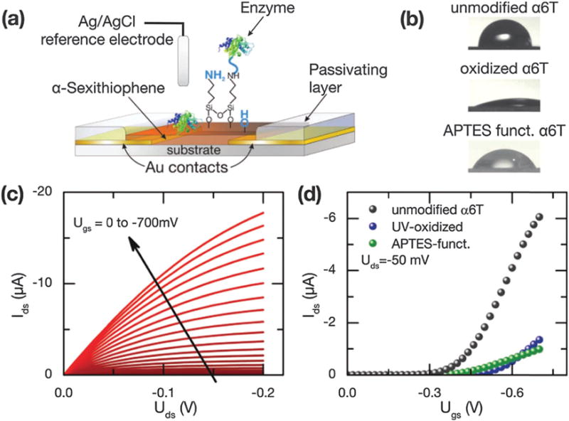
(a) Schematic drawing of the transistor layout, including the different functionalization steps investigated in this work. (b) Static water contact angle measurements of differently treated α-sexithiophene thin films. (c) Typical output characteristic of a transistor with a width-to-length ratio of 4900 recorded at pH 5. (d) Transfer curves of untreated, oxidized (5 min UV illumination) and APTES-functionalized transistors, measured at pH 5. Copyright Advanced Materials, Wiley.144
8-3 NTCDI
N-type semiconductors are rarely used in biomolecule sensors, probably due to the fact that most n-type semiconductors are unstable in aqueous solutions. Huang et al. successfully employed 8-3 NTCDI as a semiconductor for GFAP detection.140 In this work, 8-3 NTCDI could be stably operated in aqueous solutions with a high mobility and a large on/off ratio. This sensor’s limit of detection for GFAP is about 1 ng mL−1 (Fig. 20).
Fig. 20.
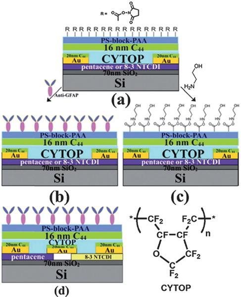
Device architecture of GFAP sensor: (a) activated carboxylate surface (b) anti-GFAP modified device; (c) hydroxyethylamide control device; (d) anti-GFAP modified inverter based on pentacene and 8–3 NTCD. Copyright Chemical Science, Royal Society of Chemistry.140
3.2.3. Polymer semiconductors
P3HT
P3HT is a widely-used p-type polymer semiconductor in OFET bio-chemical sensors due to its many advantageous properties including its usable hole mobility, chemical stability in aqueous solutions, and solution processability. Kergoat et al. reported a water-gated P3HT transistor for DNA detection,8 and this OFET device is able to work below 1 V. This work introduced a P3HT and P3PT–COOH mixed layer as the semiconductor as well as a DNA probe (ODN) linker. ODN was immobilized on semiconductor surface through 1-ethyl-3-(3-dimethylaminopropyl)carbodiimide-N-hydroxysuccinimide (EDC/NHS) chemistry. A drop of water was used as the gate, and clear changes in the output characteristic of the device were observed upon DNA immobilization and after DNA hybridization. Magliulo et al. also reported a similar electrolyte-gated OFET sensor.145 In this report, P3HT was employed as a semiconductor layer, and the surface of P3HT was treated by PE-CVD (plasma enhanced vapor chemical deposition), allowing deposition of a few nanometer-thick-coating rich in–COOH groups (Fig. 21). The –COOH groups were eventually used to stably anchor phospholipid molecules to the OSC surface. Biotin was subsequently attached for detecting streptavidin protein. A limit of detection of 10 nM was achieved.
Fig. 21.
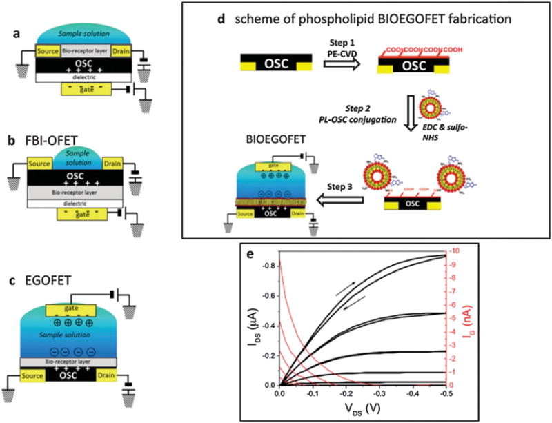
Schemes of the architectures of OFET biosensors proposed to date: (a) bi-layer OFET; (b) functional biological interlayer (FBI) OFET; (c) electrolyte-gated OFET (EGOFET). (d) Scheme of phospholipid BIOEGOFET fabrication. (e) Typical source–drain current–voltage characteristics (black curves, left ordinate) and gate currents (red curves, right ordinate) of a BIOEGOFET in presence of phosphate-buffered saline (PBS). Copyright Advanced Materials, Wiley.145
PTAA
Spijkman et al. used polytriarylamine (PTAA) as an OSC for a dual-gate OFET potentiometric sensor in aqueous solution.146 This OSC is stable at ambient conditions and yields reproducible transistors with a mobility of 10−3 cm2 V−1 s−1.
3.3. Carbon-based semiconductors and conductors
3.3.1. Carbon nanotubes
The connection between nanomaterials and biological systems has led to considerable progress for electronic biosensors. The integration of one-dimensional nanomaterials like nanowires into electronic devices offers substantial advantages for biomolecule sensing due to the large nanowire surface-to-volume ratio and similar dimensions of detector material domains and biological analytes. Organic one-dimensional nanomaterials, single-walled carbon nanotubes (SWNTs) in particular, show great potential for biomolecule detection. In the case of SWNTs, every atom is on the surface and exposed to the environment. Thus, even small environmental changes can cause drastic changes to SWNT electrical properties. Moreover, their all-carbon composition provides a natural match to organic molecules.41,43,45,147–149 Modification of SWNT surfaces by creating binding sites for anchoring receptor molecules is necessary for selective detection of target biomolecules. There are several approaches for SWNT surface modification: (a) coating SWNTs with poly(ethylene imine) (PEI) and poly(ethylene glycol) (PEG) (used to reduce non-specific adsorption), then coupling with receptor molecules through EDC/NHS based bio-conjugation reaction; (b) bridging SWNT and receptor molecules with 1-pyrenebutanoic acid succinimidyl ester; the pyrene group having strong π–π interaction with the SWNT surface while the succinimidyl ester group chemically reacts with the receptor; (c) treating SWNT with a diazonium salt of a carboxylic acid to create sp3 hybridized sites, then activating the carboxylic acid group with EDC, stabilizing it with NHS, then anchoring the receptor through a covalent bond formation.
SWNT FETs can be used for many applications such as detection of antibody–antigen interactions, glucose sensing, and DNA hybridization sensing. After modifying the SWNT surface with target biomolecule recognition (receptor) layers, specific detection of target analytes can be achieved. Allen et al. accomplished a highly sensitive detection of streptavidin through biotin functionalized carbon nanotubes,41 which bridged two microelectrodes (source and drain). PEI and PEG were first coated on a SWNT: PEI was used to anchor receptors as discussed before, while PEG was used to reduce nonspecific adsorption of biomolecules to the SWNT. The source–drain current of the SWNT FET shows a significant decrease upon the streptavidin binding to the biotin-functionalized carbon nanotubes. AFM imaging also confirmed the binding of streptavidin with the biotin-functionalized SWNT device (Fig. 22).
Fig. 22.
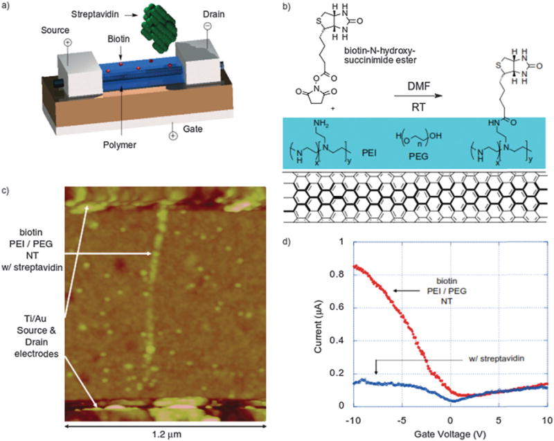
(a) Schematic illustration of an NTFET coated with a biotinylated polymer layer for specific streptavidin binding. (b) Biotinylation reaction of the polymer layer (poly(ethylene imine)/poly(ethylene glycol) (PEI/PEG)) on the sidewall of the SWNT. (c) Atomic force microscopy image of the polymer-coated and biotinylated NTFET device after exposure to streptavidin labeled with gold nanoparticles (10 nm in diameter). (d) The source–drain current dependence on the gate voltage of the NTFET device based on SWNT functionalized with biotin in the absence and presence of streptavidin. DMF: dimethylformamide. RT: room temperature. Copyright Advanced Materials, Wiley.41
Lerner et al. developed a novel detection method for osteopontin (OPN), a new biomarker for prostate cancer, by attaching a genetically engineered single-chain variable fragment (scFv) proteins with high binding affinity for OPN to a carbon nanotube field-effect transistor (NT-FET).45 A concentration-dependent increase in the source–drain current is observed in the regime of clinical significance, with a detection limit of approximately 30 fM. Furthermore, this NT-FET device also shows good selectivity for OPN over other control proteins. Li et al.150 studied the complementary detection of prostate-specific antigen (PSA) by using a network of SWNTs in a FET. A very low limit of detection was ca. 500 pg mL−1, or 14 pM, at a signal-to-noise ratio of 2. This sensitivity is comparable to that obtained from metal oxide nanowires (Fig. 23).
Fig. 23.
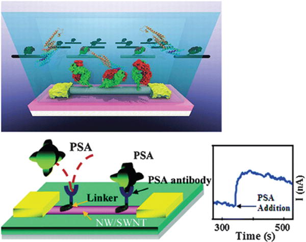
Top: osteopontin (OPN) and bottom: (prostate-specific antigen) PSA sensor platform based on carbon nanotube. Copyright Journal of the American Chemical Society, American Chemical Society.150
While DNA hybridization accompanied by electrostatic interactions and charge transfer can be detected by NTFET devices, the exact mechanism of the detection remains unclear. DNA molecules could attach to different segments of SWNT devices. If DNA molecules attach to the SWNT, they will mostly affect FET characteristics by electron depletion in the channel, while if DNA molecules chemically attach to metal electrodes, they will influence only the metal/nanotube interface, that is, the Schottky barrier. As a result, by correlating the sensing results to the attachment mode, we can obtain information about the mechanism of SWNT FET biosensing.
Maehashi et al. covalently immobilized peptide nucleic acid (PNA) oligonucleotides onto the SWNT FET back-gated Au surfaces,151 and the electrical properties of the SWNT devices were measured at room temperature in air. First, the blank phosphate-buffered saline (PBS) solution was introduced into the poly(dimethylsiloxane) (PDMS)-based micro flow chip, and no substantial change in the source–drain current of the SWNT FET was observed. After 3 hours of real time monitoring, the current dramatically increased due to the negative surface charge density associated with binding of negatively charged oligonucleotides at the surface of p-type SWNT FET. DNA hybridization can be detected by measuring the electrical characteristics of the SWNT FET. Therefore, SWNT FET devices can be introduced for label-free, direct real time electrical detection of biomolecule binding.
3.3.2. Graphene
Graphene, a single layer of graphite, is an ideal two-dimensional crystal showing extremely high mobility of ~104 cm2 V−1 s−1 and large carrier density of 1012 cm−2 at room temperature without doping, making it operable at very low electrical field and thus avoiding biomolecule oxidation during analysis. Furthermore, because its electrical characteristics are highly sensitive to surface conditions, graphene is attractive for biomolecule detection in aqueous solutions. Ohno et al. reported electrolyte-gated graphene field-effect transistors (GFETs) for electrically detecting both pH and protein adsorptions.152 They noticed that graphene conductance exhibited a direct linear correlation with electrolyte pH, and the conductance increased with exposure to a protein at several hundred picomolar.
Park et al. reported another biomolecule sensor based on graphene.46 O2 plasma- and NH3 plasma-treated flexible bilayer graphene were used as semiconductors, which can work at low driving voltage. The human olfactory receptor 2AG1 (hOR2AG1: OR) was immobilized on graphene surface through glutaraldehyde (GA) and 1,5-diaminonaphthalene (DAN). DAN was stacked on the side plane of the MBLG by π–π interactions between the naphthalene group of DAN and its sp2-carbon plane, in order to immobilize OR on the MBLGs. Glutaraldehyde (GA) was also added, and the GA-conjugated DAN/MBLG was formed through a Schiff-base reaction. Finally, through similar chemistry, a covalent bond was formed between the amine group of the OR and the aldehyde group of the GA–DAN/MBLG. The resulted B-noses are ultrasensitive and highly selective toward amyl butyrate (AB), with a minimum detection limit (MDL) of 0.04 fM (10−15; signal-to-noise: 4.2). Furthermore, this B-nose has long-term stability and excellent mechanical bending durability in flexible systems (Fig. 24).
Fig. 24.

Illustration of OR-conjugated B-Nose and its sensing behavior. Copyright Nano Letters, American Chemical Society.46
Though significant progresses had been made to broaden the semiconductor materials range and develop low cost, printable, flexible and reliable semiconductors for bio-molecule detection in recent years, it is still highly challenging to detect target biomarkers in physiological solutions or whole blood samples, because of problems such as biofouling, non-specific binding, and the ion screening effect discussed above. So far, the most reliable systems for field-effect bio-molecule detection seem to be based on inorganic nanowire semiconductors due to their large surface to volume ratio, excellent electrical performance as well as ultrahigh sensitivity. More importantly, inorganic nanowire semiconductors can detect target bio-markers in whole blood samples or physiological solutions.38,134,135
Carbon nanotube biosensors also show some reliability for protein, DNA, and glucose detection. Detection of biomarkers in real physiological solutions was also achieved. For example, the Rusling group reported the combination of electrochemical immunosensors using single-wall carbon nanotube (SWNT) forest platforms with multi-label secondary antibody–nanotube bioconjugates for highly sensitive detection of a cancer biomarker in serum and tissue lysates;153 a detection limit of 4 pg mL−1 for prostate specific antigen in 10 μL of undiluted calf serum was achieved. This result is promising for clinical screening of cancer biomarkers and point-of-care diagnostics. However, several technical issues have to be resolved to further miniaturize and multiplex SWNT-FET biosensors: first, preventing non-specific adsorption of biomolecules onto the tube walls; second, the underlying bio-detection mechanism needs to be thoroughly understood; third, the noise in SWNT-FET electrical signals needs to be resolved to acquire ultralow detection limits in miniaturized SWNT-FET biosensors. Future efforts should be more strongly devoted to make more semiconductors (particularly printable organic semiconductors) reliably operate in whole blood samples or untreated physiological solutions; this is the key step to achieving low-cost point-of-care FET sensors.
4. Dielectric layers for top gated biomolecule sensors
For top-gated biomolecule sensors, it is necessary that the dielectric layer functions as both a dielectric layer and as a passivation layer. A high capacitance is necessary to transduce surface charge density change to the OFET channel and lead to sensitive detection of target molecules. Furthermore, this dielectric layer should also be able to prevent water and ions from penetrating and diffusing into the semiconductor layer; the failure of this function may lead to severe doping of the semiconductor and cause significant noise. Additionally, water and ion doping will drastically damage the OFET device through hydrolytic chemistry, electrolysis, and delamination. It should be noted that many inorganic semiconductors are associated with native or intentionally grown dielectric oxides that serve as top dielectrics, often with little additional chemical design or processing required.
4.1. Hydrophobic polymers
Fluorinated polymers and oligomers are well suited for top-gated OFET sensor dielectric layers. Khan et al. used PFDMCH (fluorinated polymer structures shown in Scheme 3 and Fig. 17 discussed above) as such a layer,139 which shows excellent signal transducing ability and good passivation functionality. Based on this dielectric layer, this sensor can sensitively detect anti-BSA and unambiguously discriminate the hybrid anti-BSA charges at different pH values. Furthermore, this sensor displays a high affinity constant (KA) of (1.1 ± 3) × 107 M−1 at pH 7, which is 1 order of magnitude higher than those obtained with a highly sensitive surface plasmon resonance spectroscopy detection system.
Scheme 3.

Chemical structure of insulating materials used as top dielectric layers.
CYTOP is another frequently used polymer for a top dielectric layer. However, a CYTOP thin film alone shows poor passivation ability due to pinholes embedded in the film. Therefore, the addition some hydrophobic small molecules to fill up these pinholes can greatly improve the passivation ability of CYTOP film. Huang et al. reported using C44H90 to fill pinholes on CYTOP films,140 and the resulted film showed excellent passivation effect. The resulting functionalized device shows high sensitivity to GFAP (Fig. 20). Spijkman et al. reported using PIBMA–teflon as a top dielectric layer for pH sensing.146 PIBMA–teflon mix layers show excellent passivation effect, and the sensitivity to pH is proportional to the ratio of C(top dielectric)/C(bottom dielectric).
Magliulo et al. reported a novel phospholipid passivation layer as a top gate dielectric layer.145 Phospholipid layers are versatile bio-systems that are the main components of biological membranes (Fig. 21 discussed above). They are amphipathic molecules and spontaneously self-assemble in water, forming bilayers facing the outer aqueous domains with their hydrophilic moiety and secluding in the interior of the bilayer the two hydrophobic acyl chains. Being formed by a non-polar oil-like inner part, the phospholipid layer bilayers display a capacitance of around 1 μF cm−2. This phospholipid layer was anchored on the FET surface by –COOH groups on the device. The non-polar nature of the deposited phospholipid bilayer interior minimized ionic diffusion through the membrane, eventually limiting the OSC doping, and the biotinylated phospholipid layer conveniently furnished binding sites for streptavidin- or avidin-capturing proteins. As a result, this transistor sensor reached the low limit of detection value of 10 nM.
4.2. Polar gating materials
Electrolytes can serve as the medium to electronically separate the gate from the transistor channel, allowing low-voltage operation. In particular, electrolytes have attracted much recent attention since they generate very high electric fields at the organic transistor channel/electrolyte interface at very low voltage, i.e., below 1 V. Kergoat et al. used pure water as top dielectric layer,8 and demonstrated that this water-gated device operated entirely in the field-effect mode of operation. This result shed new light on low-voltage operating OFETs, their charge transport characteristics under exposure to water, and sensor applications using water-gated OFETs as transducers in aqueous media. Additionally, due to the simplicity and readiness of its production, it could also reveal a very helpful tool for rapid testing of new organic semiconductor compounds. Finally, by using this water gated transistor, the Horowitz group observed clear changes in the output characteristic of the device upon DNA immobilization and after DNA hybridization (Fig. 25).
Fig. 25.
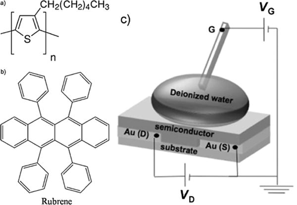
The chemical structures for (a) P3HT and (b) rubrene. (c) Schematic view of the water-gated organic transistor. Copyright Advanced Materials, Wiley.8
The previous two sections summarized material options for conductometric and field-effect biosensors. In addition, the impedance changes (both resistance and capacitance) generated in and around the dielectric materials can be directly measured as a further signaling option. While outside the scope of this review, “active” dielectrics into which bioanalytes can penetrate and perhaps undergo electrochemistry154,155 bridge the gap between biosensors where analytes interact directly with semiconductors and electrodes, and where analytes are completely isolated by the dielectrics from the semiconducting and conducting elements of the devices.
5. Maximizing signal strength and signal/noise ratio
5.1. Architecture approaches to improving field-effect biosensor signals
To obtain useful electrical signals from field-effect biosensors, it will be necessary to increase the intensity and stability of detection indicators, decrease noise interference, and filter out responses caused by nonspecific binding. Electronic engineering approaches to doing this involve both the individual sensor architecture and the design of circuits in which the sensors are embedded.
5.2. Increasing the signal via modification of FET structure or detection mechanism
Pei-Wen et al. reported a polysilicon nanowire FET based biosensor to detect cardiac-specific troponin-1 concentration in blood serum.156 Sixteen-fold enhancement of the biosensor response has been reported by introducing an external electric field via bottom gate, during the incubation stage of the protein on the sensor, leading to increased electrostatic attraction between the analyte and active area of the sensor. Non-specific binding interaction was much less probable even after enhanced concentration in the vicinity of the active surface. To minimize the effect of process variation and other environmental sources of noise, a Wheatstone bridge architecture was employed with the resistive biosensors as the four arms. The circuitry consist of a low noise analog front end, a 10 bit analog to digital converter, an on off key wireless transceiver to facilitate the processing of the signal generated by the biosensor cell (commercial fabrication process employed). Two order magnitudes higher sensitivity then commercially used Eliza technique was achieved using the described design.
In a unique approach to resolving the low frequency noise issue for sensitivity, Li et al. used the trapping behavior in nanowires for generating highly sensitive response signals.157 Trapping and detrapping of the charges in oxide traps has been established as the major reason for current fluctuation in nanowires, but by decreasing the nanowire dimension it is possible to achieve a system where only a single trap is responsible for current fluctuation. Thus, the drain current would have two distinct states with characteristic time constants corresponding to trapping and detrapping. The capture time constant has been related to the surface potential, which in turn is determined by the pH of the gating electrolyte solution. Sensitivity extracted using the trapping time constant was reported to be 400% more sensitive than monitoring the drain current.
Shoorideh et al. discussed the importance of proper operational range for optimal sensitivity. Operation of fully depleted FET based biosensor with an engineered amount of surface charge in the oxide layer near the electrolyte and oxide interface gives the maximum sensitivity. These conditions ensure lower Debye screening and optimal sub threshold swing resulting in maximizing the biosensor response.158
5.3. Enhancements through circuit elements and design
Takihi et al. proposed a charged-conserved analog-to-digital converter with a sensor cell and the pulse processing circuit. The proposed system eliminates the issue of thermal noise arising from voltage sources when supply or signal voltage is low in the case of a voltage domain signal. This system also avoids the issue of the signal distortion due to bit line capacitance as in the case of conventional voltage-pulse-based time-domain output signals. This design consists of a sensor cell and a pulse-processing unit. In this array, instead of a voltage signal, a current pulse is propagated through the sensor cell, keeping the charge on the bitline capacitance fixed by keeping the bitline voltage fixed. This results in more energy efficient, improved dynamic range with faster processing speed. The sensor cell consists of four transistors. A wordline is employed for selecting the senor cell while a bitline is used for the output signal propagation. For fixing the bitline voltage, the pulse processing unit consist of an opamp and three transistors for regulating a cascade amplifier. For converting the current pulse to voltage pulse there is a mirror current which gives a rail-to-rail voltage output. Finally a time to digital converter converts the PPC output voltage to binary output. The proposed circuit can be utilized to decrease the noise level in signal transduction and processing, and it also has a factor of ten lower energy footprint.159
Arya et al. emphasized the implications of proper functionalization of the active surface and the electrode geometries in enhancing the sensitivity of the biosensor platform. They demonstrated a microdisk electrode array treated with dithiobis self-assembled monolayer that gave better signal resolution, while a macroelectrode with a comb structure when functionalized with dithiobis(succinimidyl propionate) (DSP) in acetone with NaBH4 gave a 15-fold increase in biosensing response. Switching the electrode geometries and the treatments resulted in decreasing the signal clarity and response.160 Hence, specific details like electrode size and associated functionalization steps can play a very crucial role in improving biosensor sensitivity.
One approach to amplification of sensor signals is the use of multiple sensitive circuit elements in a single component. Huang and Besar, based on precedents by Tremblay,161 incorporated a p-type and n-type responsive transistor in series in an inverter geometry.140 The responses of the two transistors acted synergistically to create an inversion voltage difference in the presence of GFAP.
6. Summary and outlook
In summary, we have presented recent progress on field-effect biochemical sensors, including the biomolecule interactions that produce local electric fields, structures and processes at interfaces between bioanalyte solutions and electronic materials, semiconductors used in biochemical sensors, dielectric layers used in top-gated sensors, and mechanisms for converting the surface voltage change to higher signal/noise outputs in circuits. Progress in all of these areas makes OFET sensors highly promising for real applications. It is expected that future efforts will expand the range of novel materials and device structures for improvements in the standard parameters such as sensitivity and selectivity. However, a particularly important challenge is to improve sensor operation on real physiological samples, such as untreated blood and other body fluids, with calibration by more mature technologies and assurance of good statistical reproducibility under such conditions. The protein, carbohydrate, and salt concentrations in such samples can lead to greatly altered responses. Attaining sensitivity to analytes of interest in the presence of the components of real biological media is the key step to bring this technology out of the laboratory.
Acknowledgments
We thank the Flextech Alliance and the Johns Hopkins Institute for Clinical and Translational Research for support of this work. J.L.D. acknowledges the National Science Foundation for a Graduate Fellowship.
References
- 1.Luo X, Davis JJ. Chem Soc Rev. 2013;42:5944–5962. doi: 10.1039/c3cs60077g. [DOI] [PubMed] [Google Scholar]
- 2.Mehrabani S, Maker AJ, Armani AM. Sensors. 2014;14:5890–5928. doi: 10.3390/s140405890. [DOI] [PMC free article] [PubMed] [Google Scholar]
- 3.Torsi L, Magliulo M, Manoli K, Palazzo G. Chem Soc Rev. 2013;42:8612–8628. doi: 10.1039/c3cs60127g. [DOI] [PubMed] [Google Scholar]
- 4.Chen K, Li B, Chen Y. Nano Today. 2011;6:131–154. [Google Scholar]
- 5.Cotrone S, Cafagna D, Cometa S, De Giglio E, Magliulo M, Torsi L, Sabbatini L. Anal Bioanal Chem. 2012;402:1799–1811. doi: 10.1007/s00216-011-5610-2. [DOI] [PMC free article] [PubMed] [Google Scholar]
- 6.Hu P, Zhang J, Li L, Wang Z, O’Neill W, Estrela P. Sensors. 2010;10:5133–5159. doi: 10.3390/s100505133. [DOI] [PMC free article] [PubMed] [Google Scholar]
- 7.Joshi RK, Schneider JJ. Chem Soc Rev. 2012;41:5285–5312. doi: 10.1039/c2cs35089k. [DOI] [PubMed] [Google Scholar]
- 8.Kergoat L, Herlogsson L, Braga D, Piro B, Pham MC, Crispin X, Berggren M, Horowitz G. Adv Mater. 2010;22:2565–2569. doi: 10.1002/adma.200904163. [DOI] [PubMed] [Google Scholar]
- 9.Lin P, Yan F. Adv Mater. 2012;24:34–51. doi: 10.1002/adma.201103334. [DOI] [PubMed] [Google Scholar]
- 10.Sarkar T, Gao Y, Mulchandani A. Appl Biochem Biotechnol. 2013;170:1011–1025. doi: 10.1007/s12010-013-0233-z. [DOI] [PubMed] [Google Scholar]
- 11.Zhang GJ, Ning Y. Anal Chim Acta. 2012;749:1–15. doi: 10.1016/j.aca.2012.08.035. [DOI] [PubMed] [Google Scholar]
- 12.Zhou Y, Chiu CW, Liang H. Sensors. 2012;12:15036–15062. doi: 10.3390/s121115036. [DOI] [PMC free article] [PubMed] [Google Scholar]
- 13.Sun J, Zhang B, Katz HE. Adv Funct Mater. 2011;21:29–45. [Google Scholar]
- 14.Marks TJ. Acc Chem Res. 2011;44:501–510. doi: 10.1021/ar200006r. [DOI] [PubMed] [Google Scholar]
- 15.Wang C, Dong H, Hu W, Liu Y, Zhu D. Chem Rev. 2012;112:2208–2267. doi: 10.1021/cr100380z. [DOI] [PubMed] [Google Scholar]
- 16.Kola S, Sinha J, Katz HE. J Polym Sci, Part B: Polym Phys. 2012;50:1090–1120. [Google Scholar]
- 17.Facchetti A. Chem Mater. 2011;23:733–758. [Google Scholar]
- 18.Klauk H. Chem Soc Rev. 2010;39:2643–2666. doi: 10.1039/b909902f. [DOI] [PubMed] [Google Scholar]
- 19.Guo Y, Yu G, Liu Y. Adv Mater. 2010;22:4427–4447. doi: 10.1002/adma.201000740. [DOI] [PubMed] [Google Scholar]
- 20.Braga D, Horowitz G. Adv Mater. 2009;21:1473–1486. [Google Scholar]
- 21.McCarthy MA, Liu B, Donoghue EP, Kravchenko I, Kim DY, So F, Rinzler AG. Science. 2011;332:570–573. doi: 10.1126/science.1203052. [DOI] [PubMed] [Google Scholar]
- 22.Myny K, Steudel S, Smout S, Vicca P, Furthner F, Putten Bvander, Tripathi aK, Gelinck GH, Genoe J, Dehaene W. Org Electron. 2010;11:1176–1179. [Google Scholar]
- 23.Huang J, Dawidczyk TJ, Jung BJ, Sun J, Mason AF, Katz HE. J Mater Chem. 2010;20:2644. [Google Scholar]
- 24.Sokolov N, Bettinger CJ, Bao Z. Acc Chem Res. 2012;45:361–371. doi: 10.1021/ar2001233. [DOI] [PubMed] [Google Scholar]
- 25.Kim J, Nga Ng T, Soo Kim W. Appl Phys Lett. 2012;101:103308. [Google Scholar]
- 26.Angione MD, Cotrone S, Magliulo M, Mallardi A, Altamura D, Giannini C, Cioffi N, Sabbatini L, Fratini E, Baglioni P, Scamarcio G, Palazzo G, Torsi L. Proc Natl Acad Sci U S A. 2012;109:6429–6434. doi: 10.1073/pnas.1200549109. [DOI] [PMC free article] [PubMed] [Google Scholar]
- 27.Horowitz G. Adv Mater. 1998;10:365–377. [Google Scholar]
- 28.Horowitz G, Hajlaoui R, Bouchriha H. Adv Mater. 1998;10:923–927. [Google Scholar]
- 29.Horowitz G. Synth Met. 1999;101:401–404. [Google Scholar]
- 30.Horowitz G. J Mater Res. 2011;19:1946–1962. [Google Scholar]
- 31.Horowitz G, Lang P, Mottaghi M, Aubin H. Adv Funct Mater. 2004;14:1069–1074. [Google Scholar]
- 32.Sirringhaus H. Adv Mater. 2005;17:2411–2425. [Google Scholar]
- 33.Zaumseil J, Sirringhaus H. Chem Rev. 2007;107:1296–1323. doi: 10.1021/cr0501543. [DOI] [PubMed] [Google Scholar]
- 34.Newman CR, Frisbie CD, Demetrio A, Filho S, Bre J. Chem Mater. 2004;16:4436–4451. [Google Scholar]
- 35.Dhar BM, Ozgun R, Dawidczyk T, Andreou A, Katz HE. MSE Reports. 2011;72:49–80. [Google Scholar]
- 36.Hakim MMA, Lombardini M, Sun K, Giustiniano F, Roach PL, Davies DE, Howarth PH, De Planque MRR, Morgan H, Ashburn P. Nano Lett. 2012;12:1868–1872. doi: 10.1021/nl2042276. [DOI] [PubMed] [Google Scholar]
- 37.Lin TW, Hsieh PJ, Lin CL, Fang YY, Yang JX, Tsai CC, Chiang PL, Pan CY, Chen YT. Proc Natl Acad Sci U S A. 2010;107:1047–1052. doi: 10.1073/pnas.0910243107. [DOI] [PMC free article] [PubMed] [Google Scholar]
- 38.Zheng G, Patolsky F, Cui Y, Wang WU, Lieber CM. Nat Biotechnol. 2005;23:1294–1301. doi: 10.1038/nbt1138. [DOI] [PubMed] [Google Scholar]
- 39.Cheng Y, Chen KS, Meyer NL, Yuan J, Hirst LS, Chase PB, Xiong P. Biosens Bioelectron. 2011;26:4538–4544. doi: 10.1016/j.bios.2011.05.019. [DOI] [PubMed] [Google Scholar]
- 40.Sekitani T, Someya T. Adv Mater. 2010;22:2228–2246. doi: 10.1002/adma.200904054. [DOI] [PubMed] [Google Scholar]
- 41.Allen BL, Kichambare PD, Star A. Adv Mater. 2007;19:1439–1451. [Google Scholar]
- 42.Heller I, Janssens AM, Männik J, Minot ED, Lemay SG, Dekker C. Nano Lett. 2008;8:591–595. doi: 10.1021/nl072996i. [DOI] [PubMed] [Google Scholar]
- 43.Kim SN, Rusling JF, Papadimitrakopoulos F. Adv Mater. 2007;19:3214–3228. doi: 10.1002/adma.200700665. [DOI] [PMC free article] [PubMed] [Google Scholar]
- 44.Kuang Z, Kim SN, Crookes-goodson WJ, Farmer BL, Naik RR. ACS Nano. 2010;4:452–458. doi: 10.1021/nn901365g. [DOI] [PubMed] [Google Scholar]
- 45.Lerner MB, D’Souza J, Pazina T, Dailey J, Goldsmith BR, Robinson MK, Johnson ATC. ACS Nano. 2012;6:5143–5149. doi: 10.1021/nn300819s. [DOI] [PMC free article] [PubMed] [Google Scholar]
- 46.Park SJ, Kwon OS, Lee SH, Song HS, Park TH, Jang JJ. Nano Lett. 2012;12:5082–5090. doi: 10.1021/nl301714x. [DOI] [PubMed] [Google Scholar]
- 47.Schöning MJ, Poghossian A. Analyst. 2002;127:1137–1151. doi: 10.1039/b204444g. [DOI] [PubMed] [Google Scholar]
- 48.Mabeck JT, Malliaras GG. Anal Bioanal Chem. 2006;384:343–353. doi: 10.1007/s00216-005-3390-2. [DOI] [PubMed] [Google Scholar]
- 49.Thompson LA, Kowalik J, Josowicz M, Janata J. J Am Chem Soc. 2003;125:324–325. doi: 10.1021/ja027929z. [DOI] [PubMed] [Google Scholar]
- 50.Bunimovich YL, Shin YS, Yeo W, Amori M, Kwong G, Heath JR. J Am Chem Soc. 2006;128:16323–16331. doi: 10.1021/ja065923u. [DOI] [PMC free article] [PubMed] [Google Scholar]
- 51.Lai S, Demelas M, Casula G, Cosseddu P, Barbaro M, Bonfiglio A. Adv Mater. 2013;25:103–107. doi: 10.1002/adma.201202996. [DOI] [PubMed] [Google Scholar]
- 52.You X, Pak JJ. Sens Actuators, B. 2014;202:1357–1365. [Google Scholar]
- 53.Besteman K, Lee J, Wiertz FGM, Heering HA, Dekker C. Nano Lett. 2003;3:727–730. [Google Scholar]
- 54.Caras S. Anal Chem. 1980;52:1935–1937. [Google Scholar]
- 55.Grieshaber D, MacKenzie R, Voeroes J, Reimhult E. Sensors. 2008;8:1400–1458. doi: 10.3390/s80314000. [DOI] [PMC free article] [PubMed] [Google Scholar]
- 56.McKinley BA. Chem Rev. 2008;108:826–844. doi: 10.1021/cr068120y. [DOI] [PubMed] [Google Scholar]
- 57.Mu L, Droujinine I, Rajan N, Sawtelle S, Reed M. Nano Lett. 2014:5315–5322. doi: 10.1021/nl502366e. [DOI] [PubMed] [Google Scholar]
- 58.You X, Pak JJ. Sens Actuators, B. 2014;202:1357–1365. [Google Scholar]
- 59.Sohn IY, Kim DJ, Jung JH, Yoon OJ, Thanh TN, Quang TT, Lee NE. Biosens Bioelectron. 2013;45:70–76. doi: 10.1016/j.bios.2013.01.051. [DOI] [PubMed] [Google Scholar]
- 60.Kharitonov AB, Zayats M, Lichtenstein A, Katz E, Willner I. Sens Actuators, B. 2000;70:222–231. [Google Scholar]
- 61.Jang HJ, Ahn J, Kim MG, Shin YB, Jeun M, Cho WJ, Lee KH. Biosens Bioelectron. 2015;64:318–323. doi: 10.1016/j.bios.2014.09.020. [DOI] [PubMed] [Google Scholar]
- 62.Lerner MB, D’Souza J, Pazina T, Dailey J, Goldsmith BR, Robinson MK, Johnson ATC. ACS Nano. 2012;6:5143–5149. doi: 10.1021/nn300819s. [DOI] [PMC free article] [PubMed] [Google Scholar]
- 63.Eteshola E, Keener MT, Elias M, Shapiro J, Brillson LJ, Bhushan B, Lee SC. J R Soc, Interface. 2008;5:123–127. doi: 10.1098/rsif.2007.1107. [DOI] [PMC free article] [PubMed] [Google Scholar]
- 64.Jun J, Lee JS, Shin DH, Jang J. ACS Appl Mater Interfaces. 2014:13859–13865. doi: 10.1021/am5032693. [DOI] [PubMed] [Google Scholar]
- 65.Ohtake T, Hamai C, Uno T, Tabata H, Kawai T. Jpn J Appl Phys. 2004;43:L1137–L1139. [Google Scholar]
- 66.Vu XT, GhoshMoulick R, Eschermann JF, Stockmann R, Offenhaüsser A, Ingebrandt S. Sens Actuators, B. 2010;144:354–360. [Google Scholar]
- 67.Buth F, Donner A, Sachsenhauser M, Stutzmann M, Garrido JA. Adv Mater. 2012;24:4511–4517. doi: 10.1002/adma.201201841. [DOI] [PubMed] [Google Scholar]
- 68.Lin P, Yan F. Adv Mater. 2012;24:34–51. doi: 10.1002/adma.201103334. [DOI] [PubMed] [Google Scholar]
- 69.Mena M, Yanez-Sedeno P, Pingarrón J. Anal Biochem. 2005;336:20–27. doi: 10.1016/j.ab.2004.07.038. [DOI] [PubMed] [Google Scholar]
- 70.Grieshaber D, MacKenzie R, Voeroes J, Reimhult E. Sensors. 2008;8:1400–1458. doi: 10.3390/s80314000. [DOI] [PMC free article] [PubMed] [Google Scholar]
- 71.Müntze GM, Baur B, Schäfer W, Sasse A, Howgate J, Röth K, Eickhoff M. Biosens Bioelectron. 2015;64:605–610. doi: 10.1016/j.bios.2014.09.062. [DOI] [PubMed] [Google Scholar]
- 72.Chen JC, Chou JC, Sun TP, Hsiung SK. Sens Actuators, B. 2003;91:180–186. [Google Scholar]
- 73.Kullick T, Bock U, Schubert J, Scheper T, Schügerl K. Anal Chim Acta. 1995;300:25–31. [Google Scholar]
- 74.Newman JD, Turner APF. Biosens Bioelectron. 2005;20:2435–2453. doi: 10.1016/j.bios.2004.11.012. [DOI] [PubMed] [Google Scholar]
- 75.Macaya DJ, Nikolou M, Takamatsu S, Mabeck JT, Owens RM, Malliaras GG. Sens Actuators, B. 2007;123:374–378. [Google Scholar]
- 76.Turner APF. Chem Soc Rev. 2013;42:3184–3196. doi: 10.1039/c3cs35528d. [DOI] [PubMed] [Google Scholar]
- 77.Park JW, Lee C, Jang J. Sens Actuators, B. 2015;208:532–537. [Google Scholar]
- 78.Karyakin AA, Kotel’nikova EA, Lukachova LV, Karyakina EE, Wang J. Anal Chem. 2002;74:1597–1603. doi: 10.1021/ac0155409. [DOI] [PubMed] [Google Scholar]
- 79.Volotovsky V, Soldatkin AP, Shul AA, Rossokhaty VK, Strikha VI, El AV. Anal Chim Acta. 1996;322:77–81. [Google Scholar]
- 80.Dzyadevich SV, Korpan YI, Arkhipova VN, Alesina MY, Martelet C, El’Skaya AV, Soldatkin AP. Biosens Bioelectron. 1999;14:283–287. doi: 10.1016/s0956-5663(99)00007-x. [DOI] [PubMed] [Google Scholar]
- 81.Gorchkov DV, Maupasa H, Martelet C. Anal Chim Acta. 1996;331:217–223. [Google Scholar]
- 82.Park KY, Choi SB, Lee M, Sohn BK, Choi SY. Sens Actuators, B. 2002;83:90–97. [Google Scholar]
- 83.Makowski MS, Ivanisevic A. Small. 2011;7:1863–1875. doi: 10.1002/smll.201100211. [DOI] [PMC free article] [PubMed] [Google Scholar]
- 84.Gregg B, Heller A. Anal Chem. 1990:258–263. doi: 10.1021/ac00202a007. [DOI] [PubMed] [Google Scholar]
- 85.Besteman K, Lee J, Wiertz FGM, Heering HA, Dekker C. Nano Lett. 2003;3:727–730. [Google Scholar]
- 86.Smith R, Chung H, Rundquist S, Maat-Schieman MLC, Colgan L, Englund E, Liu YJ, Roos RAC, Faull RLM, Brundin P, Li JY. Hum Mol Genet. 2006;15:3119–3131. doi: 10.1093/hmg/ddl252. [DOI] [PubMed] [Google Scholar]
- 87.Karson CN, Casanova MF, Kleinman JE, Griffin WST. Am J Psychiatry. 1993;150:454–459. doi: 10.1176/ajp.150.3.454. [DOI] [PubMed] [Google Scholar]
- 88.Caccuri A, Bello MLo, Nuccetelli M. Biochemistry. 1998;37:3028–3034. doi: 10.1021/bi971903g. [DOI] [PubMed] [Google Scholar]
- 89.Yi D, Devamani T, Abdoul-Zabar J, Charmantray F, Helaine V, Hecquet L, Fessner DW. ChemBioChem. 2012;13:2290–2300. doi: 10.1002/cbic.201200364. [DOI] [PubMed] [Google Scholar]
- 90.Dzyadevych S, Arkhypova V. IRBM. 2008;29:171–180. [Google Scholar]
- 91.Walters R, Johnson P, Buck R. Anal Chem. 1980;52:1684–1690. [Google Scholar]
- 92.Gajovic N, Warsinke A, Scheller FW. J Chem Technol Biotechnol. 1995;63:337–344. [Google Scholar]
- 93.Olsson BO, Stalbom B, Johansson G. Anal Chim Acta. 1986;179:203–208. [Google Scholar]
- 94.Zhang LL, Zhao XS. Chem Soc Rev. 2009;38:2520–2531. doi: 10.1039/b813846j. [DOI] [PubMed] [Google Scholar]
- 95.Helmholtz H. Ann Phys. 1853;89:211–233. [Google Scholar]
- 96.Gouy LG. Compt Rend. 1910;149:654–657. [Google Scholar]
- 97.Stern O. Z Elektrochem Angew Phys Chem. 1924;149:508–516. [Google Scholar]
- 98.Georgiadis R, Peterlinz KP, Peterson aW. J Am Chem Soc. 2000;122:3166–3173. [Google Scholar]
- 99.Patolsky F, Zheng G, Hayden O, Lakadamyali M, Zhuang X, Lieber CM. Proc Natl Acad Sci U S A. 2004;101:14017–14022. doi: 10.1073/pnas.0406159101. [DOI] [PMC free article] [PubMed] [Google Scholar]
- 100.Stern E, Klemic JF, Routenberg DA, Wyrembak PN, Turner-Evans DB, Hamilton AD, LaVan DA, Fahmy TM, Reed MA. Nature. 2007;445:519–522. doi: 10.1038/nature05498. [DOI] [PubMed] [Google Scholar]
- 101.Piunno PAE, Watterson J, Wust CC, Krull UJ. Anal Chim Acta. 1999;400:73–89. [Google Scholar]
- 102.Souteyrand E, Cloarec JP, Martin JR, Wilson C, Lawrence I, Mikkelsen S, Lawrence MF, De Physico-chimie L, De Lyon EC, Cedex E. J Phys Chem B. 1997;5647:2980–2985. [Google Scholar]
- 103.Bunimovich YL, Shin YS, Yeo W, Amori M, Kwong G, Heath JR. J Am Chem Soc. 2006;128:16323–16331. doi: 10.1021/ja065923u. [DOI] [PMC free article] [PubMed] [Google Scholar]
- 104.Sorgenfrei S, Chiu C, Gonzalez RL, Yu YJ, Kim P, Nuckolls C, Shepard KL. Nat Nanotechnol. 2011;6:126–132. doi: 10.1038/nnano.2010.275. [DOI] [PMC free article] [PubMed] [Google Scholar]
- 105.Ozkan D, Erdem A, Kara P, Kerman K, Meric B, Hassmann J, Ozsoz M. Anal Chem. 2002;74:5931–5936. doi: 10.1021/ac0257905. [DOI] [PubMed] [Google Scholar]
- 106.Cullum TVB. Fresenius’ J Anal Chem. 2000:540–551. doi: 10.1007/s002160051549. [DOI] [PubMed] [Google Scholar]
- 107.Schöning MJ, Poghossian A. Analyst. 2002;127:1137–1151. doi: 10.1039/b204444g. [DOI] [PubMed] [Google Scholar]
- 108.Stern E, Wagner R, Sigworth FJ, Breaker R, Fahmy TM, Reed MA. Nano Lett. 2007;7:3405–3409. doi: 10.1021/nl071792z. [DOI] [PMC free article] [PubMed] [Google Scholar]
- 109.Park J, Hiep H, Woubit A, Kim M. Appl Sci Convergence Technol. 2014;23:61–71. [Google Scholar]
- 110.Balasubramanian K. Biosens Bioelectron. 2010;26:1195–1204. doi: 10.1016/j.bios.2010.07.041. [DOI] [PubMed] [Google Scholar]
- 111.Schoch RB, Han J, Renaud P. Rev Mod Phys. 2008;80:839–883. [Google Scholar]
- 112.Lloret N, Frederiksen RS, Møller TC, Rieben NI, Upadhyay S, De Vico L, Jensen JH, Nygård J, Martinez KL. Nanotechnology. 2013;24:035501. doi: 10.1088/0957-4484/24/3/035501. [DOI] [PubMed] [Google Scholar]
- 113.Palazzo G, De Tullio D, Magliulo M, Mallardi A, Intranuovo F, Mulla MY, Favia P, Vikholm-Lundin I, Torsi L. Adv Mater. 2015;27:911–916. doi: 10.1002/adma.201403541. [DOI] [PubMed] [Google Scholar]
- 114.Shoorideh K, Chui CO. Proc Natl Acad Sci U S A. 2014;111:5111–5116. doi: 10.1073/pnas.1315485111. [DOI] [PMC free article] [PubMed] [Google Scholar]
- 115.Bergveld P. Sens Actuators, B. 1991;4:125–133. [Google Scholar]
- 116.Schasfoort RBM, Bergveld P, Kooyman RPH, Greve J. Anal Chim Acta. 1990;238:323–329. [Google Scholar]
- 117.De Vico L, Sørensen MH, Iversen L, Rogers DM, Sørensen BS, Brandbyge M, Nygård J, Martinez KL, Jensen JH. Nanoscale. 2011;3:706–717. doi: 10.1039/c0nr00442a. [DOI] [PubMed] [Google Scholar]
- 118.De Vico L, Iversen L, Sørensen MH, Brandbyge M, Nygård J, Martinez KL, Jensen JH. Nanoscale. 2011;3:3635–3640. doi: 10.1039/c1nr10316d. [DOI] [PubMed] [Google Scholar]
- 119.Gao N, Zhou W, Jiang X, Hong G, Fu TM, Lieber CM. Nano Lett. 2015;15:2143–2148. doi: 10.1021/acs.nanolett.5b00133. [DOI] [PMC free article] [PubMed] [Google Scholar]
- 120.Kulkarni GS, Zhong Z. Nano Lett. 2012;12:719–723. doi: 10.1021/nl203666a. [DOI] [PubMed] [Google Scholar]
- 121.Stern E, Vacic A, Li C, Ishikawa FN, Zhou C, Reed MA, Fahmy TM. Small. 2010:232–238. doi: 10.1002/smll.200901551. [DOI] [PMC free article] [PubMed] [Google Scholar]
- 122.Jang HJ, Ahn J, Kim MG, Shin YB, Jeun M, Cho WJ, Lee KH. Biosens Bioelectron. 2015;64:318–323. doi: 10.1016/j.bios.2014.09.020. [DOI] [PubMed] [Google Scholar]
- 123.Maehashi K, Katsura T, Kerman K, Takamura Y, Matsumoto K, Tamiya E. Anal Chem. 2007;79:782–787. doi: 10.1021/ac060830g. [DOI] [PubMed] [Google Scholar]
- 124.Elnathan R, Kwiat M, Pevzner A, Engel Y, Burstein L, Khatchtourints A, Lichtenstein A, Kantaev R, Patolsky F. Nano Lett. 2012;12:5245–5254. doi: 10.1021/nl302434w. [DOI] [PubMed] [Google Scholar]
- 125.Yates JDE. J Chem Soc. 1974;70:1807–1818. [Google Scholar]
- 126.Grattarola M, Massobrio G, Martinoia S. IEEE Trans Electron Devices. 1992;39:813–819. [Google Scholar]
- 127.van Hal REG, Eijkel JCT, Bergveld P. Adv Colloid Interface Sci. 1996;69:31–62. [Google Scholar]
- 128.Van Kerkhof JC, Eijkel JCT, Bergveld P. Sens Actuators, B. 1994;19:56–59. [Google Scholar]
- 129.Tarasov A, Wipf M, Stoop RL, Bedner K, Fu W, Guzenko VA, Knopfmacher O, Calame M, Scho C. ACS Nano. 2012:9291–9298. doi: 10.1021/nn303795r. [DOI] [PubMed] [Google Scholar]
- 130.Lin TW, Hsieh PJ, Lin CL, Fang YY, Yang JX, Tsai CC, Chiang PL, Pan CY, Chen YT. Proc Natl Acad Sci U S A. 2010;107:1047–1052. doi: 10.1073/pnas.0910243107. [DOI] [PMC free article] [PubMed] [Google Scholar]
- 131.Stern E, Klemic JF, Routenberg DA, Wyrembak PN, Turner-Evans DB, Hamilton AD, LaVan DA, Fahmy TM, Reed MA. Nature. 2007;445:519–522. doi: 10.1038/nature05498. [DOI] [PubMed] [Google Scholar]
- 132.Gonçalves D, Prazeres DMF, Chu V, Conde JP. Biosens Bioelectron. 2008;24:545–551. doi: 10.1016/j.bios.2008.05.006. [DOI] [PubMed] [Google Scholar]
- 133.Kim CH, Ahn JH, Kim JY, Choi JM, Lim KC, Park TJ, Heo NS, Lee HG, Kim JW, Choi YK. Biosens Bioelectron. 2013;41:322–327. doi: 10.1016/j.bios.2012.08.047. [DOI] [PubMed] [Google Scholar]
- 134.Wen X, Gupta S, Wang Y, Nicholson TR, Lee SC, Lu W. Appl Phys Lett. 2011;99:043701. [Google Scholar]
- 135.Chang HK, Ishikawa FN, Zhang R, Datar R, Cote RJ, Thompson ME, Zhou C. ACS Nano. 2011;5:9883–9891. doi: 10.1021/nn2035796. [DOI] [PubMed] [Google Scholar]
- 136.Stern E, Vacic A, Rajan NK, Criscione JM, Park J, llic BR, Mooney DJ, Reed MA, Fahmy TM. Nat Nanotechnol. 2010;5:138–142. doi: 10.1038/nnano.2009.353. [DOI] [PMC free article] [PubMed] [Google Scholar]
- 137.Wang L, Wang Y, Wong JI, Palacios T, Kong J, Yang HY. Small. 2014;10:1101–1105. doi: 10.1002/smll.201302081. [DOI] [PubMed] [Google Scholar]
- 138.Sarkar D, Liu W, Xie X, Anselmo AC, Mitragotri S, Banerjee K. ACS Nano. 2014;8:3992–4003. doi: 10.1021/nn5009148. [DOI] [PubMed] [Google Scholar]
- 139.Khan HU, Jang J, Kim J, Knoll W. J Am Chem Soc. 2011;133:2170–2176. doi: 10.1021/ja107088m. [DOI] [PubMed] [Google Scholar]
- 140.Huang W, Besar K, LeCover R, Dulloor P, Sinha J, Martínez Hardigree JF, Pick C, Swavola J, Everett AD, Frechette J, Bevan M, Katz HE. Chem Sci. 2014;5:416–426. [Google Scholar]
- 141.Lai S, Demelas M, Casula G, Cosseddu P, Barbaro M, Bonfiglio A. Adv Mater. 2013;25:103–107. doi: 10.1002/adma.201202996. [DOI] [PubMed] [Google Scholar]
- 142.Khan HU, Roberts ME, Johnson O, Förch R, Knoll W, Bao Z. Adv Mater. 2010;22:4452–4456. doi: 10.1002/adma.201000790. [DOI] [PubMed] [Google Scholar]
- 143.Hammock ML, Knopfmacher O, Naab BD, Tok JB, Bao Z. ACS Nano. 2013;7:3970–3980. doi: 10.1021/nn305903q. [DOI] [PubMed] [Google Scholar]
- 144.Buth F, Donner A, Sachsenhauser M, Stutzmann M, Garrido JA. Adv Mater. 2012;24:4511–4517. doi: 10.1002/adma.201201841. [DOI] [PubMed] [Google Scholar]
- 145.Magliulo M, Mallardi A, Mulla MY, Cotrone S, Pistillo BR, Favia P, Vikholm-Lundin I, Palazzo G, Torsi L. Adv Mater. 2013;25:2090–2094. doi: 10.1002/adma.201203587. [DOI] [PubMed] [Google Scholar]
- 146.Spijkman MJ, Brondijk JJ, Geuns TCT, Smits ECP, Cramer T, Zerbetto F, Stoliar P, Biscarini F, Blom PWM, de Leeuw DM. Adv Funct Mater. 2010;20:898–905. [Google Scholar]
- 147.Gruner G. Anal Bioanal Chem. 2006;384:322–335. doi: 10.1007/s00216-005-3400-4. [DOI] [PubMed] [Google Scholar]
- 148.Wu P, Su C, Cheng F, Weng J, Chen J, Tsai T. Bioconjugate Chem. 2008;19:1972–1979. doi: 10.1021/bc800092w. [DOI] [PubMed] [Google Scholar]
- 149.Chang H, Ishikawa FN, Zhang R, Datar R, Cote RJ, Thompson ME. ACS Nano. 2011;5:9883–9891. doi: 10.1021/nn2035796. [DOI] [PubMed] [Google Scholar]
- 150.Li C, Curreli M, Lin H, Lei B, Ishikawa FN, Datar R, Cote RJ, Thompson ME, Zhou C. J Am Chem Soc. 2005;127:12484–12485. doi: 10.1021/ja053761g. [DOI] [PubMed] [Google Scholar]
- 151.Maehashi K, Matsumoto K, Kerman K, Takamura Y, Tamiya E. Jpn J Appl Phys. 2004;43:L1558–L1560. [Google Scholar]
- 152.Ohno Y, Maehashi K, Yamashiro Y, Matsumoto K. Nano Lett. 2009;9:3318–3322. doi: 10.1021/nl901596m. [DOI] [PubMed] [Google Scholar]
- 153.Yu X, Munge B, Patel V, Jensen G, Bhirde A, Gong JD, Kim SN, Gillespie J, Gutkind S, Papadimitrakopoulos F, Rusling JF. J Am Chem Soc. 2006;128:11199–11205. doi: 10.1021/ja062117e. [DOI] [PMC free article] [PubMed] [Google Scholar]
- 154.Hong K, Kim SH, Lee KH, Frisbie CD. Adv Mater. 2013;25:3413–3418. doi: 10.1002/adma.201300211. [DOI] [PubMed] [Google Scholar]
- 155.Sessolo M, Rivnay J, Bandiello E, Malliaras GG, Bolink HJ. Adv Mater. 2014;26:4803–4807. doi: 10.1002/adma.201400731. [DOI] [PubMed] [Google Scholar]
- 156.Pei-Wen Y, Che-Wei H, Yu-Jie H, Min-Cheng C, Hsin-Hao L, Shey-Shi L, et al. Biosens Bioelectron. 2014;61:112–118. doi: 10.1016/j.bios.2014.05.010. [DOI] [PubMed] [Google Scholar]
- 157.Li J, Pud S, Petrychuk M, Aoofenhausser M, Vitusevich S. Nano Lett. 2014;14:3504–3509. doi: 10.1021/nl5010724. [DOI] [PubMed] [Google Scholar]
- 158.Shoorideh K, Chui CO. IEEE Trans Electron Devices. 2012;59:3104–3110. [Google Scholar]
- 159.Takihi M, Niitsu K, Nakazato K. IEEE International Symposium on Circuits and Systems. 2014:33–36. [Google Scholar]
- 160.Arya SK, Pui TS, Wong CC, Kumar S, Rub A, Rahman A. Langmuir. 2013:6770–6777. doi: 10.1021/la401109r. [DOI] [PubMed] [Google Scholar]
- 161.Tremblay NJ, Jung BJ, Breysse P, Katz HE. Adv Funct Mater. 2011;21:4314–4319. doi: 10.1002/adfm.201101324. [DOI] [PMC free article] [PubMed] [Google Scholar]


