

Abstract
This paper presents the design procedure for a new multi-cycle resonance-based voltage boosting rectifier (MCRR) capable of delivering a desired amount of power to the load (PDL) at a designated high voltage (HV) through a loosely-coupled inductive link. This is achieved by shorting the receiver (Rx) LC-tank for several cycles to harvest and accumulate the wireless energy in the RX inductor before boosting the voltage by breaking the loop and transferring the energy to the load in a quarter cycle. By optimizing the geometries of the transmitter (Tx) and Rx coils and the number of cycles, N, for energy harvesting, through an iterative design procedure, the MCRR can achieve the highest PDL under a given set of design constraints. Governing equations in the MCRR operation are derived to identify key specifications and the design guidelines. Using an exemplary set of specs, the optimized MCRR was able to generate 20.9 VDC across a 100 kΩ load from a 1.8 Vp, 6.78 MHz sinusoid input in the ISM-band at a Tx/Rx coil separation of 1.3 cm, power transfer efficiency (PTE) of 2.2%, and N = 9 cycles. At the same coil distance and loading, coils optimized for a conventional half-wave rectifier (CHWR) were able to reach only 13.6 VDC from the same source.
Index Terms: Inductive link, impedance matching, power management, load modulation, quality factor, rectifier, wireless power transmission
I. Introduction
Wireless power transmission (WPT) has been utilized in a wide variety of applications from charging electric vehicles to implantable microelectronic devices (IMDs), which are currently the leading applications for WPT [1]–[4]. In WPT, high power transfer efficiency (PTE) is a key factor to reduce heat dissipation in the coils, exposure to the electromagnetic field, the size of the external energy source, and interference with nearby electronics. Several techniques have been developed to enhance the PTE, such as geometrical optimization of the coupled coils [5], implementation of closed-loop WPT systems, which control the transmitter (Tx) power or compensate for the environmental variations for better efficiency [6], [7], and resonant regulating rectifier (3R), which eliminates the need for a separate regulator by adjusting rectifier configuration [7], [8]. More recently, quality factor (Q) modulation is introduced to provide dynamic load matching in the inductive link and compensate for distance or load variations during operation [9], [10].
There are certain applications that in addition to wireless readout, are in need of high voltage (HV) for operation [11], [12]. Electrostatic microelectromechanical (MEMS) sensors and actuators, for instance, constitute an important group of devices that often require HV supplies to achieve the sensitivity or precision that they need, even though their power consumption can be quite low [13], [14]. In WPT for these cases, sufficient power delivered to the load (PDL) on the receiver (Rx) side to reach the desired supply voltage is as essential as the PTE in the design of the inductive link, if not more. In the case of energy harvesting or medical devices, sometimes increasing the Tx output power is not an option for practical, regulatory, or safety reasons because of strict limitations on the specific absorption rate (SAR) [15], [16]. If the ratio between Rx coil parasitic resistance (R3) and the load resistance (RL) is large, a considerable amount of the power would be dissipated in the Rx coil as opposed to being delivered to the load, and the desired voltage cannot be achieved without significantly increasing the Tx source voltage. Although several power management integrated circuit (PMIC) solutions have been proposed to achieve higher power conversion efficiency (PCE) [17]–[19] in the WPT, these systems cannot improve the PDL. Boost converters [20], [21], charge pumps [22], [23], and voltage-doubler rectifiers [18] have been implemented in the WPT system to boost the Rx received voltage by reducing the effective load resistance. These techniques can increase the output voltage on the Rx side at the cost of system complexity and large number of off-chip components, resulting in increased Rx size.
We recently introduced the multi-cycle Q-modulation technique, in which electromagnetic energy is stored in the Rx LC-tank over multiple cycles before being transferred to the load [10]. Although the presented prototype was designed to achieve high PTE using Q-modulation, the same approach can be applied to increase the PDL with a different coil optimization procedure. Multi-cycle Q-modulation in [10] was mainly focused on matching the reflected load at the Tx side to achieve the maximum PTE, while the passive full-wave rectifier simply charges the load capacitance based on the L3C3-tank voltage. In the proposed MCRR, however, we can control the onset of the charging time by breaking the L3C3-tank, and a considerably higher VC3 can be achieved compared to the steady state amplitude of L3C3-tank voltage, VC3,Peak, using the inherent voltage boosting L(di/dt) capability of L3.
The current-mode wireless power receivers in [24] and [25] also utilize the concept of storing energy in multiple resonant cycles to achieve high voltage conversion efficiency (VCE) for extending the range of WPT and energy harvesting, respectively. Although these prototypes consider optimizing, N, the number of resonant cycles for accumulating energy, they have not optimized the inductive link for this purpose. While there have been several procedures that focus on the inductive link optimization for the PDL and/or PTE, such as [26]–[28], these procedures are applicable to conventional WPT systems, in which the coils are not switched. In this paper, we demonstrate the operating principle and design procedure for a multi-cycle resonance rectifier (MCRR) with the purpose of maximizing the PDL in a WPT system while considering the Tx/Rx coil design and optimization. We have derived the governing equations and practical limitations for MCRR, which build upon and extend the multi-cycle Q-modulation technique in [10]. In section II, the lumped model and analysis of the proposed MCRR are introduced in a 2-coil inductive link. The design considerations for the choice of diode, switch, Tx/Rx coils, and a number of resonance cycles are described in section III. The theoretical, simulation, and measurement results for a proof-of-concept MCRR with optimized coils are presented and compared in section IV, followed by concluding remarks.
II. Operating Principle of Multi-Cycle Resonance Rectifiers
Fig. 1a shows a lumped model of the proposed MCRR in a 2-coil WPT link, meant to power an electrostatic MEMS sensor-actuator system in need of high output voltage, Vout, along with its switching waveforms in Fig. 1b. It is assumed that both series Tx/Rx LC-tanks are tuned at the carrier frequency, fp. The power amplifier (PA) on the Tx side can be modeled by a sinusoidal voltage source, VS, and its source impedance, RS, while the Rx loading is considered resistive and presented by a rather large RL. Operation of the MCRR can be divided into two periods; the accumulation, TA, and charging, TC. During accumulation, the switch, SW, is closed to increase the Rx Q-factor and wirelessly build up/harvest energy in the L3C3-tank during TA = N − ¼ cycles, which value mainly depends on the Tx/Rx LC-tank specifications and RL. SW is opened at the onset of the charging period, TC = ¼ cycle, when all the energy is stored in L3, i.e. when iL3 is at its peak and vC3 = 0 A, causing a sharp drop in iL3 and resulting in a large voltage appearing across L3 due to vL3 = L3(diL3/dt). This in turn results in the transfer of the stored energy in L3C3-tank to RL by the L3C3-tank current rushing into RL through diode D1. After the stored energy in the L3C3-tank is transferred to RL, SW closes and a new accumulation period begins.
Fig. 1.
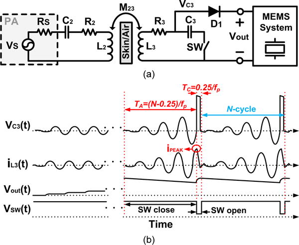
(a) Lumped model of the proposed multi-cycle resonance rectifier for inductively-powered MEMS system and (b) its switching waveforms
Fig. 2 shows the MCRR equivalent circuits for the accumulation (Fig. 2a), onset of charging (Fig. 2b), and the rest of charging (Fig. 2c) periods. The simplified circuit for the accumulation period is shown in Fig. 3, divided into Tx and Rx equivalent circuits. To simplify the circuit analysis, we have assumed that during TC, all the stored energy in L3C3-tank is transferred to RL and the remaining energy in the L3C3-tank after charging periods is zero, which means the initial condition for iL3(0) = 0 A. This is a reasonable assumption because during TC, iL3(t) drops much faster than typical LC-tank oscillation. Thus, D1 is turned off when iL3(t) drops very close to zero at the end of the charging period. Since TC ≪ TA, the effect of load resistance, RL, on the reflected impedance onto the Tx side, ZREF is negligible [10]. Therefore, ZREF can be derived from,
| (1) |
where RSW is the on resistance of the SW switch, M23 is the mutual coupling between Tx and Rx coils, and R3 is the parasitic resistance of L3. The reflected voltage, V32, across L3 in the steady-state condition can be calculated from,
| (2) |
where R2 is the parasitic resistance of L2. Therefore, the steadystate current in the Rx loop, iL3(t), can be derived from,
| (3) |
Considering that both L2C2 and L3C3 tanks are tuned at fp, the solution for (3) in Fig. 2a can be derived as,
| (4) |
At the end of TA, t = (N−0.25)/fp, current in L3 reaches its peak value, iPEAK, as shown in Fig. 1b, which can be found from (3),
| (5) |
where N = TA ×fp+0.25 is number of cycles in the accumulation period to be decided by the optimization procedure. At this time, SW opens and the charging period begins, as shown in Fig. 2b. Since one terminal of C3 opens at the charging period, C3 does not resonate with L3. Since iL3 cannot change abruptly, it decreases linearly, proportional to the voltage across L3, while turning on D1 and charging CL, as long as iL3 > 0 A. The capacitor voltage, VC3, also increases until VC3 = VD + Vout, where VD is the voltage drop across D1, and iL3(t) during the charging phase follows this linear equation,
| (6) |
When iL3,ch(t) crosses zero, the charging stops automatically due to D1 turning off. Hence, the charging time can be found from,
| (7) |
where VD is the voltage drop across D1. Since in typical application Vout ≫ VD, we can assume Vout + VD ≈ Vout. As shown in (7), charging time is inversely proportional to Vout. Therefore, the lowest Vout requires the longest charging time. In MCRR, the minimum Vout happens when Vout is less then steady state amplitude of VC3. When Vout is lower than VC3,Peak, D1 in Fig. 1a is turned on regardless of SW status, resulting in Vout,min = VC3,Peak. Since we are assuming that L3C3-tank is resonating, VC3,Peak = v(L/C) × iPEAK. Accordingly, tch,max = T/2π, which is less than the charging period (TC), chosen as a quarter cycle.
Fig. 2.

Equivalent circuits of various MCRR periods in a 2-coil inductive link, (a) accumulation period, (b) the onset of charging period, and (c) the rest of charging period.
Fig. 3.

Simplified equivalent circuit for accumulation period, seen from the Tx side at resonance. The Rx side is also considered because of its effect on the transient mode calculations.
The stored energy in L3 at the beginning of the charging period is,
| (8) |
while the energy loss due to the parasitic resistance of L3 and D1 during TC can be calculated as,
| (9) |
where RD1 is the ON-resistance of D1. Since the load capacitor, CL, is often selected large enough to minimize the ripple across the load resistance, RL, output voltage variations, ΔVout, during one cycle of TA + TC can be ignored in comparison with the rectifier output voltage, Vout. With this assumption, the energy delivered to RL in N carrier cycles can be derived as,
| (10) |
To turn on D1, VC3 should reach Vout+iPEAKRD1, and iL3 should charge the parasitic capacitances of D1 and SW, which are represented by CPD and CPM, respectively. When SW opens, CPM is connected in series with C3, and because C3 is much larger than CPM, the total capacitance of the series C3-CPM is almost equal to CPM. The energy needed for charging CPD and CPM can be found from,
| (11) |
where CP = CPD + CPM. As shown in Fig. 1b, VC3 is remained at Vout, and it drops when SW is closed. Therefore, ECP is dissipated through SW. At the steady state, the stored energy, EL3, should be equal to the sum of ELoad, Eloss, and ECP,
| (12) |
| (13) |
Therefore,
| (14) |
and Vout can be calculated by solving (14). Consequently, PLoad = PDL can be found from .
III. Design and Optimization of the MCRR
A. Diode and switch specs
As we mentioned in section II, parasitic capacitors of the diode and switch should be charged (ECP) before charging of CL, and (11) shows how much energy is dissipated when charging them. Typically, minimizing the diode or switch parasitic capacitance to reduce ECP means using smaller device size. However, this can result in increased Eloss due to higher turn-on voltage and parasitic on-resistance for D1 and SW, respectively. In addition, the higher on-resistance of SW, reduces EL3 following (5) and (8). Thus, the diode and switch specs should be carefully selected considering the trade-offs between Eloss and ECP, as well as the carrier frequency, fp. Since the prototype MCRR in this article is designed to provide a high output voltage, Vout, in a low power application, such as electrostatic MEMS sensors and actuators, ELoad is small and can be dominated by ECP from (11). Accordingly, the system does not require a very high iPEAK, which leads to small Eloss, in a way that it can be dwarfed by ECP. Therefore, we can conclude that a small-sized switch and diode with minimum CP are more beneficial for this MCRR prototype. BAT42 (Vishay, CT) and DMN5L06K (Diodes Inc., Tx), which have relatively higher turn-on resistance and smaller parasitic capacitance, were chosen as D1 and SW, respectively in the discrete MCRR prototype.
In an integrated circuit (IC) implementation, there are two choices for implementing D1; a passive Schottky diode or an active diode [18]. The conduction time of D1 is much smaller than 1/fp, which indicates a need for rapid on/off operation of the active diode. If the active diode turns on slowly, the parasitic capacitance of D1 and SW will be charged higher than Vout, and further increase ECP. When the active diode turns off slowly, iL3 will discharge CL when it changes its direction. Therefore, strong driver circuitry for the active diode becomes an issue, considering its additional power consumption for fast operation.
B. Number of resonant cycles
ECP and EL3 should be considered when finding the optimal number of carrier cycles, N, that would provide the highest PDL, and consequently the highest Vout, in the proposed MCRR. As shown in Fig. 4a, the stored energy in L3 increases according to (5) and (8) in a nonlinear fashion with respect to TA. Fig. 4b shows the same variables in Fig. 4a, which are divided by the elapsed time, represented by the number of cycles up to that point, to show the delivered and dissipated power levels in the MCRR. If the energy accumulation period, TA, is too short, not only the stored energy in L3 would not be enough but also most of the harvested energy will be spent on charging the parasitic capacitors, CPD and CPM, resulting in low PDL. On the other hand, if TA is too long, stored energy in L3C3-tank is saturated, and leads to reduction in PDL for longer periods of TA + TC. Therefore, optimization of N is critical for the proposed MCRR technique, and it can be found in Fig. 4a at the point where ELoad overcomes ECP, or in Fig. 4b where PLoad reaches its peak. One can also derive Vout from (14) and differentiate it with respect to N to find its optimal value mathematically, which is highlighted in Fig. 4 by a vertical red line.
Fig. 4.
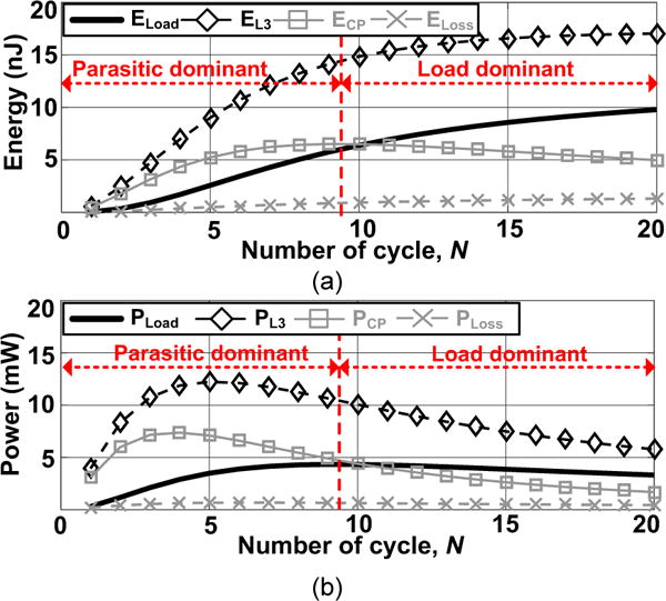
(a) Various stored or dissipated energies in the MCRR: EL3, ELoad, Eloss, and ECP vs. the number of resonance cycles, N. (b) Delivered and dissipated powers in the MCRR: PL3, PLoad, Ploss, and PCP vs. N. The optimal number of cycles, highlighted by a vetical red line, is determined by the peak of PLoad.
Although the proposed MCRR in this paper is focused on the PDL optimization, the maximum PTE is also acquired by the PDL optimization procedure when the weak coil coupling [8]. As discussed in MCRR analysis, the variation of the reflected load (ZREF) is negligible relative to N when N has a large number. Accordingly, the input power is independent on N in this situation, and achieving the maximum PDL means the maximum PTE in the proposed MCRR.
C. Inductive link optimization
According to (14), in addition to N, the Tx and Rx coil specifications clearly affect Vout. Therefore, the inductive link can be optimized specifically based on the aforementioned MCRR operating principles to further improve the PDL. The Tx and Rx coils in this paper are considered printed spiral coil (PSC) with rounded square shape because it has 1.1 times larger mutual inductance with the same diameter [26]. Self-inductance of the rounded square shape PSC can be calculation from [29],
| (15) |
| (16) |
where Do and Di are the outer and inner diameters of the coil. To calculate parasitic resistance of the PSC,
| (17) |
| (18) |
| (19) |
where lc is length, ρ is resistivity, tc is thickness, w is width, s is spacing of the conductive line, δ is the skin depth μr is the relative permeability, and μ0 is the permeability of space [26]. The mutual inductance, M, between two single-turn Tx and Rx coils can be found from,
| (20) |
where D is coils relative distance, and K and E are the complete elliptic integrals of 1st and 2nd kind [26]. Total mutual inductance between Tx and Rx coils can be calculated by adding every pair of single turns in the Tx and Rx coil,
| (21) |
where g is a coefficient dependent on the shape. For rounded square shaped coils, g = 1.21 [26].
To optimize the coils for MCRR, an iterative design procedure is proposed in Fig. 5 with the purpose of achieving the target output voltage (VTarget) with the highest possible PDL when RL is given. The source voltage (VS) on the Tx side is also given an initial value and the proposed procedure finds the optimal Tx and Rx coil geometries and the N, which can achieve VTarget with the lowest possible VS. Once VS(min) for VTarget is determined, increasing VS further obviously yields higher Vout and PDL, if those are desired. With respect to coil design, in most WPT applications, particularly the wirelessly-powered implantable medical devices (IMD), the Rx side is heavily size-constrained, resulting in limitation of the outer diameter of the Rx coil (DORx). Hence, the other coil geometrical parameters, such as the outer diameter of Tx coil (DOTx), and inner diameters of Tx (DiTx) and Rx coils (DiRx) can be optimized accordingly. The number of turns for Tx and Rx coils, nTx and nRx, are calculated considering these parameters and the optimal width of the conductive traces of the Tx and Rx coils, DwR and DwT, respectively. Based on the coil specifications in each outer loop iteration, there is an inner loop that finds the optimal N and Vout(max) for RL based on (14). By comparing Vout(max) and VTarget, the algorithm eventually finds the optimal geometries of the Tx and Rx coils along with their associated optimal N. The initial values; DiTx,init, DiRx,init, DOTx,init, DwT,init, and DwR,init are determined by the fabrication limits, such as minimum design rules for PSC lithography and fabrication, and the boundaries; DwR,lim, DwT,lim, DwT,lim, DwR,lim and DOT,lim are empirically determined to include the optimal point.
Fig. 5.

Optimization flowchart for the MCRR. DwR,init, DwT,init, DiRx,init, DiTx,init, and DOTx,init are initial value of DwR, DwT, DiRx, DiTx, and DOTx, respectively. DwR,lim, DwT,lim, and DOTx,lim are the upper boundaries of Rx and Tx PSC line width, and Tx outer diameter, respectively.
D. MCRR-Based optimization example
Here we demonstrate an example MCRR-based optimization procedure for a target application in wirelessly powering small ultrasound transducers that can perform ultrasound imaging from inside the body [30]. Based on other electrostatic MEMS sensor specifications, we have targeted PDL of 4 mW at VTarget = 20 V, which are the equivalent of RL = 100 kΩ, with 1.3 cm nominal Tx-Rx coil separation [14], at fp = 6.78 MHz, in the industrial-scientific-medical (ISM) band. Running the optimization procedure in Fig. 5 with a set of design constraints and initial values that are summarized in the upper half of Table I, yields the optimized MCRR specifications that are listed in the lower half of that table. Fig. 6a shows how the Tx coil was optimized at DoTx = 8 cm with a line width of 3.4 mm to achieve Vout = 20.6 V and PDL = 4.24 mW.
TABLE I.
Prototype MCRR Design Constraints and Specifications
| Design Constraints | |||
|---|---|---|---|
| Outer diameter of Rx coil (DoRx) | 1 cm | ||
| L2-L3 nominal distance (d23) | 1.3 cm | ||
| Target load (RL) | 100 kΩ | ||
| Target output voltage (VTarget) | 20 V | ||
| PDL | 4 mW | ||
| Switch Resistance (RSW) | 2 Ω | ||
| PA output resistance (RS) | 3.5 Ω | ||
| Carrier frequency (fp) | 6.78 MHz | ||
| Source voltage (VS) | 1.8 V | ||
| Initial value of DwR and DwT | 0.15 mm | ||
| Initial value of DiRx and DiTx | 1 mm | ||
| Initial value of DOTx | 5 mm | ||
| Optimized Rounded Square PSC Specifications | |||
| Rx (L3) | Tx (L2) MCRR | Tx (L2) CHWR | |
| Inductance, L (μH) | 1.17 | 3.49 | 1.91 |
| Parasitic res, R (Ω) | 2.3 | 2.02 | 1 |
| Outer diameter, DO (cm) | 1 | 8 | 8 |
| Inner diameter, Di (mm) | 2 | 1.1 | 0.5 |
| Line width, Dw (mm) | 0.15 | 3.35 | 4.7 |
| Line spacing, S (mm) | 0.15 | 0.3 | 0.33 |
| Thickness, T (μm) | 35 | 14 | 14 |
| Number of turns, n | 13 | 9 | 7 |
| Quality factor, Q | 21.6 | 73.6 | 81.36 |
| Mutual inductance (nH) | – | 68.02 | 51.58 |
Fig. 6.

(a) MCRR output voltage vs. outer diameter and conductive trace width of the Tx rounded square PSC from optimization process. N and inner diameter of Tx/Rx coils were optimized for each point, VS = 1.8 V, and RL = 100 kΩ. Max (Vout, PDL) = (20.6 V, 4.24 mW). (b) An ideal half-wave rectifier output voltage with Tx-Rx PSCs that are optimized in a conventional fashion as in [28] with the same VS and RL. Max (Vout, PDL) = (13.6 V, 1.8 mW).
For the sake of comparison, we have run the conventional PSC optimization algorithm in [28] for a 2-coil inductive link, followed by a conventional half-wave rectifier (CHWR) in Fig. 7, consisting of the same Schottky diode, D1, that was used in the MCRR with turn-on voltage of VD. The PDL was calculated in the same conditions as the MCRR (VS = 1.8 V, and RL = 100-kΩ) [28],
| (22) |
where Q2 and Q3 are quality factors of Tx and Rx PSCs, respectively, and Q3L is the loaded quality factor of Rx. Considering the equivalent loading through the rectifier [31],
| (23) |
where V2 is the peak voltage across C3. Consequently, Q3L is calculated from [28],
| (24) |
where ωp = 2πfp. The output voltage can be calculated from the PDL in (22),
| (25) |
Fig. 7.

Schematic diagram of a conventional half-wave rectifier (CHWR) with parallel LC-tank on the Rx side, which is more suitable for large RL.
Fig. 6b shows that the output voltage in this case reaches a maximum of 13.6 V with PDL = 1.8 mW, which is far lower than that of the MCRR. It should also be noted that, as reflected in Table I, the PSCs optimized through the conventional WPT method have the same geometry on the Rx side, but different geometries on the Tx side compared to the PSCs optimized for the MCRR through Fig. 5 algorithm.
Once optimized geometries of the Tx-Rx coils are found, they are used in Fig. 8 to give further insight on how Vout varies in MCRR with respect to the changes in coil separation (d23), optimal N, and RL. As mentioned in Section III.C, N is mostly a function of the ratio between PDL and power dissipated in coils, diode, and switch parasitics. Therefore, the white curve in Fig. 8a, which indicate optimal N at every d23, shows that changing the coils’ distance does not change N. On the other hand, when the load is changed from 1 kΩ to 1 MΩ in Fig. 8b, the optimal N varies significantly, from 5 cycles to 16 cycles.
Fig. 8.

Output voltage variations in the MCRR vs. (a) N and coil separation, d23. (b) N and RL. The white curves over these 3D surfaces show the optimal N.
IV. Simulation and Measurement Results
Tx and Rx PSCs were fabricated on 0.5 oz. and 1 oz. PSCs, respectively, following the optimized geometries in Table I. The MCRR prototype in Fig. 9 consists of BAT42 (Vishay, Malvern, PA) as D1 and DMN5L06K (Diodes Inc., Plano, TX) as a SW in Fig. 1a, driven by a function generator (AFG3102, Tektronix). We also used the same function generator for VS to provide a precise constant voltage for the carrier signal regardless of the Tx coil input resistance, with an emulated source resistance of RS = 3.5 Ω. The Tx-Rx coils were held in parallel at d23 = 1.3 cm, using insulating materials. Fig. 8b shows measured waveforms from key nodes (VC3, VSW, and Vout) in Fig. 1a circuit when the MCRR operates at 6.78 MHz. In this case, at N = 10, SW is closed for 9¾ cycles (VSW is high), during which period oscillating amplitude of VC3 increases up to 6.8 V.
Fig. 9.

(a) Discrete MCRR prototype and experimental setup. (b) Measured waveforms from key nodes of the MCRR circuit in Fig. 1.
Then, SW is opened for ¼ cycles, and VC3 is boosted up to 25 V because of rapid drop in iL3 and VL3 = L3(diL3/dt). Fig. 10 compares calculation, simulation, and measurement of Vout vs. N using (14), Fig. 1a simulation in Cadence, and measurements on MCRR prototype in Fig. 9 and Tx-Rx coils in Table I, respectively. We achieved rectified output voltage of 20.9 V across the 100 kΩ load when d23 = 1.3 cm. In Fig. 10, at low N, calculation has a small difference with measurement because of the nonlinearity of parasitic capacitances of D1 and SW, which depend on the voltage across them, and have not been considered in our model. Since at low N, the energy loss, ECP, is dominant and proportional to these parasitic capacitors, this difference is more obvious than at higher N values. In Fig. 11a, the measured and calculated output voltages in the MCRR is compared with the CHWR while changing the distance between their respective optimized coils, when VS and RL are the same. Even though the coils are optimized for the nominal d23 = 1.3 cm, it is clear that MCRR maintains its superiority over the conventional WPT link by boosting Vout up to 65.2% across this range. The MCRR curve also shows that the optimal N does not change with distance, in agreement with the white curve in Fig. 8a.
Fig. 10.

Output voltage vs. N. The results were calculated based on (14), simulated in Cadence, and measured using the setup in Fig. 8a.
Fig. 11.

Output voltage of MCRR and CHWR vs. (a) d23 when RL = 100 kΩ, and (b) RL when d23 = 1.3 cm. N is the optimal number of cycles to accumulate energy in the MCRR. (c) Comparing PDL vs. N in the MCRR and CHWR at RL = 5 kΩ, 12 kΩ, and 100 kΩ. (d) Comparing PDL vs. RL at RS = 1 Ω, 3.5 Ω, and 10 Ω. d23 = 1.3 cm.
Fig. 11b compares the MCRR and CHWR in terms of Vout at the nominal coil distance, when RL is changed over two orders of magnitude. In this case, MCRR generates higher Vout and consequently delivers more power to the load than CHWR for lighter loads, which means RL > 12 kΩ in this prototype. For heavier loading, i.e. lower RL, which according to Fig. 8b correspond to smaller optimal N, however, CHWR provides higher Vout and PDL. In order to explain this observation, in Fig. 11c we have compared the PDL in MCRR and CHWR for RL = 5 kΩ (heavy), 12 kΩ (moderate), and 100 kΩ (light) loading vs. N. It can be seen that by decreasing RL, PDL(max) in both MCRR and CHWR increase. However, the increment in the CHWR is considerably faster than MCRR. The PDL in CHWR is independent of N because in this WPT mechanism, the L3C3-tank maintains its induced voltage amplitude and a small but steady amount of power (energy) is delivered to the load in each carrier cycle. MCRR, however, builds up the induced voltage by accumulating energy in the L3C3-tank over TA and suddenly delivering it to the load during TC. Thus it is very much dependent on N, as shown in Fig. 10.
Because of this fundamental difference in operation, CHWR is always loaded by RLeq in (23) and operates under Q3L in (24) on the Rx side, which are heavily dependent on RL and reflect onto the Tx side as ZREF in Fig. 3 [31]. For large RL, Vout is large, and CHWR is at a disadvantage because Q3L/QL is low, and ZREF > R2 + RS on the Tx side, resulting in poor impedance matching and low PDL. On the other hand, according to (1), ZREF in the MCRR is almost independent of RL, and instead heavily depends on RSW and R3. Moreover, unlike CHWR, MCRR is capable of maximizing PDL and Vout by adjusting N, as an additional degree of freedom. For small RL, Vout and RLeq are low, and Q3L in CHWR is considerably higher, resulting in ZREF that is much closer to R2 + RS, thus improving the impedance matching on the Tx side and increasing PDL. The MCRR, however, suffers from the additional RSW in the L3C3 resonance loop, and has only modest increment in the PDL due to reduced ECP on the Rx side, according to Fig. 11c and (11).
To demonstrate the effect of impedance matching on the Tx side, we have changed the source output resistance in Fig. 11d, which compares PDL in MCRR and CHWR vs. RL at RS = 1 Ω, 3.5 Ω, and 10 Ω. It can be seen that for MCRR, the RL which generates PDL(max) does not change with RS, supporting the notion that in MCRR, ZREF is almost independent of RL. In CHWR, however, increasing RS moves the peak of PDL towards higher RL. Since in both MCRR and CHWR less power dissipation in RS means increased PDL, when these two effects are considered together, increasing RS shifts the crossing point, at which PDL(MCRR) = PDL(CHWR) to lower RL.
It is worth noting that at very low RL < 1 kΩ, because, as discussed in Chapter II, when Vout < VC3,Peak, D1 is turned on regardless of SW status the resulting in significantly reduced energy accumulation in L3C3 (EL3). As a result, the MCRR operating mechanism falls apart, and the abovementioned circuit model in Fig. 2 and associated equations are no longer valid.
In Fig. 12 we have compared MCRR and CHWR in terms the overall efficiency (efficiency from the source voltage to output, η), which follows a similar trend as the PDL and Vout in Fig. 10. As shown in Fig. 12a, at the nominal conditions of VS = 1.8V, RL = 100 kΩ, and d23 = 1.3 cm, the MCRR achieves η = 2.2%, which is about 3 times larger than that of the CHWR at η = 0.75%. It can be seen that unlike [24] and [25], which consider the applicability of a mechanism like MCRR only in loosely coupled coils, the MCRR maintains its advantage over CHWR in a wide range of coil separations, i.e. various coupling coefficients, and the η improvement, in fact, grows with stronger coupling between the coils. Fig. 12b compares the MCRR and CHWR in terms of PTE at the nominal coil distance, when RL is changed over two orders of magnitude. These graphs, similar to Fig. 11b, show the true areas of MCRR superiority where RL is large and high Vout is needed, depending on the WPT application, and 2-coil CHWR fails to create the optimal matching conditions on the Tx or Rx side. One should, however, note that the multi-coil inductive links [28] and multi-cycle Q-modulation technique [10] are also capable of creating optimal matching conditions, and should be considered depending on WPT circuit parameters and the application.
Fig. 12.

Overall efficiency of MCRR and CHWR vs. (a) d23 when RL = 100 kΩ, and (b) RL when d23 = 1.3 cm. N is the optimal number of cycles in the MCRR.
Calculation and measurement of the optimal N may show ±1 cycle discrepancy, as can be seen in Figs. 11 and 12. This can be explained by the non-linearity of the parasitic capacitance of the switch and diode, which are not considered in calculations as mentioned earlier. Although the capacitance variation is not large, Vout variations around the optimal N is also very small, as can be seen in Fig. 10. Therefore, the output voltage at the calculated optimal N is almost the same as the maximum measured voltage despite this discrepancy.
In the MCRR, we assume charging time is well controlled, and we can open the switch at the exact point when iL3 is at its peak, θ = 3/2π. Since the MCRR uses L3 as a current source over TC, and the amount of current is determined by iL3 at the beginning of TC, the output of the MCRR is heavily dependent on when the TC starts. In Fig. 13, we have shown the MCRR output with phase error, Δθ, which is the phase difference between the starting point of TC and optimal θ = 3/2π. Since the MCRR opens SW for a quarter cycle, the output decreases for |Δθ| < 90°. For |Δθ| > 90°, although we open the SW, the direction of iL3 is against the direction of the D1, and load is not charged during TC. On the other hand, during TA, the MCRR works like the CHWR with decreased Q (because of RSW), and load is charged during TA. Therefore, the output voltage of the MCRR is constant when |Δθ| > 90°.
Fig. 13.

Output of the MCRR v.s. phase error (Δθ) when d23 = 1.3 cm, RL = 100 kΩ, and N=9.
V. Conclusions
We have presented detailed optimization procedure for the multi-cycle resonance rectifier (MCRR), which can achieve considerably higher PDL and efficiency, while boosting the output voltage in wireless powering of high voltage, low power applications, such as electrostatic MEMS sensors compared to conventional methods. The MCRR can be easily implemented with a diode, a switch, and a fast control signal that is synchronized with the power carrier. The MCRR harvests energy from the resonant magnetic field and accumulates it in a series Rx L3C3-tank over a certain number of carrier cycles, then suddenly opens the switch at the peak of the coil current to transfer that energy to the load through the diode in a quarter of a carrier period. Key parameters and the design guideline for optimizing the MCRR components, number of cycles for accumulating energy, and specific coil geometries are provided with governing equations. Through an example WPT link, we have compared various aspects of the MCRR operation against that of a conventional half-wave rectifier (CHWR) and clearly identified their pros and cons, and where one method might be preferred over the other. Measurement results have verified the derived equations for calculating the desired output voltage and the optimal N.
Acknowledgments
The project described was supported by Award Number R21 EB017365-02 from the National Institute of Biomedical Imaging and Bioengineering (NIBIB). The content is solely the responsibility of the authors and does not necessarily represent the official views of the NIBIB or the National Institutes of Health (NIH).
Biographies

Jaemyung Lim (S’13) earned a bachelor’s degree in electrical and computer engineering from Hanyang University in Seoul and a master’s degree in electrical and computer engineering from Georgia Tech. He is currently working on his doctoral degree in electrical and computer engineering, conducting research on developing an wireless read-out system-on-a-chip for intravascular ultrasound imaging with capacitive micromachined ultrasonic transducers (CMUTs). His research interests include MEMS interface IC, analog and mixed circuit design, wireless data communication, power management IC, and wireless power transmission.

Byunghun Lee (S’11) received the B.S. degree from Korea University, Seoul, South Korea, and the M.S. degree from Korea Advanced Institute of Technology (KAIST), Daejeon, South Korea, in 2008 and 2010, respectively.
From 2010 to 2011, he worked on wireless power transfer systems at KAIST as a design engineer. He received his Ph.D. degree in Electrical and Computer Engineering at Georgia Institute of Technology. His research interests include analog/mixed-signal IC design and wireless power/data transfer systems for biomedical applications.

Maysam Ghovanloo S’00–M’04–SM’10) received the B.S. degree in electrical engineering from the University of Tehran, Tehran, Iran, in 1994, the M.S. degree in biomedical engineering from the Amirkabir University of Technology, Tehran, Iran, in 1997, and the M.S. and Ph.D. degrees in electrical engineering from the University of Michigan, Ann Arbor, in 2003 and 2004, respectively. From 2004 to 2007, he was an Assistant Professor at the Department of Electrical and Computer Engineering, NC-State University, Raleigh, NC. He joined the faculty of Georgia Institute of Technology, Atlanta, GA in 2007 where he is currently an Associate Professor and the Founding Director of the GT-Bionics Lab in the School of Electrical and Computer Engineering. He has authored or coauthored more than 200 peer-reviewed publications.
Dr. Ghovanloo was the general chair of the IEEE Biomedical Circuits and Systems (BioCAS 2015) in Atlanta, GA. He is an Associate Editor of the IEEE Transactions on Biomedical Engineering and IEEE Transactions on Biomedical Circuits and Systems. He served as an Associate Editor of IEEE Transactions on Circuits and Systems, Part II (2008–2011), as well as a Guest Editor for the IEEE Journal of Solid-State Circuits and IEEE Transactions on Neural Systems and Rehabilitation Engineering. He has also served on the Imagers, MEMS, Medical and Displays subcommittee of the International Solid-State Circuits Conference (ISSCC) from 2009–2014. He has received the National Science Foundation CAREER Award, the Tommy Nobis Barrier Breaker Award for Innovation, and Distinguished Young Scholar Award from the Association of Professors and Scholars of Iranian Heritage.
References
- 1.Finkenzeller K. RFID-Handbook. 2nd. Hoboken, NJ: Wiley; 2003. [Google Scholar]
- 2.Chwei-Sen Wang, Stielau Oskar H, Covic Grant A. Design considerations for a contactless electric vehicle battery charger. IEEE Trans Ind Electron. 2005 Oct;52(5):1308–1314. [Google Scholar]
- 3.Covic GA, Boys JT, Kissin MLG, Lu HG. A three-phase inductive power transfer system for roadway-powered vehicles. IEEE Trans Ind Electron. 2007 Dec;54(6):3370–3377. [Google Scholar]
- 4.Kissin MLG, Boys JT, Covic GA. Interphase mutual inductance in polyphase inductive power transfer systems. IEEE Trans Ind Electron. 2009 Jul;56(7):2393–2400. [Google Scholar]
- 5.Kiani M, Jow U, Ghovanloo M. Design and optimization of a 3-coil inductive link for efficient wireless power transmission. IEEE Trans Biomed Circuits Syst. 2011 Dec;5(6):579–591. doi: 10.1109/TBCAS.2011.2158431. [DOI] [PMC free article] [PubMed] [Google Scholar]
- 6.Lee B, Kiani M, Ghovanloo M. A triple-loop inductive power transmission system for biomedical applications. IEEE Trans Biomed Circuits Syst. 2015 Feb;10(1):138–148. doi: 10.1109/TBCAS.2014.2376965. [DOI] [PubMed] [Google Scholar]
- 7.Li X, Tsui C, Ki W. A 13.56 MHz wireless power transfer system with reconfigurable resonant regulating rectifier and wireless power control for implantable medical devices. IEEE J of Solid-State Circuits. 2015 Apr;50(4):978–989. [Google Scholar]
- 8.Choi JH, Yeo SK, Park S, Lee JS, Cho GH. A resonant regulating rectifier (3R) operating at 6.78 MHz for a 6 W wireless charger with 86% efficiency. IEEE J of Solid-State Circuits. 2013 Dec;48(12):2989–3001. [Google Scholar]
- 9.Kiani M, Lee B, Yeon P, Ghovanloo M. A Q-modulation technique for efficient inductive power transmission. IEEE J of Solid-State Circuits. 2015 Dec;50(12):2839–2848. doi: 10.1109/JSSC.2015.2453201. [DOI] [PMC free article] [PubMed] [Google Scholar]
- 10.Lee B, Yeon P, Ghovanloo M. A multi-cycle Q-modulation for dynamic optimization of inductive links. IEEE Trans Industrial Electronics. 2016 Apr;63(8):5091–5100. doi: 10.1109/TIE.2016.2550009. [DOI] [PMC free article] [PubMed] [Google Scholar]
- 11.Chitnis G, Maleki T, Samuels B, Cantor LB, Ziaie B. A minimally invasive implantable wireless pressure sensor for continuous IOP monitoring. IEEE Trans Biomed Circuits Syst. 2013 Jan;60(1):250–256. doi: 10.1109/TBME.2012.2205248. [DOI] [PubMed] [Google Scholar]
- 12.Lim J, Tekes C, Degertekin FL, Ghovanloo M. Towards a reduced-wire interface for CMUT-based intravascular ultrasound imaging systems. IEEE Trans Biomed Circuits Syst. 2017 Apr;11(2):400–410. doi: 10.1109/TBCAS.2016.2592525. [DOI] [PMC free article] [PubMed] [Google Scholar]
- 13.Serrano DE, Zaman MF, Rahafrooz A, Hrudey P, Lipka R, Younkin D, Nagpal S, Jafri I, Ayazi F. Substrate-decoupled, bulk-acoustic wave gyroscopes: Design and evaluation of next-generation environmentally robust devices. Microsystems & Nanoengineering. 2016 Apr; doi: 10.1038/micronano.2016.15. [DOI] [PMC free article] [PubMed] [Google Scholar]
- 14.Gurun G, Tekes C, Zahorian J, Xu T, Satir S, Karaman M, Hasler J, Degertekin FL. Single-Chip CMUT-on-CMOS Front-End System for Real-Time Volumetric IVUS and ICE Imaging. IEEE Trans Ultrason Ferroelectr Freq Contl. 2014 Feb;61(2):239–250. doi: 10.1109/TUFFC.2014.6722610. [DOI] [PMC free article] [PubMed] [Google Scholar]
- 15.IEEE Standard for Safety Levels With Respect to Human Exposure to Radio Frequency Electromagnetic Fields, 3 kHz to 300 GHz. IEEE Std. 2005;C95.1:1. [Google Scholar]
- 16.Gabriel S, Lau RW, Gabriel C. The dielectric properties of biological tissues: II. Measurements in the frequency range of 10 Hz to 20 GHz. Phys Med Biol. 1996;41:2251–2269. doi: 10.1088/0031-9155/41/11/002. [DOI] [PubMed] [Google Scholar]
- 17.Qu X, Jing Y, Han H, Wong S, Tse C. Higher order compensation for inductive-power-transfer converters with constant-voltage or constant current output combating transformer parameter constraints. IEEE Trans Power Electron. 2016 to be published. [Google Scholar]
- 18.Lee H, Ghovanloo M. A high frequency active voltage doubler in standard CMOS using offset-controlled comparators for inductive power transmission. IEEE Trans Biomed Circuits Syst. 2013 Jun;7:213–224. doi: 10.1109/TBCAS.2012.2198649. [DOI] [PMC free article] [PubMed] [Google Scholar]
- 19.Choi JH, Park SK, Lee JS, Choi GH. Resonant regulating rectifier (3R) operating for 6.78 MHz resonant wireless power transfer (RWPT) IEEE J of Solid-State Circuits. 2016 Nov;48(12):2989–3001. [Google Scholar]
- 20.Hameed Z, Moez K. Hybrid forward and backward threshold compensated RF-DC power converter for RF energy harvesting. IEEE J Emerg Sel Topics Circuits Syst. 2014 Sep;4:335–343. [Google Scholar]
- 21.Singh B, Singh BN, Chandra A, Al-Haddad K, Pandey A, Kothari D. A review of single-phase improved power quality AC-DC converters. IEEE Trans Industrial Electronics. 2003 Oct;50:962–981. [Google Scholar]
- 22.Palumbo G, Pappalardo D. Charge pump circuits: an overview on design strategies and topologies. IEEE Circuits Syst Mag. 2010;10:31–45. [Google Scholar]
- 23.Tang H, Seo D, Singhal U, Li X, Maharbiz MM, Alon E, Boser BE. Miniaturizing ultrasonic system for portable health care and fitness. IEEE Trans Biomed Circuits Syst. 2015 Dec;9(6):767–776. doi: 10.1109/TBCAS.2015.2508439. [DOI] [PubMed] [Google Scholar]
- 24.Gougheri HS, Kiani M. Current-based resonant power delivery with multi-cycle switching for extended-range inductive power transmission. IEEE Trans Circuits Syst I, Reg Papers. 2016 Sep;63(9):1543–1552. [Google Scholar]
- 25.Choi M, Jeong T, Jeong S, Blaauw D, Sylvester D. A resonant current-mode wireless power receiver and battery charger with −32 dBm sensitivity for implantable systems. IEEE J of Solid-State Circuits, vol PP, issue 99, pp. 2016 Aug;:1–13. [Google Scholar]
- 26.Jow U, Ghovanloo M. Design and optimization of printed spiral coils for efficient transcutaneous inductive power transmission. IEEE Trans Biomed Circuits Syst. 2007 Sep;1(3):193–202. doi: 10.1109/TBCAS.2007.913130. [DOI] [PubMed] [Google Scholar]
- 27.Harrison R. Designing efficient inductive power links for implantable devices. IEEE International Symphosium on Circuits and Systems, May. 2007:2080–2083. [Google Scholar]
- 28.Kiani M, Ghovanloo M. A Figure-of-merit designing highperformance inductive power transmission links. IEEE Trans Industrial Electronics. 2013 Nov;60(11):5292–5305. doi: 10.1109/TIE.2012.2227914. [DOI] [PMC free article] [PubMed] [Google Scholar]
- 29.Wheeler HA. Formulas for the skin effect. Proc IRE. 1942 Sep;30(9):412–424. [Google Scholar]
- 30.Saijo Y, Van der Steen AFW. Vascular ultrasound. Tokyo, Japan: Springer; 2003. Part 2: The technical potential of IVUS; pp. 51–166. [Google Scholar]
- 31.Ghovanloo M, Atluri S. An integrated full-wave CMOS rectifier with built-in back telemetry for RFID and implantable biomedical applications. IEEE Trans Circuits Syst I, Reg Papers. 2008 Nov;55(10):3328–3334. [Google Scholar]