

Abstract
Biophysicists have long sought optical methods capable of reporting the electrophysiological dynamics of large-scale neural networks with millisecond-scale temporal resolution. Existing fluorescent sensors of cell membrane voltage can report action potentials in individual cultured neurons, but limitations in brightness and dynamic range of both synthetic organic and genetically encoded voltage sensors have prevented concurrent monitoring of spiking activity across large populations of individual neurons. Here we propose a novel, inorganic class of fluorescent voltage sensors: semiconductor nanoparticles, such as ultrabright quantum dots (qdots). Our calculations revealed that transmembrane electric fields characteristic of neuronal spiking (~10 mV/nm) modulate a qdot’s electronic structure and can induce ~5% changes in its fluorescence intensity and ~1 nm shifts in its emission wavelength, depending on the qdot’s size, composition, and dielectric environment. Moreover, tailored qdot sensors composed of two different materials can exhibit substantial (~30%) changes in fluorescence intensity during neuronal spiking. Using signal detection theory, we show that conventional qdots should be capable of reporting voltage dynamics with millisecond precision across several tens or more individual neurons over a range of optical and neurophysiological conditions. These results unveil promising avenues for imaging spiking dynamics in neural networks and merit in-depth experimental investigation.
Keywords: voltage-sensitive indicators, fluorescence microscopy, neurophysiology, quantum dots, semiconductor heterostructures
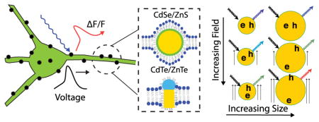
Graphical Abstract
Biophysicists and neuroscientists have long sought to understand how the interactions between individual neurons collectively yield network dynamics. To study such phenomena, biophysicists have worked for decades to develop optical reporters of neuronal membrane voltage, with the goal of concurrently visualizing neurons’ electrical dynamics and complex interactions.1 By comparison, multielectrode recording methods have already provided a wealth of data but have been restricted in their abilities to densely sample local microcircuits and to distinguish between neurons of different genetic classes.2
Optical sensors, in combination with suitable targeting strategies, have the potential to overcome both of these limitations. Indeed, in recent years, synthetic and genetically encoded fluorescent Ca2+ indicators have become prominent tools for imaging neural Ca2+ dynamics across large sets of individual neurons of known types.3–8 Nevertheless, though a useful correlation often exists between Ca2+ dynamics and neuronal spiking across a range of spike frequencies, the slowkinetics and saturation of [Ca2+]-related fluorescent signals constrain the utility of Ca2+ imaging as a means of probing spiking dynamics in many neuron types.4,9
Numerous voltage-sensitive indicators1,10–18 permit direct imaging of cellular membrane potentials. Organic voltage-sensitive dyes have allowed functional mapping studies in awake mammals14 and studies of individual cells’ dynamics in invertebrates19 and mammalian brain slices.20 However, such studies have often been constrained by the propensities of voltage-sensitive dyes toward photobleaching, phototoxicity, and nonspecific background labeling. Recently, several varieties of genetically encoded fluorescent voltage sensors have emerged that have allowed detection of aggregate neural activity in vivo and single spikes in vitro.11,15 These have been complemented by hybrid approaches that combine genetically encoded, membrane-targeted fluorescent proteins with synthetic voltage-sensing molecules.16 Nevertheless, these probes have been limited by slow kinetics and limited dynamic range,11 low quantum yields,15,21 and possible interference with cellular capacitance.16 These constraints have precluded concurrent detection of single action potentials across large populations of individual neurons in the live mammalian brain.
Toward addressing these challenges, we studied whether tools from nanotechnology, specifically, bright, multifunctional semiconductor quantum dots (qdots),22,23 might be useful for imaging neuronal membrane potentials. Qdots are known to possess voltage-sensitive optical properties, including a red-shifting of the qdot’s fluorescence emission peak, spectral broadening, and a decrease in the intensity of fluorescence emission (Figure 1C,D).24–27 Qdots also are highly resistant to photobleaching and exhibit large quantum yields and absorption cross sections for one- (σ1) and two-photon (σ2) excitation. For example, CdSe qdots with radius R ~ 3 nm exhibit cross sections of σ1 > 1 nm2 and σ2 > 3 × 10⁴ GM, as compared to σ1 ~ 10−2 nm2 and σ2 ~ 3 × 10² GM for green fluorescent protein.28,29
Figure 1.

Qdots exhibit a spectral red shift and decrease in fluorescence intensity in response to applied electric fields. Schematic drawings of a quantum dot embedded in a bilipid layer (A), where yellow indicates the dot core, green the exciton confining shell. (B) Qdot has been non-uniformly coated so that it is unscreened by the membrane. (C) Schematic indicating the field-induced exciton polarization and fluorescence red shift in qdots; ‘e’ and ‘h’ represent the electron and hole that are excited by the incoming light (black arrow). The pair recombine, producing fluorescence (colored arrows). (D) Schematic drawing of the modulation of a qdot’s absorption and emission spectra by an applied field (shifts exaggerated for clarity).
To evaluate the spike detection capabilities of qdot indicators quantitatively, we applied a theoretical approach that incorporates the physical, biophysical, and statistical components of the problem. We calculated the effect of applied electric fields on the qdot’s electronic structure and examined how this modulates a qdot’s fluorescence intensity and emission spectra. We also studied nonspherical, nonhomogenous qdots, which we refer to more generally as semiconductor nanocrystals, and found that these nanoparticles can demonstrate much greater voltage sensitivity than conventional qdots. This highlights the importance of rational design in the creation of nanoparticle sensors.
To quantify a qdot’s capabilities to detect action potentials, we modeled the roles of the qdot’s optical properties, the optical instrumentation, and neurophysiological parameters in setting the detection fidelity of voltage imaging experiments. We calculated how well the modulations of fluorescence lifetime and spectrum can enhance spike detection fidelity. We then examined neuronal spike detection using qdots in both wide-field epi-fluorescence and laser-scanning microscopy. We found that the voltage sensitivity and brightness of qdots should allow simultaneous monitoring of the spiking output of tens to possibly hundreds of cells. Thus, qdot and other nanoparticle voltage sensors merit in-depth experimental study.
RESULTS
Semiconductor Nanocrystals Have Voltage-Dependent Photophysical Properties
Absorption of a photon in a semiconductor nanocrystal excites a bound electron–hole pair, known as an exciton, which subsequently recombines by either radiative or nonradiative processes (Supporting Information). We modeled the dynamics of fluorescence excitation and emission in a nanocrystal as those of a two-state system, with rate constants ka for excitation of the pair, for radiative decay with fluorescence lifetime τr, and knr for nonradiative decay (Supporting Information). The lifetime is inversely proportional to the overlap between the electron and hole wave functions, τr ∝ |〈ψe|ψh〉| −2, and typically ranges between 10 and 100 ns, several times that of organic dyes and fluorescent proteins, which typically have lifetimes of ~1–10 ns.23
We found the wave functions for the electron and hole by treating them as distinct particles moving in a three-dimensional potential well and with different effective masses, and (Supporting Information). The particles’ energies are inversely proportional to their effective masses, which are intrinsic properties of the semiconductor. Although qdots can be synthesized from a number semiconductor materials, we restricted our attention to those made of type II–VI semiconductors, as these emit at visible and near-infrared wavelengths and represent the most photophysically robust type of qdot that is readily obtainable by present synthesis techniques.30 For II–VI semiconductors, , so holes have lower energy and are thus more susceptible to perturbations such as applied electric fields.
The fluorescence emission spectrum from a population of qdots at physiological temperatures exhibits a single peak at a wavelength that depends on the qdots’ size. Near this peak, the spectrum has an approximately Gaussian shape of ~30nm fwhm. This spectral width arises due to the inhomogeneous size distribution of the dots, thermal broadening, and Stark shifts caused by charge fluctuations on or near the dots’ surface that modulate their individual emission spectra (spectral diffusion).23,25
When a time-independent, spatially uniform electric field is applied to a qdot, the electron–hole pair polarizes along the field gradient, creating two optical signatures of applied fields: an increase in the qdot lifetime, τr, and a decrease in the emitted fluorescence energy, Eγ (Figure 1C,D). These shifts are electro-optic and occur on picosecond time scales, yielding nanocrystal response kinetics that are rapid compared to physiological time scales. Spherical qdots are often idealized as an infinite potential well. Upon application of a constant electric field, standard quantum mechanical perturbation theory yields scaling laws for the quantum-confined Stark shift, and the accompanying change in excited-state lifetime, (Supporting Information). Here, R is the qdot’s radius, and Ez is the strength of the electric field inside the qdot.
To compute a result more accurate than that from second-order perturbation theory, we used a nonperturbative finite matrix technique that can provide arbitrarily accurate approximations to the eigenstates of the Hamiltonian (Methods). Figure 2 displays voltage-dependent optical parameters for a range of qdot sizes, II–VI semiconductor materials, and field strengths, showing how the electrical polarizability scales with the qdot’s radius and the effective mass of the charge carrier. These calculations revealed that, without accounting for typical emission wavelengths, quantum yields, and absorption cross sections, materials with large effective hole masses, such as CdTe ( ), are more polarizable and hence show greater voltage sensitivity. For CdTe qdots of radius R = 4 nm, fractional lifetime changes of ~5% and shifts in the spectral mode of ~0.5 nm are achievable for electric fields Ez ~ 5 mV/nm, typical of transmembrane electric fields during neuronal action potentials (Figure 2).
Figure 2.
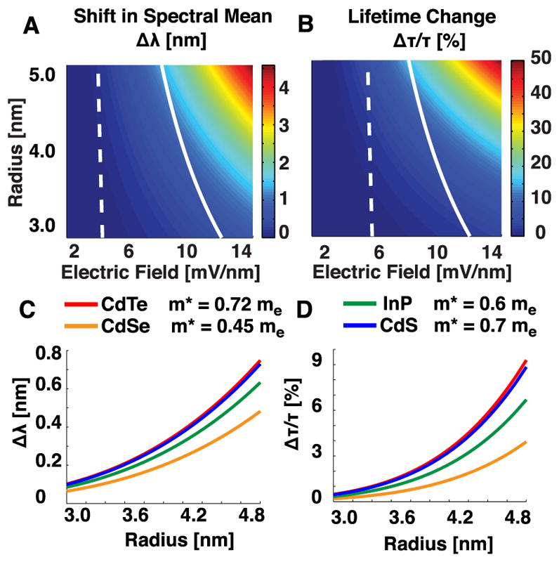
Sensitivity of qdots to electric fields depends on their size and material composition. (A) Relative wavelength shifts and (B) changes in the fluorescence radiative lifetime, as a function of radius and electric field for CdTe qdots. White curves indicate the field across a qdot due to a potential difference of V = −70 mV. The dashed line denotes a qdot screened by a 4 nm thick bilipid layer. The solid line indicates the field across an unscreened qdot. (C) Wavelength shifts and (D) fractional radiative lifetime changes for four common semiconductor materials32 as a function of radius, with a constant field E = 5 mV/nm across the dot.
The voltage-dependent change in fluorescence lifetime also produces a net change in fluorescence intensity. For example, in a two-state model in which a nanocrystal undergoes one-photon excitation at frequency ω and low intensity I, the total fluorescence is F = ΦFka, where ka = σ1/(ħω) is the rate constant for absorption, ΦF ≡ kr/(kr + knr) is the quantum yield, and σ1 is the one-photon cross section (Supporting Information). An increase in τr raises the fraction of excitation events that lead to nonradiative decay, which for small increases, Δτr, leads to linear reductions in fluorescence intensity (Supporting Information):
| (1) |
Neuronal Voltage Sensing with Membrane-Targeted Semiconductor Nanocrystals
We next examined the case of qdots embedded in a neural membrane, to assess their sensitivity to transmembrane voltages. Due to Debye screening, electric fields outside the cellular membrane decay exponentially with length constant of ~1 nm. A qdot placed completely within the membrane will therefore experience stronger electric fields and undergo greater modulation of its fluorescence properties. The electric field strength inside a qdot will depend on its composition, size, and shape and interaction with the lipid bilayer. The II–VI semiconductors discussed here have a static dielectric constant, εS ~ 10, much greater than that of the bilayer (εB ~ 2). Thus, qdots completely embedded in the membrane are subject to fields that are substantially screened (Supporting Information).
Although an exact treatment of the electric field in the membrane is beyond the scope of this paper, we considered two distinct simplified scenarios. In the first, the dot has a hydrophobic coating that targets it between the leaflets of the neural membrane. This has been achieved in bilipid layers but not yet in live neurons.31 In the second, the dot is localized to the membrane but not fully embedded inside of it; this scenario yields reduced electric screening in comparison to the first (Figure 1A,B). At transmembrane voltages of V = −70 mV, typical of neuronal resting potentials, the electric field across the membrane is Ez ~ 5 mV/nm (Figure 2A,B). For a CdTe qdot of 4 nm radius, this field yields an estimate of Δτr/τr ~ 2.5%.
Voltage Sensitivity of Type-II Semiconductor Nanoparticles
Recently developed chemical synthesis techniques have led to nanocrystals that separately limit the spatial extent of the electron and hole wave functions. These are known as type-II semiconductor nanoparticles, in analogy with structures synthesized by microfabrication techniques, and typically consist of a semiconductor nanorod grown on a quantum dot core.30 Because the tails of the individual carrier wave functions are more voltage-sensitive than the rest, a probe with electron–hole overlap confined to the tails of either wave function will show enhanced voltage sensitivity (Figure 3B).25,27 The asymmetry of the structure has an effect similar to electrically prebiasing the quantum dot, creating a fixed electric dipole moment that is more sensitive to small field shifts. This changes the dependence of the fluorescence shift on the applied field strength to a linear dependence, as opposed to the quadratic dependence for conventional qdots.
Figure 3.

Type-II semiconductor heterostructures exhibit greater voltage sensitivity than core–shell systems. (A) Moduli of the ground-state wave functions in the presence of applied voltages for a 5 nm CdTe quantum well with infinite square well boundary conditions. (B) Fractional change in hole wave function moduli as compared to V = 0 mV. (C–H) Moduli of ground-state wave functions (C,E,G) and fractional lifetime changes (D,F,H) as a function of applied voltage in a one-dimensional model of a core–shell nanocrystal of CdTe–ZnS (C,D), as well as type-II nanocrystals composed of CdTe–CdSe (E,F) and CdTe–ZnTe (G,H). Vertical dashed lines indicate divisions between materials. By convention, in (C,E,G), the hole wave function moduli are inverted in sign. Black vertical scale bars refer to the potentials. Colored vertical scale bars refer to the wave functions. The horizontal and vertical scale bars in G apply also to C and E.
We used a one-dimensional model of these qdot–nanorod heterostructures to calculate the carrier wave functions and compare them to those of conventional core–shell nanocrystals (Methods) (Figure 3C–H). We calculated the voltage sensitivity of multiple heterostructures and found the most sensitive to be composed of CdTe–ZnTe, which produced Δτr/τr values approximately five times greater than those of CdTe–ZnS core–shell nanocrystals (Figure 3H). There is a negligible valence offset between the materials (Figure S1),32 which produces a maximally polarizable hole, overlapping with a strongly confined electron (Figure 3G). This enhancement is, however, very sensitive on the amplitude of the valence band offset between CdTe and ZnTe, which varies between preparations. 25,33 Other heterostructures, with valence band offsets yielding more confined and less polarizable holes, such as CdTe–CdS and CdTe–CdSe, displayed more modest increases in dynamic range.
We note that heterostructures typically have low quantum yields (~5%), due to the restricted spatial overlap between the carrier wave functions, as compared to >50% for core–shell nanocrystals.33 This will reduce the fidelity of spike detection since in the optical shot-noise-limited regime this fidelity scales as the square root of the fluorescence intensity.34 In principle, the lower quantum yield value can be offset with higher excitation intensity. Moreover, the spike detection fidelity also rises linearly with the voltage sensitivity, ΔF/F (see below),34 which can be substantially greater for the heterostructures. As opposed to symmetric structures such as qdots, the voltage sensitivity of asymmetric heterostructures depends on the absolute sign of the electric field and thus is sensitive to the nanoparticle orientation in the membrane. For maximum sensitivity, all sensor particles should share a common orientation. This poses additional challenges regarding the optimal targeting of sensors, but more sophisticated engineering of the band offsets might be feasible to further prebias an asymmetric nanorod sensor and rectify its response.
Fidelity of Action Potential Detection Using Nanocrystals
Present optical approaches to voltage imaging have modest spike detection fidelity, in part due to inadequate brightness and voltage sensitivity of the optical indicators. This inadequacy is compounded by the millisecond-scale durations of the action potentials, which limits the collection of signal photons during each spike.35,36 To explore how well nanocrystals permit spike detection, we applied a recently developed theoretical framework that quantifies the capability to discriminate neural spikes optically in the regime of shot-noise-limited photon detection.34 This framework allowed us to assess the contributions made to the spike detection fidelity by indicator attributes such as brightness, voltage sensitivity, and labeling density, as well as from the optical capabilities of the microscope, such as collection efficiency, frame rate, and excitation intensity. Our analysis helps guide experimental design and motivates rational improvements to nanocrystal indicators. It also yields interesting comparisons regarding the spike detection capabilities of existing voltage indicators and those of candidate semiconductor nanocrystals.
Given a fluorescence intensity trace consisting of K time frames, , we wish to test the hypothesis that the fluorescence trace contains the signal of an action potential and is not merely composed of background fluorescence emissions, F0. In classifying the trace as one containing a spike or not, there is a basic trade-off between sensitivity to weak signals and false positive events due to noise fluctuations. The severity of this trade-off can be characterized by a single detection index, d′, a measure of detection fidelity that relates the probability of correctly identifying a spike, PD, to the false positive probability, PF (Supporting Information):34,37
| (2) |
where Φ is the cumulative distribution function of the normal distribution with zero mean and unit variance. Thus, d′ succinctly describes the experimenter’s ability to achieve spike detection sensitivity while limiting the rate of false positive events. If the optical waveform produced by a spike has waveform, , for which the signal yields only small deviations from the fluorescence baseline, F0, the d′ of successive frames is a sum in quadrature:
| (3) |
Here ν is the imaging frame rate; d′ is linearly proportional to the fluorescence contrast ΔF(ti)/F = (F(ti) − F0)/F0 during a frame but scales as the square root of the number of photons collected Nγ = F0ν. This highlights the importance of minimizing the rate of background emission and maximizing the absorption cross section and signaling dynamic range, which for nanocrystals are strongly dependent on the particle size and length parallel to the electric field.29
The same formalism can be extended to treat spike detection by using a probe’s voltage-dependent changes in spectrum or fluorescence lifetime (Supporting Information). Since shot noise fluctuations in fluorescence intensity are generally statistically independent from the fluctuations in a qdot’s fluorescence wavelength or lifetime, the corresponding d′ values for measurements of these quantities sum in quadrature (Supporting Information). For nanocrystals, Δτ̄/τ̄ ≥ ΔF/F (Supporting Information), suggesting d′ could been hanced by directly measuring qdot fluorescence lifetimes.
Comparisons of Fluorescence Microscopy Modalities for Voltage Imaging
We next studied the feasibility of using qdots to sense single spikes in populations of individual neurons and compared their sensitivity to those typically achieved by voltage-sensitive dyes (VSDs) and genetically encoded voltage indicators (GEVIs) (Methods and Supporting Information) (Figure 4A–D). Ideally, the fluorescent report of a spike should be sampled sufficiently rapidly to capture the spike waveform’s prominent features. As the electro-optic modulation of a qdot’s fluorescence emission is effectively instantaneous, the fluorescence waveform should be sampled at >2 kHz to capture an action potential. This sampling rate can be achieved with low read noise using fast EMCCD or scientific grade CMOS cameras. Alternatively, in two-photon microscopy random-access laser-scanning techniques based on acoustooptic deflectors permit discontinuous scanning between selected regions with low access times (ta ~ 10 μs)38 compatible with ~2 kHz sampling at each neuron (Figure 4C,D).
Figure 4.

Probability of detecting individual action potentials using qdots depends on the optical instrumentation and the indicator labeling density. One-photon fluorescence changes, ΔF/F, normalized by their baseline standard deviation, for cortical spike trains reported by qdots, VSDs, and GEVIs, assuming (A) 105 indicators per cell with 100% membrane localization and (B) 106 indicators per cell with 10% membrane localization, for qdots and VSDs. Simulated VSD and qdot fluorescence traces were sampled at 10 kHz; GEVI traces were sampled at 100 Hz. All traces assumed excitation intensities of 100 mW/mm2. (C) Schematic of random-access scanning, in which the laser is scanned discontinuously over a population of cells with access time ta between cells and dwell time td per cell. (D) Number of cells that can be reliably monitored in random-access microscopy using unscreened qdots, voltage-sensitive dyes, and genetically encoded probes, as a function of indicator labeling. A reliably monitored cell was defined as having spike detection probability PD >99% for all relative timings of the spike’s onset and the onset of the random-access scan. Note that, in the limit of high density labeling and sparse spiking, the slower kinetics of GEVIs allow for monitoring of spikes in a greater number of cells than with qdots. (E) Schematic showing how the bluer portion of a spectrum provides larger fractional changes in fluorescence intensity (due to Stark shifts) than the overall average. Conversely, the red component shows smaller shifts. (F) Relative improvements in d′ obtained using one or more spectral detection channels.
Our simulations show that the superior brightness of qdots allows spike detection in one- and two-photon microscopy with substantially fewer indicator molecules than with voltage-sensitive dyes (Figure 4A,B,D). Our calculations do hinge considerably on the qdot’s dielectric environment, the fluorescence background level, and illumination intensity. Although improvements in optical sectioning can help to reduce fluorescence background,39 these calculations should be regarded as an upper bound on qdot performance. The excitation intensity in conventional epi-fluorescence microscopy using voltage-sensitive dyes is usually limited to ~1 mW/mm2 by photobleaching and accompanying forms of photodamage. These deleterious processes are thought to arise in large measure from intersystem crossing of excited fluorophores into long-lived triplet states.40 This is not a concern with qdots, which allow substantially higher excitation intensities and thus may permit spike detection at far lower labeling densities. Qdots do not introduce free charge into the membrane and can be loaded at a density of ~100 μm−2 with minimal impact on membrane capacitance (Supporting Information).
Enhancement of Spike Detection Using Spectral Measurements
Other imaging strategies yield improved d′ values by probing the electrochromic properties of the emission and absorption spectra (Figure 4E). Prior studies have used selective excitation at the shifting red edge of a voltage-sensitive dye’s absorption spectra to enhance the observed ΔF/F at the cost of large decreases in excitation quantum efficiency.41 This strategy can be useful when photobleaching necessitates maximizing the information transmitted per photon. However, the gains in sensitivity from such strategies are small, heavily dependent on spectral shape, and entail large decreases in absorption rates for nanocrystals that would lower d′.
Measurements of the shift in spectral mean could be used to enhance voltage contrast. A spectrometer could be used to measure these spectral shifts, but it would need subnanometer resolution to measure ~1 nm shifts in the mean across typical spectral widths σλ ~ 13 nm. The instrument’s integration time would also need to be <1 ms to be able to effectively sample voltage transients. A simpler strategy to increase d′ would be to use multiple color channels of conventional fluorescence detection since some spectral regions show larger changes in fluorescence intensity than the overall ΔF/F (Figure 4E). The use of two color channels can improve d′ by nearly 50% as compared to one channel, for Δλ̄/σλ ~ ΔF/F (Figure 4F). Voltage sensitivity of the qdot’s spectral line width25 and other higher order moments of its spectral distribution may also provide other indications of transmembrane electric field strength, providing further ways to enhance d′ (Supporting Information).
DISCUSSION AND CONCLUSIONS
We have proposed that qdots, widely used as fluorescent markers, may serve well as probes of neural electrical dynamics. Qdots offer cross sections for one- and two-photon absorption that are, respectively, ~10–100 and ~100–1000 times greater than those of typical fluorescent proteins or voltage-sensitive dyes. These far larger cross sections represent a key factor that should facilitate voltage detection, despite qdots’ modest voltage sensitivity. Additionally, nanocrystals are resistant to photobleaching and should have minimal effect on membrane capacitance, which have been notable obstacles to the widespread use of synthetic voltage sensors.
To evaluate qdots as candidate voltage sensors, we developed an analytic framework that aids rational design of semiconductor voltage sensors. Using this framework, we examined how a nanocrystal’s voltage sensitivity depends on its material and structural properties, across a range of pertinent materials and sizes. These calculations agree with previous modeling studies and experimental measurements at both cryogenic24–26 and room27 temperatures.
We also introduced a concise kinetic model that describes the voltage-induced changes in a nanocrystal’s fluorescence properties. We combined this with a signal detection theoretic framework that permits assessments of different sensors’ relative merits. Whereas prior modeling efforts sought to characterize nanocrystal voltage sensitivity, our holistic approach describes the fidelity of action potential detection (d′) in terms of a nanocrystal’s material properties. This analysis reveals the relative importance of maximizing the indicator’s voltage sensitivity, reducing fluorescence background, and increasing the overall number of photons collected. Still, highly quantitative comparisons remain challenging, as d′ depends on factors that can vary widely between physiological preparations, such as the spike waveform, labeling density, and membrane specificity of the indicator.
Nonetheless, our combination of theoretical methods provides scaling laws to evaluate the various material properties’ relative importance for spike detection. Notably, we found that the spike detection fidelity can vary by orders of magnitude for different nanocrystals that are nevertheless all similar in size to a lipid bilayer. This reinforces the potentially key role of rational design in creating fast optical sensors to report neurons’ transmembrane voltages.
Although the magnitude of the fluorescent modulations during an action potential are modest for qdots with radii similar to the cellular membrane, ~1–5%, we have shown that with existing forms of fluorescence microscopy these modest changes could still be used to monitor activity in several contexts: in populations of dozens of cells with millisecond time scale precision using random-access techniques, or in even greater numbers of cells using wide-field detection techniques. The d′ value for both of these approaches could be improved considerably with spectral measurements that probe the nanocrystal’s electrochromic properties. Additionally, custom-designed semiconductor nanocrystals tailored to be both bright and strongly polarizable could provide promising sensors. Further increases in d′ might also be attained using novel coatings that optimally target nanoparticles, reduce blinking, or interact strongly with the qdot core to enhance voltage sensitivity.42–44 Optical measurements of voltage also would also benefit substantially from use of microscopy modalities with enhanced sectioning capabilities39,45 or collection efficiencies.46
A growing number of biocompatible surface chemistries target qdots to the exterior of cells.47 A central unresolved obstacle regarding the use of nanocrystals as sensors of transmembrane potential concerns how to localize the particles within neural membranes. Recent studies successfully incorporated small gold nanoparticles (R ~ 2 nm) with hydrophobic surface chemistries into the leaflets of bilipid vesicles.31 In other work, qdots were localized inside or adjacent to cellular membranes by using vesicle delivery methods.48 Membrane simulations also predict that, with proper surface chemistry, the localization of larger nanocrystals inside a bilipid layer can be free-energetically favorable.49 However, developing surface chemistries capable of localizing large nanocrystals (R ~ 4 nm) specifically within neural membranes remains a substantial challenge. Nevertheless, imaging of cellular voltage dynamics is such an important application that further consideration of semiconductor nanocrystals and the requisite surface chemistries for voltage sensing is well warranted.
METHODS
Finite Basis Techniques
We used numerical finite basis methods50 to model spherical qdots confined in infinite potential wells using MATLAB software (The Mathworks, Natick, MA). We calculated numerically the matrix elements Aij = 〈ψi|Ve + Vc|ψj〉 (Supporting Information) between the hole eigenstates using the unperturbed |ψnlm〉 wave functions described in Supporting Information, with 0 ≤ n ≤ 3, 0 ≤ l ≤ 2, and −l ≤ m ≤ l. Inclusion of further wave functions had only minor effects on the results.
Tunneling Resonance Method
We used the tunneling resonance method51 to calculate exact eigenstate wave functions for the electron and hole in a one-dimensional model of the semiconductor heterostructures, using band offsets from ref 32. Our model ignored the Coulomb interaction, a valid assumption for the small (~6 nm) nanocrystal sizes considered, but included thermal mixing of excited states. In Figure 3E,G, the width of the CdSe and CdTe segments, respectively, are fixed at 2 nm length, while the other segments are lengthened. In Figure 3C, the ZnS segments are held fixed at 0.5 nm length.
d′ Calculations
To calculate indicator fluorescence traces and d′, we assumed that the indicator was either an unscreened CdTe qdot: 4 nm radius, absorption cross sections σ1 = 1.2 nm2 (ε ~ 3 × 10⁶ M−1 cm−1) and σ2 = 3 × 10⁴ GM (1 GM = 10−50 cm4 s−1), fluorescence lifetime τr = 10 ns, and quantum yield ΦF = 0.5; a voltage-sensitive dye similar to di-8-ANEPPDHQ52 or hVOS:16 a ΔF/F per 100 mV of 10%, ΦF = 0.5, and absorption cross sections σ1 = 1.6 × 10⁻² nm2 (ε ~ 4 × 10⁴ M−1 cm−1) and σ2 = 20 GM;53 or a genetically encoded voltage indicator similar to Arclight:17 ΔF/F per 100 mV of 13%, single exponential on and off times of 10 ms, ΦF = 0.54, and absorption cross sections σ1 = 8 × 10⁻³ nm2 (ε~ 2×10⁴ M−1 cm−1). The photon collection efficiency was set at 10% for all microscopy modalities. We simulated the action potential waveform in the NEURON (Carnevale N.T. and Hines M.L., Yale, CT) software environment, using a Hodgkin–Huxley model of neocortical neurons.54 We generated one-photon fluorescence traces by considering stochastic trains of neocortical spikes occurring at a mean rate of 10 Hz. We sampled these trains at 10 kHz and convolved them with the response waveform of the optical indicator. For two-photon microscopy, we considered pulsed excitation at 80 MHz, typical of Ti:sapphire lasers, with a pulse width of 200 fs. For random-access measurements, the spike was sampled with a dwell time, td, of 25 μs, the dead time, ta, was 15 μs, and excitation intensity, I2γ, was 5 mW/μm2.
Supplementary Material
Acknowledgments
The authors thank D.A.B. Miller, Y. Gong, J.E. Fitzgerald, and B. Wilt for useful conversations and comments on the manuscript. A Stanford Graduate Fellowship (J.D.M.) and a National Academy Keck Future Initiatives Award (M.J.S) supported our work.
Footnotes
Conflict of Interest: The authors declare no competing financial interest.
Supporting Information Available: Supporting figures and mathematical appendices on quantum dot voltage sensitivity, radiative dynamics, dielectric screening, and spike discriminability. This material is available free of charge via the Internet at http://pubs.acs.org.
REFERENCES AND NOTES
- 1.Peterka DS, Takahashi H, Yuste R. Imaging Voltage in Neurons. Neuron. 2011;69:9–21. doi: 10.1016/j.neuron.2010.12.010. [DOI] [PMC free article] [PubMed] [Google Scholar]
- 2.Scanziani M, Hausser M. Electrophysiology in the Age of Light. Nature. 2009;461:930–939. doi: 10.1038/nature08540. [DOI] [PubMed] [Google Scholar]
- 3.Wilt BA, Burns LD, Wei Ho ET, Ghosh KK, Mukamel EA, Schnitzer MJ. Advances in Light Microscopy for Neuroscience. Annu Rev Neurosci. 2009;32:435–506. doi: 10.1146/annurev.neuro.051508.135540. [DOI] [PMC free article] [PubMed] [Google Scholar]
- 4.Tian L, Hires SA, Mao T, Huber D, Chiappe ME, Chalasani SH, Petreanu L, Akerboom J, Mckinney SA, Schreiter ER, et al. Imaging Neural Activity in Worms, Flies and Mice with Improved Gcamp Calcium Indicators. Nat Methods. 2009;6:875–881. doi: 10.1038/nmeth.1398. [DOI] [PMC free article] [PubMed] [Google Scholar]
- 5.Grewe BF, Helmchen F. Optical Probing of Neuronal Ensemble Activity. Curr Opin Neurobiol. 2009;19:520–529. doi: 10.1016/j.conb.2009.09.003. [DOI] [PubMed] [Google Scholar]
- 6.Dombeck DA, Khabbaz AN, Collman F, Adelman TL, Tank DW. Imaging Large-Scale Neural Activity with Cellular Resolution in Awake, Mobile Mice. Neuron. 2007;56:43–57. doi: 10.1016/j.neuron.2007.08.003. [DOI] [PMC free article] [PubMed] [Google Scholar]
- 7.Mukamel EA, Nimmerjahn A, Schnitzer MJ. Automated Analysis of Cellular Signals from Large-Scale Calcium Imaging Data. Neuron. 2009;63:747–760. doi: 10.1016/j.neuron.2009.08.009. [DOI] [PMC free article] [PubMed] [Google Scholar]
- 8.Nimmerjahn A, Mukamel EA, Schnitzer MJ. Motor Behavior Activates Bergmann Glial Networks. Neuron. 2009;62:400–412. doi: 10.1016/j.neuron.2009.03.019. [DOI] [PMC free article] [PubMed] [Google Scholar]
- 9.Helmchen F, Imoto K, Sakmann B. Ca2+ Buffering and Action Potential-Evoked Ca2+ Signaling in Dendrites of Pyramidal Neurons. Biophys J. 1996;70:1069–1081. doi: 10.1016/S0006-3495(96)79653-4. [DOI] [PMC free article] [PubMed] [Google Scholar]
- 10.Tsutsui H, Karasawa S, Okamura Y, Miyawaki A. Improving Membrane Voltage Measurements Using FRET with New Fluorescent Proteins. Nat Methods. 2008;5:683–685. doi: 10.1038/nmeth.1235. [DOI] [PubMed] [Google Scholar]
- 11.Akemann W, Mutoh H, Perron A, Rossier J, Knöpfel T. Imaging Brain Electric Signals with Genetically Targeted Voltage-Sensitive Fluorescent Proteins. Nat Methods. 2010;7:643–649. doi: 10.1038/nmeth.1479. [DOI] [PubMed] [Google Scholar]
- 12.Bradley J, Luo R, Otis TS, Digregorio DA. Submillisecond Optical Reporting of Membrane Potential in Situ Using a Neuronal Tracer Dye. J Neurosci. 2009;29:9197–9209. doi: 10.1523/JNEUROSCI.1240-09.2009. [DOI] [PMC free article] [PubMed] [Google Scholar]
- 13.Campagnola P, Loew L. Second-Harmonic Imaging Microscopy for Visualizing Biomolecular Arrays in Cells, Tissues and Organisms. Nat Biotechnol. 2003;21:1356–1360. doi: 10.1038/nbt894. [DOI] [PubMed] [Google Scholar]
- 14.Grinvald A, Hildesheim R. VSDI: A New Era in Functional Imaging of Cortical Dynamics. Nat Rev Neurosci. 2004;5:874–885. doi: 10.1038/nrn1536. [DOI] [PubMed] [Google Scholar]
- 15.Kralj JM, Douglass AD, Hochbaum DR, Maclaurin D, Cohen AE. Optical Recording of Action Potentials in Mammalian Neurons Using a Microbial Rhodopsin. Nat Methods. 2012;9:90–95. doi: 10.1038/nmeth.1782. [DOI] [PMC free article] [PubMed] [Google Scholar]
- 16.Chanda B, Blunck R, Faria LC, Schweizer FE, Mody I, Bezanilla F. A Hybrid Approach To Measuring Electrical Activity in Genetically Specified Neurons. Nat Neurosci. 2005;8:1619–1626. doi: 10.1038/nn1558. [DOI] [PubMed] [Google Scholar]
- 17.Jin L, Han Z, Platisa J, Wooltorton JR, Cohen LB, Pieribone VA. Single Action Potentials and Subthreshold Electrical Events Imaged in Neurons with a Fluorescent Protein Voltage Probe. Neuron. 2012;75:779–785. doi: 10.1016/j.neuron.2012.06.040. [DOI] [PMC free article] [PubMed] [Google Scholar]
- 18.Yan P, Acker CD, Zhou WL, Lee P, Bollensdorff C, Negrean A, Lotti J, Sacconi L, Antic SD, Kohl P, et al. Palette of Fluorinated Voltage-Sensitive Hemicyanine Dyes. Proc Natl Acad Sci US A. 2012;109:20443–20448. doi: 10.1073/pnas.1214850109. [DOI] [PMC free article] [PubMed] [Google Scholar]
- 19.Wu J, Cohen LB, Falk CX. Neuronal-Activity during Different Behaviors in Aplysia—A Distributed Organization. Science. 1994;263:820–823. doi: 10.1126/science.8303300. [DOI] [PubMed] [Google Scholar]
- 20.Popovic MA, Foust AJ, McCormick DA, Zecevic D. The Spatio-Temporal Characteristics of Action Potential Initiation in Layer 5 Pyramidal Neurons: A Voltage Imaging Study. J Physiol. 2011;589:4167–4187. doi: 10.1113/jphysiol.2011.209015. [DOI] [PMC free article] [PubMed] [Google Scholar]
- 21.Maclaurin D, Venkatachalam V, Lee H, Cohen AE. Mechanism of Voltage-Sensitive Fluorescence in a Microbial Rhodopsin. Proc Natl Acad Sci US A. 2013;110:5939–5944. doi: 10.1073/pnas.1215595110. [DOI] [PMC free article] [PubMed] [Google Scholar]
- 22.Michalet X, Pinaud FF, Bentolila LA, Tsay JM, Doose S, Li JJ, Sundaresan G, Wu AM, Gambhir SS, Weiss S. Quantum Dots for Live Cells, In Vivo Imaging, and Diagnostics. Science. 2005;307:538–544. doi: 10.1126/science.1104274. [DOI] [PMC free article] [PubMed] [Google Scholar]
- 23.Resch-Genger U, Grabolle M, Cavaliere-Jaricot S, Nitschke R, Nann T. Quantum Dots versus Organic Dyes as Fluorescent Labels. Nat Methods. 2008;5:763–775. doi: 10.1038/nmeth.1248. [DOI] [PubMed] [Google Scholar]
- 24.Empedocles S, Bawendi M. Quantum-Confined Stark Effect in Single CdSe Nanocrystallite Quantum Dots. Science. 1997;278:2114–2117. doi: 10.1126/science.278.5346.2114. [DOI] [PubMed] [Google Scholar]
- 25.Müller J, Lupton J, Lagoudakis P, Schindler F, Koeppe R, Rogach A, Feldmann J, Talapin D, Weller H. Wave Function Engineering in Elongated Semiconductor Nanocrystals with Heterogeneous Carrier Confinement. Nano Lett. 2005;5:2044–2049. doi: 10.1021/nl051596x. [DOI] [PubMed] [Google Scholar]
- 26.Rothenberg E, Kazes M, Shaviv E, Banin U. Electric Field Induced Switching of the Fluorescence of Single Semiconductor Quantum Rods. Nano Lett. 2005;5:1581–1586. doi: 10.1021/nl051007n. [DOI] [PubMed] [Google Scholar]
- 27.Park K, Deutsch Z, Li JJ, Oron D, Weiss S. Single Molecule Quantum-Confined Stark Effect Measurements of Semiconductor Nanoparticles at Room Temperature. ACS Nano. 2012;6:10013–10023. doi: 10.1021/nn303719m. [DOI] [PMC free article] [PubMed] [Google Scholar]
- 28.Larson DR, Zipfel WR, Williams RM, Clark SW, Bruchez MP, Wise FW, Webb WW. Water-Soluble Quantum Dots for Multiphoton Fluorescence Imaging in Vivo. Science. 2003;300:1434–1436. doi: 10.1126/science.1083780. [DOI] [PubMed] [Google Scholar]
- 29.Leatherdale C, Woo W, Mikulec F, Bawendi M. On the Absorption Cross Section of CdSe Nanocrystal Quantum Dots. J Phys Chem B. 2002;106:7619–7622. [Google Scholar]
- 30.Reiss P, Protière M, Li L. Core/Shell Semiconductor Nanocrystals. Small. 2009;5:154–168. doi: 10.1002/smll.200800841. [DOI] [PubMed] [Google Scholar]
- 31.Rasch MR, Rossinyol E, Hueso JL, Goodfellow BW, Arbiol J, Korgel BA. Hydrophobic Gold Nanoparticle Self-Assembly with Phosphatidylcholine Lipid: Membrane-Loaded and Janus Vesicles. Nano Lett. 2010;10:3733–3739. doi: 10.1021/nl102387n. [DOI] [PubMed] [Google Scholar]
- 32.Madelung O. Semiconductors: Data Handbook. 3. Springer; Berlin: 2004. [Google Scholar]
- 33.Kim S, Fisher B, Eisler H, Bawendi M. Type-II Quantum Dots: CdTe/CdSe (Core/Shell) and Cdse/ZnTe (Core/Shell) Heterostructures. J Am Chem Soc. 2003;125:11466–11467. doi: 10.1021/ja0361749. [DOI] [PubMed] [Google Scholar]
- 34.Wilt BA, Fitzgerald JE, Schnitzer MJ. Photon Shot Noise Limits on Optical Detection of Neuronal Spikes and Estimation of Spike Timing. Biophys J. 2013;104:51–62. doi: 10.1016/j.bpj.2012.07.058. [DOI] [PMC free article] [PubMed] [Google Scholar]
- 35.Sjulson L, Miesenböck G. Optical Recording of Action Potentials and Other Discrete Physiological Events: A Perspective from Signal Detection Theory. Physiology. 2007;22:47–55. doi: 10.1152/physiol.00036.2006. [DOI] [PubMed] [Google Scholar]
- 36.Sjulson L, Miesenböck G. Rational Optimization and Imaging in Vivo of a Genetically Encoded Optical Voltage Reporter. J Neurosci. 2008;28:5582–5593. doi: 10.1523/JNEUROSCI.0055-08.2008. [DOI] [PMC free article] [PubMed] [Google Scholar]
- 37.Poor HV. An Introduction to Signal Detection and Estimation. 2. Springer-Verlag; New York: 1997. [Google Scholar]
- 38.Grewe BF, Langer D, Kasper H, Kampa BM, Helmchen F. High-Speed In Vivo Calcium Imaging Reveals Neuronal Network Activity with Near-Millisecond Precision. Nat Methods. 2010;7:399–405. doi: 10.1038/nmeth.1453. [DOI] [PubMed] [Google Scholar]
- 39.Holekamp T, Turaga D, Holy T. Fast Three-Dimensional Fluorescence Imaging of Activity in Neural Populations by Objective-Coupled Planar Illumination Microscopy. Neuron. 2008;57:661–672. doi: 10.1016/j.neuron.2008.01.011. [DOI] [PubMed] [Google Scholar]
- 40.Donnert G, Eggeling C, Hell SW. Major Signal Increase in Fluorescence Microscopy through Dark-State Relaxation. Nat Methods. 2007;4:81–86. doi: 10.1038/nmeth986. [DOI] [PubMed] [Google Scholar]
- 41.Kuhn B, Fromherz P, Denk W. High Sensitivity of Stark-Shift Voltage-Sensing Dyes by One- or Two-Photon Excitation near the Red Spectral Edge. Biophys J. 2004;87:631–639. doi: 10.1529/biophysj.104.040477. [DOI] [PMC free article] [PubMed] [Google Scholar]
- 42.Wang X, Ren X, Kahen K, Hahn MA, Rajeswaran M, Maccagnano-Zacher S, Silcox J, Cragg GE, Efros AL, Krauss TD. Non-blinking Semiconductor Nanocrystals. Nature. 2009;459:686–689. doi: 10.1038/nature08072. [DOI] [PubMed] [Google Scholar]
- 43.Galland C, Ghosh Y, Steinbrück A, Sykora M, Hollingsworth JA, Klimov VI, Htoon H. Two Types of Luminescence Blinking Revealed by Spectroelectrochemistry of Single Quantum Dots. Nature. 2011;479:203–207. doi: 10.1038/nature10569. [DOI] [PMC free article] [PubMed] [Google Scholar]
- 44.Early KT, Sudeep PK, Emrick T, Barnes MD. Polarization-Driven Stark Shifts in Quantum Dot Luminescence from Single CdSe/Oligo-PPV Nanoparticles. Nano Lett. 2010;10:1754–1758. doi: 10.1021/nl1001789. [DOI] [PubMed] [Google Scholar]
- 45.Zhu G, van Howe J, Durst M, Zipfel W, Xu C. Simultaneous Spatial and Temporal Focusing of Femtosecond Pulses. Opt Express. 2005;13:2153–2159. doi: 10.1364/opex.13.002153. [DOI] [PubMed] [Google Scholar]
- 46.Engelbrecht C. Enhanced Fluorescence Signal in Non-linear Microscopy through Supplementary Fiber-Optic Light Collection. Opt Express. 2009;17:6421–6435. doi: 10.1364/oe.17.006421. [DOI] [PubMed] [Google Scholar]
- 47.Howarth M, Takao K, Hayashi Y, Ting AY. Targeting Quantum Dots to Surface Proteins in Living Cells with Biotin Ligase. Proc Natl Acad Sci US A. 2005;102:7583–7588. doi: 10.1073/pnas.0503125102. [DOI] [PMC free article] [PubMed] [Google Scholar]
- 48.Gopalakrishnan G, Danelon C, Izewska P, Prummer M, Bolinger P, Geissbühler I, Demurtas D, Dubochet J, Vogel H. Multifunctional Lipid/Quantum Dot Hybrid Nano-containers for Controlled Targeting of Live Cells. Angew Chem. 2006;118:5604–5609. doi: 10.1002/anie.200600545. [DOI] [PubMed] [Google Scholar]
- 49.Ginzburg V, Balijepalli S. Modeling the Thermodynamics of the Interaction of Nanoparticles with Cell Membranes. Nano Lett. 2007;7:3716–3722. doi: 10.1021/nl072053l. [DOI] [PubMed] [Google Scholar]
- 50.Miller DAB. Quantum Mechanics for Scientists and Engineers. Cambridge; New York: 2008. [Google Scholar]
- 51.Miller DAB, Chemla DS, Damen TC, Gossard AC, Wiegmann W, Wood TH, Burrus CA. Electric Field Dependence of Optical Absorption near the Band Gap of Quantum-Well Structures. Phys Rev B. 1985;32:1043–1060. doi: 10.1103/physrevb.32.1043. [DOI] [PubMed] [Google Scholar]
- 52.Fluhler E, Burnham VG, Loew LM. Spectra, Membrane Binding, and Potentiometric Responses of New Charge Shift Probes. Biochemistry. 1985;24:5749–5755. doi: 10.1021/bi00342a010. [DOI] [PubMed] [Google Scholar]
- 53.Fisher JA, Salzberg BM, Yodh AG. Near Infrared Two-Photon Excitation Cross-Sections of Voltage-Sensitive Dyes. J Neurosci Methods. 2005;148:94–102. doi: 10.1016/j.jneumeth.2005.06.027. [DOI] [PubMed] [Google Scholar]
- 54.Pospischil M, Toledo-Rodriguez M, Monier C, Piwkowska Z, Bal T, Frégnac Y, Markram H, Destexhe A. Minimal Hodgkin–Huxley Type Models for Different Classes of Cortical and Thalamic Neurons. Biol Cybern. 2008;99:427–441. doi: 10.1007/s00422-008-0263-8. [DOI] [PubMed] [Google Scholar]
Associated Data
This section collects any data citations, data availability statements, or supplementary materials included in this article.