

Researchers provide new insights into the formation of small polarons in zero-dimensional perovskites.
Abstract
Low-dimensional perovskites offer a rare opportunity to investigate lattice dynamics and charge carrier behavior in bulk quantum-confined solids, in addition to them being the leading materials in optoelectronic applications. In particular, zero-dimensional (0D) inorganic perovskites of the Cs4PbX6 (X = Cl, Br, or I) kind have crystal structures with isolated lead halide octahedra [PbX6]4− surrounded by Cs+ cations, allowing the 0D crystals to exhibit the intrinsic properties of an individual octahedron. Using both experimental and theoretical approaches, we studied the electronic and optical properties of the prototypical 0D perovskite Cs4PbBr6. Our results underline that this 0D perovskite behaves akin to a molecule, demonstrating low electrical conductivity and mobility as well as large polaron binding energy. Density functional theory calculations and transient absorption measurements of Cs4PbBr6 perovskite films reveal the polaron band absorption and strong polaron localization features of the material. A short polaron lifetime of ~2 ps is observed in femtosecond transient absorption experiments, which can be attributed to the fast lattice relaxation of the octahedra and the weak interactions among them.
INTRODUCTION
All-inorganic metal-halide perovskites have attracted a great deal of attention over the last few years owing to their tunable band gap (1, 2), high photoluminescence quantum yield (3), and narrow emission linewidth, enabling promising optoelectronic applications, such as light-emitting diodes (4), low-threshold lasers (5, 6), and photodetectors (7). Among these perovskite materials, three-dimensional (3D) inorganic perovskites with the general formula APbX3 (A = Cs+ or Rb+ and X = Cl, Br, or I) have been extensively explored (8–13). Three-dimensional perovskites are composed of an extended network of corner-sharing [PbX6]4− octahedra with A residing in the cavities of this network. However, under operating conditions, these 3D perovskites suffer from phase transformation and instability, including surface hydration and ion migration; thus, their reduced-dimensionality counterparts are being increasingly investigated, especially for optoelectronic applications (14, 15). Under Cs-rich synthesis conditions, the 0D phase of Cs4PbX6 (X = Cl, Br, or I) can be obtained. This phase exhibits a crystal structure with isolated octahedra [PbX6]4− separated by Cs+ ions (16). It should be noted that the 0D perovskites defined here are different from the morphological 0D nanoparticles or quantum dots obtained from 3D perovskites. This specific structure of 0D perovskites is expected to give rise to interesting electronic and optical properties that largely remain to be characterized (17).
Early work on 0D perovskites focused mainly on their fundamental optical absorption and photoluminescence properties and attempted to distinguish their emission properties from those of 3D-like compounds (18–24). These studies have demonstrated that, unlike 3D and other low-dimensional perovskites, the optical characteristics of 0D Cs4PbX6 are determined by transitions between electronic states of the Pb2+ ions, and their photoluminescence results from the radiative decay of Frenkel-type excitons at Pb2+ sites (19). Thus, the separated [PbX6]4− octahedra in 0D perovskites prevent significant interactions among Pb2+ ions, leading to the generation of optical properties similar to those of individual octahedra. Recently, the intriguing crystal phase and optical properties of 0D perovskites motivated many experimental groups to fabricate pure single crystals and nanocrystals. For example, the nanocrystals of 0D Cs4PbBr6 perovskites have been obtained with controlled sizes by using solution-processed synthesis (25–28).
The complete isolation of the octahedra is expected to lead to strong quantum confinement and electron-phonon interactions that can cause exciton localization and self-trapping (29), as well as small polaron formation upon charging. Thus, these 0D perovskites represent ideal platforms for fundamental photophysical studies of photogenerated excitons, polarons, and charge carriers. Here, we show that Cs4PbBr6 exhibits molecular behavior in terms of charge carrier transport and large polaron binding energies. The calculated positive/negative polaron absorption bands of charged 0D units are consistent with experimental broadband photoinduced absorption (PIA) data in the same spectral region indicating a short lifetime of 2 ps. Such a polaron lifetime is reproduced via an analysis of the decay of charge populations for polaronic states, using nonadiabatic molecular dynamics (NAMD) simulations.
RESULTS AND DISCUSSIONS
To better understand the zero-dimensionality effects on the structural and electronic properties of Cs4PbBr6, we also include results on the 3D CsPbBr3 perovskite, which contains the same elements. As shown in Fig. 1 (A and B), CsPbBr3 has the orthorhombic phase (Pnam) with corner-sharing PbBr6 octahedra, whereas Cs4PbBr6 shows the rhombohedral phase (Rc), which can be described as isolated [PbBr6]4− octahedra bridged by Cs+ cations with an average distance of ~10 Å. Starting from the experimental lattice parameters of CsPbBr3 (a = 8.24 Å, b = 11.74 Å, and c = 8.20 Å) and Cs4PbBr6 (a = b = 13.72 Å and c = 17.30 Å), we further optimized their crystal structures at the density functional theory (DFT) generalized gradient approximation (GGA)/Perdew-Burke-Ernzerhof (PBE) level; the resulting lattice constants for CsPbBr3 are, a = 8.54 Å, b = 11.91 Å, and c = 8.21 Å; and for Cs4PbBr6, a = b = 14.08 Å and c = 17.56 Å. The calculated electronic bands and projected density of states are shown in Fig. 1 (C and D). We first compare the band gaps calculated at the GGA/PBE level (this method has been shown to reproduce the band gaps of 3D perovskites well, although this is related to error cancellations) (30). CsPbBr3 is calculated to exhibit a direct band gap (Eg = 2.13 eV) at the Γ point, which is slightly smaller than the experimental optical band gap of 2.25 eV (31). Cs4PbBr6 also displays a direct band gap at the Γ point but with a much larger value (Eg = 3.88 eV). This latter result agrees well with both the recently reported experimental band gap of 3.95 eV (20, 25) and the value of 3.99 eV calculated at the GGA/PBE level (25). The valence and conduction bands are seen to flatten considerably when switching from the 3D to the 0D perovskite, which is consistent with the band gap increase upon decreasing structural dimensionality (29). We note that, when spin-orbit coupling (SOC) effects are included in the electronic band structure calculations, the valence band curvatures are almost unchanged but with increased conduction band degeneracies and largely reduced band gaps; for Cs4PbBr6 in particular, several conduction bands appear at approximately 3.2 eV, which are ~0.8 eV below the other conduction bands. In analogy to CsPbBr3, the conduction band minimum (CBM) of Cs4PbBr6 is mainly composed of Pb-6p and Br-4p states, whereas the valence band maximum (VBM) consists of both Pb-6s and Br-4p states. However, these Pb-6s, 6p, and Br-4p atomic orbitals are disconnected between octahedra because of the isolation of the [PbBr6]4− octahedra in the electronic zero dimensionality of the structure, which is also fundamentally responsible for the large band gaps of 0D perovskites.
Fig. 1. Electronic and optical properties of CsPbBr3 and Cs4PbBr6.
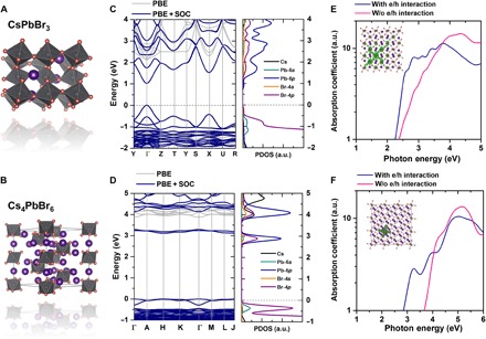
(A and B) Optimized crystal structures. (C and D) Electronic bands and projected density of states (PDOS) calculated at the PBE and PBE + SOC levels (the zero of energy is defined by the VBM in both instances). (E and F) Calculated absorption spectra with and without accounting for electron-hole (e/h) pair interactions together with (see inset) the exciton wave functions (green area) corresponding to the excitonic peaks. a.u., arbitrary units.
The different dispersive features in the conduction and valence bands of the 3D CsPbBr3 and 0D Cs4PbBr6 have important implications regarding carrier effective masses. On the basis of the VBM and CBM around the Γ point, for CsPbBr3, the calculated hole effective mass is mh* = 0.131 m0 along the Γ→Y (−0.5, 0.0, 0.0) direction and mh* = 0.135 m0 along Γ→Z (0.0, 0.0, 0.5); the electron effective mass is slightly larger, with me* = 0.149 m0 (Γ→Y) and me* = 0.142 m0 (Γ→Z), which agrees well with earlier theoretical results (32). In contrast, Cs4PbBr6 shows nearly nondispersive transport along all directions in the electronic bands, which results in heavy charge carriers. In addition, Cs4PbBr6 shows 8.68 × 10⁻⁸ S/m electrical conductivity (σ) in the absence of light irradiation, almost one order of magnitude smaller than CsPbBr3 (7.71 × 10⁻⁷ S/m) (fig. S1A), which agrees well with calculated values of σ/τ for both holes and electrons [Cs4PbBr6, 2 × 10¹⁸ to 5 × 10¹⁸ (ohms·ms)−1 versus CsPbBr3, 3 × 10¹⁹ to 6 × 10¹⁹ (ohms·ms)−1] under the same charge carrier concentration of 1021 cm−3 (see fig. S1B). This is also consistent with the ultralow photocurrent observed in recent experimental work (28), and shows that ion transport has little contribution to the electrical conductivity in 0D perovskites; thus, the low electrical conductivity of Cs4PbBr6 is dominated by electrons and/or holes. Overall, the intrinsic large band gap, heavy charge carriers, and low electrical conductivity of 0D perovskites limit their application in photovoltaic devices.
The differences in crystal phases and band structures of CsPbBr3 and Cs4PbBr6 also generate different absorption spectra and exciton wave function features. Figure 1 (E and F) compares the optical absorption spectra of CsPbBr3 and Cs4PbBr6 calculated at the PBE/SOC level with and without electron-hole interactions [details can be found in the DFT calculations section and in the study of Yin et al. (33)]. In both cases, the main interband electronic transitions related to Pb2+(6s)Br−(4p)→Pb2+(6p) at the Γ point contribute to the higher-energy absorption continuum. Once electron-hole pair interactions are included, in the case of CsPbBr3, the excitonic absorption is weak and the exciton wave function is delocalized over several crystal lattices, which is consistent with its small exciton binding energy (19 to 62 meV) (34, 35). For Cs4PbBr6, the electronic zero dimensionality results in strong quantum confinement, which increases electron-hole interactions and leads to a strong excitonic peak at 3.3 eV and exciton localization on a single [PbBr6]4− octahedron (Fig. 1F). This excitonic peak has been observed in previous experimental absorption measurements at low temperatures (22).
The idea that the weak interactions between neighboring octahedra in 0D crystals cause their properties to be similar to those of individual units is confirmed by time-dependent DFT (TDDFT) calculations on a single Cs4PbBr6 unit. These calculations can reproduce the experimental absorption and capture the absorption features of the Cs4PbBr6 crystal (see Fig. 2A), with a main absorption peak at 320 nm and continuous absorption below 300 nm. Thus, this confirms that a single [PbBr6]4− octahedron reflects the electronic and optical properties of the 0D crystals. In addition, a single unit is an ideal model to study the “molecular” behavior of 0D perovskites, for instance, with regard to the polaronic properties. Upon addition of a charge to ionic and highly polar crystals, such as perovskites (36, 37), the strong Coulomb interactions between the excess charge and the lattice ions enhance the electron-vibration couplings (38). When the excess charges are spatially confined to a volume of approximately one unit cell or less, they are referred to as small polarons, which have been observed in many conjugated polymers upon photo-, electro-, or chemically induced doping (39–41). As shown in Fig. 2B, once an electron is removed from a single Cs4PbBr6 unit, the Pb–Br bond length greatly shortens (from 3.10 to 2.69 Å), and the hole spin density localizes on the Pb atom and the surrounding six Br atoms, indicating the formation of a positively charged polaron (Pb3+). The addition of electrons to the single unit leads to a strongly localized spin density around Pb2+ and large repulsive interactions between Pb and two Br atoms, which markedly elongates these two Pb–Br bonds (from 3.10 to 5.34 Å). Adding an electron to the continuous absorption band below 400 nm, these positive/negative polaronic states (see Fig. 2, B and C) present a new broad absorption feature in the spectral range of 450 to 800 nm, which can thus be assigned to polaron absorption.
Fig. 2. Ground-state and polaron band absorption.
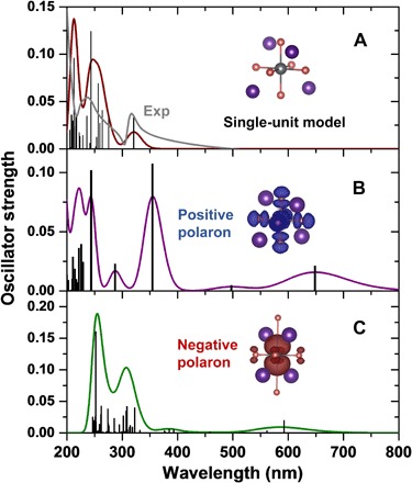
(A) Ground-state absorption of a single Cs4PbBr6 unit and its charged-state absorption for (B) positive and (C) negative polarons, as calculated at the TDDFT level, together with experimental absorption spectra of Cs4PbBr6 thin film (gray line). The spin density distributions are given in the insets.
To further confirm the presence of polarons in 0D perovskites, we performed femtosecond transient absorption (TA) measurements on Cs4PbBr6 and CsPbBr3 thin films. The TA spectra of the CsPbBr3 and Cs4PbBr6 films under identical experimental conditions at different time delays are shown in Fig. 3 (A and B). Here, negative features in the TA spectra correspond to ground-state bleaching (GSB), and broad positive features correspond to PIA, mainly because of the formation of polarons. Similar to the TA spectrum of CsPbBr3, following the excitation wavelength at 310 nm (that is, above the band gap of both samples), the negative band at approximately 515 nm can be attributed to the GSB of the films owing to the depletion of the ground-state carriers to excited states. A new positive broadband appears above 530 nm in the spectrum of the Cs4PbBr6 film owing to polaron absorption, which is completely absent in the CsPbBr3 film. In a 3D perovskite, the excitons can immediately dissociate into free charge carriers because of the small exciton binding energy, which leaves no time for polaron formation. On the other hand, in a way similar to crystalline inorganic materials, adding a charge onto the 3D lattice does not significantly change the surroundings because of the rigid inorganic framework. In this case, a large polaron (Fröhlich polaron) forms because of strong electron-optical phonon coupling, which has optical signatures in a terahertz frequency range (42, 43). However, because a 0D perovskite has a larger exciton binding energy, excitons can hardly dissociate into free charge carriers. Therefore, in a way similar to a polymer system, a 0D perovskite is “soft” (that is, the individual octahedra are easily perturbed by the photoexcitation), which leads to polarons as a new feature present in low-dimensional perovskites. As shown in Fig. 3C, the corresponding kinetics of the polaron absorption band probed at 600 nm shows a lifetime of ~2 ps. This is consistent with the lifetime of polarons observed in pristine polymers (44). Here, the polarons are highly localized on [PbBr6]4− octahedral, and they are likely not to escape but to recombine geminately over a short time.
Fig. 3. TA spectra and polaron kinetics.
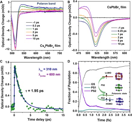
TA spectra of (A) Cs4PbBr6 and (B) Cs4PbBr3 thin films with different delay times at a photoexcitation wavelength of 310 nm. (C) Photoexcitation kinetics of the Cs4PbBr6 film probed at 600 nm about PIA (the solid blue line is the fit for the kinetics using a monoexponential function). (D) Simulated phonon-induced relaxation of the polaronic state (PS1 and PS2) of a single Cs4PbBr6 unit. The frontier molecular energy levels and charge density involved in the excited electron relaxations are given in the inset. HOMO, highest occupied molecular orbital; LUMO, lowest unoccupied molecular orbital; GS, ground-state.
To mimic the experimental pump-probe measurements and elucidate the charge carrier (polaron) relaxation processes in the 0D perovskite, we performed ab initio NAMD simulations on a single Cs4PbBr6 unit by describing the spontaneous transitions among different electronic states (for details, see the “MD calculations” section). As illustrated in Fig. 3D, we assumed that the photogenerated electron could be pumped into unoccupied energy levels through polaronic transitions PS1 and PS2, following an excitation energy of 4 eV. Starting from these two polaronic states in the 0D system, the charge population decays to 10% within a relaxation time of 1.5 ps, which agrees well with the experimental polaron lifetime of ~2 ps. This fast recombination is due to the similar charge distribution features of molecular orbitals involved in the excited electron relaxations (see the insets of Fig. 3D).
Thus, in contrast to the rigid structure of CsPbBr3, the individual [PbBr6]4− octahedra in the 0D crystal can be easily perturbed by photoexcitation processes, leading to polaronic states through structural deformation potentials (local molecular arrangements). Moreover, the discontinuous character of the 0D crystal significantly increases the charge carrier effective masses and strengthens electron-phonon coupling, facilitating small polaron generation, and providing an important optical fingerprint for the polaron band absorption in molecular 0D perovskites.
The single-unit model also allows us to characterize the actual distortions induced by the presence of small polarons. Here, we have evaluated the polaron binding energy (Epolaron) and charge carrier mobility based on molecular Cs4PbBr6 dimers. The positive/negative polaron binding energies (Epolaron) are calculated as 785/943 meV, which are values that are much larger than those in typical π-conjugated systems (45) but smaller than those in some 3D and 2D hybrid perovskites (33, 46). Because the average distance between neighboring [PbBr6]4− octahedra is quite large (~10 Å), a band-like transport mechanism is not suitable for describing the charge carrier mobility of 0D perovskites. Thus, we applied Marcus theory to derive the charge carrier mobilities by describing the charge hopping between neighboring units in molecular dimers. As shown in Fig. 4A, three possible charge hopping paths in the 0D crystal were considered, while the resulting hole mobility of Cs4PbBr6 is calculated to be 1.4 × 10⁻⁹ cm2/V · s, whereas the electron mobility is 2.2 × 10⁻¹¹ cm2/V · s. These low hole/electron mobilities are due to the huge reorganization energies for both holes (1.70 eV) and electrons (2.90 eV), as well as the weak electronic couplings between neighboring units (see table S1). The significantly larger negative polaron binding and reorganization energies of molecular Cs4PbBr6 are related to strong structural deformations (47). As illustrated in Fig. 2, the positive polaronic state preserves the symmetric geometry of the neutral state, while the negative polaronic state leads to extreme elongation of two Pb–Br bonds, breaking the symmetry of the negatively charged [PbBr6]4− octahedron. These calculated values are orders of magnitude smaller than those of the 3D CsPbBr3 perovskite, which has a hole mobility of 52 cm2/V · s and an electron mobility of 11 cm2/V·s (48), and are even lower than those in typical conjugated polymers (for example, P3HT, ~10−4 cm2/V · s). Low charge carrier mobilities become another electronic feature of molecular 0D perovskites, again limiting their applications in optoelectronic devices.
Fig. 4. Polaron transport and localization.
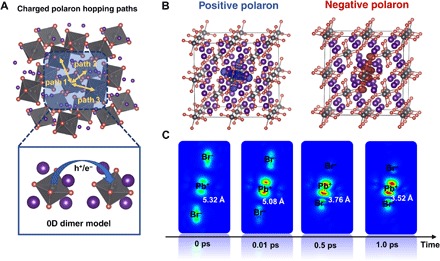
(A) Schematic of charge carrier hopping paths and dimer model for calculating the charge carrier mobility of 0D Cs4PbBr6. (B) Charge density distributions for a 2 × 2 × 2 Cs4PbBr6 supercell with shortened Pb–Br distances (positive polaron) and enlarged Pb–Br distances (negative polaron) within the central [PbBr6]4− octahedron. (C) Charge density mapping of CBM of the central octahedron at selected times (0, 0.01, 0.05, 0.1, 0.5, and 1.0 ps). The initial state at 0 ps was set as the negative-polaron state and had the longest Pb–Br bonds in the central octahedron. The selected Pb–Br bond lengths are indicated in each time delay.
To examine the small polaron features in bulk Cs4PbBr6 perovskites, following the same computational strategy as in our previous work on 2D hybrid perovskites (33), we exerted local perturbations on 2 × 2 × 2 Cs4PbBr6 supercells, where the selected Pb–Br bond lengths of the central [PbBr6]4− unit were shortened or enlarged to create local structural deformations. Figure 4B illustrates the resulting electronic charge densities at the VBM and CBM after local structural perturbations. In the unperturbed systems, the charge densities of the VBM and CBM are highly delocalized in all octahedra (see fig. S2). Once the Pb–Br bonds of the central [PbBr6]4− unit are shortened, the hole charge density (blue area) localizes at the central site, leading to the formation of Pb3+ centers coupled with the lattice deformation. Similarly, in the case of enlarged Pb–Br bonds, the electron charge density (red area) is also localized at the central [PbBr6]4−. As we already demonstrated in the model for the polaronic state of a single unit, the strong interaction between charge carriers and phonons yields the formation of both self-trapped electron and hole states in the 0D crystal, which is in good agreement with previous experimental observations in low-dimensional lead halides (49–51).
On the basis of the perturbed supercell model for describing polaron localization in the 0D crystal, we further performed ab initio MD calculations to study local structural changes and the evolution of the charge density at a central [PbBr6]4− octahedron. As shown in Fig. 4C and fig. S3, upon release from the initial state (for example, polaronic state with the longest Pb–Br bonds), the average Pb–Br bond length decreased, and the CBM energy level increased within the first 1 ps. During this time, the CBM charge density is still localized at the central octahedron, and the Pb–Br bond lengths and CBM energy undergo thermal fluctuations at room temperature. After 1.2 ps, the central octahedron recovers to the neutral state. Therefore, after photoexcitation, the structure deformation of single octahedra leads to the formation of localized polarons with short lifetime and limited transport in the 0D crystal. In addition, although the positive and negative polarons have similar absorption features (Fig. 2), the lifetime of a positive polaron could be even shorter than the negative one because of the faster recovery (within 0.1 ps) of Pb–Br bonds and corresponding VBM energy (fig. S3).
In summary, we studied the molecular behavior of the 0D Cs4PbBr6 perovskite by combining DFT calculations and femtosecond transition absorption measurements. Unlike 3D CsPbBr3, 0D Cs4PbBr6 displays a large band gap, as well as low electrical conductivity and charge carrier mobility. A clear spectral feature for polarons with a short lifetime of ~2 ps is observed in the femtosecond-TA experiments, confirming the generation of small polarons with large binding energies and tight localization at individual [PbBr6]4− octahedra. These findings provide a better understanding of the fundamental photophysical properties of 0D perovskites and open up new avenues for the rational design of low-dimensional perovskites in optoelectronic devices.
MATERIALS AND METHODS
DFT calculations
DFT calculations were performed to optimize the crystal structures of CsPbBr3 and Cs4PbBr6 using the PWSCF code, as implemented in the Quantum ESPRESSO (QE) package (52). The PBE exchange-correlation functional with ultrasoft pseudopotentials was used with and without consideration of SOC. Plane-wave basis set cutoffs for the wave functions and charge density were set at 50 and 300 rydberg (Ry), respectively. The crystal structures were fully relaxed until the total force on each atom was less than 0.01 eV/Å. A uniform grid of 6 × 6 × 6 k-mesh in the Brillouin zone was used to obtain the electronic band structures and projected density of states for both crystals. A dense k-mesh (24 × 24 × 24) was used to obtain the electrical transport coefficients with the BoltzTraP package (53). On the basis of the electronic wave functions of the ground state obtained by the QE code, the optical transitions of CsPbBr3 and Cs4PbBr6 were calculated using both the random-phase approximation and the Bethe-Salpeter equation approach implemented in the YAMBO code (54). In this case, PBE calculations were performed by using norm-conserving pseudopotentials including SOC effects and plane-wave basis set cutoffs of 80 Ry (400 Ry) for the wave function (charge density) (33).
For the single Cs4PbBr6 unit, the neutral and charged geometries were optimized with the hybrid range-corrected functional CAM-B3LYP using the Gaussian 09 code. The LANL2DZ basis set was used for Cs and Pb atoms, and the 6-31G** basis set was used to describe Br. On the basis of the optimized geometries in both the ground and polaronic states, the PBE0 hybrid functional was used to obtain the optical absorption spectra using the TDDFT method. A total of 200 singlet states were considered in describing the possible optical transitions.
The charge transfer rates between neighboring octahedra were described by Marcus theory (55, 56) following the equation , where T is the temperature, kB and ℏ refer to the Boltzmann and Planck constants, Vh/e is the electronic coupling between the HOMO or LUMO levels of neighboring octahedra in the Cs4PbBr6 dimers, and λh/e is the hole or electron reorganization energy calculated via the adiabatic potential energy surfaces. Vij is the electronic coupling, defined as , which can be calculated by projecting the Fock matrix of the dimer onto the molecular orbitals of the respective donor (φi) and acceptor (φj) units with subsequent symmetric orthogonalization, where is the Kohn-Sham Fock operator for the dimer system. The hole or electron mobility was then described by the Einstein relation (57), where e is the electron charge and D is the charge diffusion coefficient of charge carriers, which can be approximately described as , where ki and ri are the charge-transfer rate and the neighboring distance for the dimer and Pi represents the probability for hole/electron hopping in the ith pathway.
MD calculations
Adiabatic ab initio MD calculations were also performed using the QE code with the PBE functional and ultrasoft pseudopotential. The optimized crystal structure of the 2 × 2 × 2 Cs4PbBr6 supercell was used as the starting point for the adiabatic MD calculations, where a 5-ps trajectory of the system was obtained with 1-fs time steps. The Andersen thermostat was used to control the temperature of the system.
NAMD calculations on a single Cs4PbBr6 unit were performed using the PYXAID code (58, 59) developed by Akimov and Prezhdo. In this code, fewest-switches surface hopping (60) implemented within TDDFT was used to study the hybrid perovskite system (61–63), starting from the time-dependent Schrödinger equation and Kohn-Sham orbitals . From the solutions of these equations, the probability of transition between adiabatic states i and j can be calculated using the wave function expansion coefficients and coupling, defined as . The detailed descriptions of this NAMD theory can be found in the study of Akimov and Prezhdo (58, 59). Here, we used the real-time TDDFT/NAMD method with decoherence effects on a single Cs4PbBr6 unit. A total of 1000 geometries were randomly selected from the adiabatic trajectories and used as initial conditions in the NAMD calculations.
Preparation of 0D and 3D perovskite films
Three-dimensional CsPbBr3 and 0D Cs4PbBr6 thin films were deposited on glass substrates precleaned with acetone/isopropanol. CsPbBr3 was deposited by spin-coating a 0.25 M solution of CsBr and PbBr2 in dimethyl sulfoxide, dripped with toluene, and followed by thermal annealing at 100°C for 10 min. The Cs4PbBr6 thin film was deposited through the vacuum thermal evaporation (1 × 10⁻⁶ mbar) of Cs4PbBr6 powder (16), with a final thickness of 100 nm. The samples were fabricated and stored in a nitrogen-filled glove box. The materials and solvents were provided by Sigma-Aldrich and used without further purification. The experimental x-ray diffraction patterns of CsPbB3 and Cs4PbBr6 thin films are shown in fig. S4.
Electrical conductivity measurements
The electrical conductivity was determined by investigating the dark current/voltage characteristics of CsPbBr3 and Cs4PbBr6 thin films on commercial interdigitated substrates with a channel width-to-length ratio of 2000 μm/2.5 μm (Fraunhofer Institute for Photonic Microsystems).
Femtosecond TA spectroscopy
The time-resolved experiments were conducted on ExciPro pump-probe spectrometers (CDP), in which the fundamental output came from a Ti:sapphire femtosecond regenerative amplifier operating at 800 nm with 35-fs pulses and a 1-kHz repetition rate. Pump pulses at 310 nm were generated after passing through a fraction of the 800-nm beam into a spectrally tunable (240 to 2600 nm) optical parametric amplifier (TOPAS Prime, Spectra-Physics) and a frequency mixer (NirUVis, Light Conversion). To generate the probe pulses (ultraviolet-visible and near-infrared wavelength continuum, white light), another fraction of 800 nm–amplified pulses was focused onto 2-mm-thick calcium fluoride (CaF2) crystal. To achieve better signal-to-noise ratios, the resulting white light was split into two channels, denoted the probe and reference, and focused on the two different fiber optics. The pump pulses were overlapped on the sample with the probe pulses after passing through a synchronized chopper (500 Hz), which blocked alternative pump pulses. Finally, the change in absorption (ΔA) of the excited state was calculated by subtracting the absorptions of the excited and unexcited samples.
Supplementary Material
Acknowledgments
J.Y., J.-L.B., and O.F.M. acknowledge the IT Research Computing Team and Supercomputing Laboratory at KAUST for their computational and storage resources, as well as their assistance. Funding: This work was supported by the King Abdullah University of Science and Technology (KAUST). The work at Georgia Tech was funded by the Office of Naval Research, Award NO. N00014-17-1-2208. Author contributions: J.Y. generated the idea and designed the simulation work. O.M.B. and O.F.M. crafted the experimental plan and directed the research. J.Y. performed all the ab initio calculations. J.Y., J.-L.B., and O.F.M. analyzed the theoretical results. M.D.B. and I.D. prepared the thin film samples and measured the electrical conductivity. P.M. and O.F.M. planned and performed the TA spectrum measurements and analyzed the data. J.Y., J.-L.B., and O.F.M. wrote the manuscript. All authors discussed and commented on the manuscript. Competing interests: The authors declare that they have no competing interests. Data and materials availability: All data needed to evaluate the conclusions in the paper are present in the paper and/or the Supplementary Materials. Additional data related to this paper may be requested from the authors.
SUPPLEMENTARY MATERIALS
Supplementary material for this article is available at http://advances.sciencemag.org/cgi/content/full/3/12/e1701793/DC1
fig. S1. Experimental and calculated electrical conductivity of CsPbB3 and Cs4PbBr6.
fig. S2. Charge density descriptions of Cs4PbBr6 supercell.
fig. S3. Average Pb–Br bond length and orbital energy evolution.
fig. S4. X-ray diffraction patterns of CsPbB3 and Cs4PbBr6 thin films.
table S1. Calculated charge transfer parameters and mobility of the Cs4PbBr6 crystal.
REFERENCES AND NOTES
- 1.Protesescu L., Yakunin S., Bodnarchuk M. I., Krieg F., Caputo R., Hendon C. H., Yang R. X., Walsh A., Kovalenko M. V., Nanocrystals of cesium lead halide perovskites (CsPbX3, X = Cl, Br, and I): Novel optoelectronic materials showing bright emission with wide color gamut. Nano Lett. 15, 3692–3696 (2015). [DOI] [PMC free article] [PubMed] [Google Scholar]
- 2.Nedelcu G., Protesescu L., Yakunin S., Bodnarchuk M. I., Grotevent M. J., Kovalenko M. V., Fast anion-exchange in highly luminescent nanocrystals of cesium lead halide perovskites (CsPbX3, X = Cl, Br, I). Nano Lett. 15, 5635–5640 (2015). [DOI] [PMC free article] [PubMed] [Google Scholar]
- 3.Song J., Li J., Li X., Xu L., Dong Y., Zeng H., Quantum dot light-emitting diodes based on inorganic perovskite cesium lead halides (CsPbX3). Adv. Mater. 27, 7162–7167 (2015). [DOI] [PubMed] [Google Scholar]
- 4.Bekenstein Y., Koscher B. A., Eaton S. W., Yang P., Alivisatos A. P., Highly luminescent colloidal nanoplates of perovskite cesium lead halide and their oriented assemblies. J. Am. Chem. Soc. 137, 16008–16011 (2015). [DOI] [PubMed] [Google Scholar]
- 5.Yakunin S., Protesescu L., Krieg F., Bodnarchuk M. I., Nedelcu G., Humer M., De Luca G., Fiebig M., Heiss W., Kovalenko M. V., Low-threshold amplified spontaneous emission and lasing from colloidal nanocrystals of caesium lead halide perovskites. Nat. Commun. 6, 8056 (2015). [DOI] [PMC free article] [PubMed] [Google Scholar]
- 6.Pan J., Sarmah S. P., Murali B., Dursun I., Peng W., Parida M. R., Liu J., Sinatra L., Alyami N., Zhao C., Alarousu E., Ng T. K., Ooi B. S., Bakr O. M., Mohammed O. F., Air-stable surface-passivated perovskite quantum dots for ultra-robust, single- and two-photon-induced amplified spontaneous emission. J. Phys. Chem. Lett. 6, 5027–5033 (2015). [DOI] [PubMed] [Google Scholar]
- 7.Ramasamy P., Lim D.-H., Kim B., Lee S.-H., Lee M.-S., Lee J.-S., All-inorganic cesium lead halide perovskite nanocrystals for photodetector applications. Chem. Commun. 52, 2067–2070 (2016). [DOI] [PubMed] [Google Scholar]
- 8.Zhang D., Eaton S. W., Yu Y., Dou L., Yang P., Solution-phase synthesis of cesium lead halide perovskite nanowires. J. Am. Chem. Soc. 137, 9230–9233 (2015). [DOI] [PubMed] [Google Scholar]
- 9.Zhu H., Miyata K., Fu Y., Wang J., Joshi P. P., Niesner D., Williams K. W., Jin S., Zhu X.-Y., Screening in crystalline liquids protects energetic carriers in hybrid perovskites. Science 353, 1409–1413 (2016). [DOI] [PubMed] [Google Scholar]
- 10.Jellicoe T. C., Richter J. M., Glass H. F. J., Tabachnyk M., Brady R., Dutton S. E., Rao A., Friend R. H., Credgington D., Greenham N. C., Böhm M. L., Synthesis and optical properties of lead-free cesium tin halide perovskite nanocrystals. J. Am. Chem. Soc. 138, 2941–2944 (2016). [DOI] [PubMed] [Google Scholar]
- 11.Sarmah S. P., Burlakov V. M., Yengel E., Murali B., Alarousu E., El-Zohry A. M., Yang C., Alias M. S., Zhumekenov A. A., Saidaminov M. I., Cho N., Wehbe N., Mitra S., Ajia I., Dey S., Mansour A. E., Abdelsamie M., Amassian A., Roqan I. S., Ooi B. S., Goriely A., Bakr O. M., Mohammed O. F., Double charged surface layers in lead halide perovskite crystals. Nano Lett. 17, 2021–2027 (2017). [DOI] [PubMed] [Google Scholar]
- 12.Bisquert J., Qi Y., Ma T., Yan Y., Advances and obstacles on perovskite solar cell research from material properties to photovoltaic function. ACS Energy Lett. 2, 520–523 (2017). [Google Scholar]
- 13.Cortecchia D., Neutzner S., Kandada A. R. S., Mosconi E., Meggiolaro D., De Angelis F., Soci C., Petrozza A., Broadband emission in two-dimensional hybrid perovskites: The role of structural deformation. J. Am. Chem. Soc. 139, 39–42 (2017). [DOI] [PubMed] [Google Scholar]
- 14.Blancon J.-C., Tsai H., Nie W., Stoumpos C. C., Pedesseau L., Katan C., Kepenekian M., Soe C. M. M., Appavoo K., Sfeir M. Y., Tretiak S., Ajayan P. M., Kanatzidis M. G., Even J., Crochet J. J., Mohite A. D., Extremely efficient internal exciton dissociation through edge states in layered 2D perovskites. Science 355, 1288–1292 (2017). [DOI] [PubMed] [Google Scholar]
- 15.Bark O. M., Mohammed O. F., Powering up perovskite photoresponse. Science 355, 1260–1261 (2017). [DOI] [PubMed] [Google Scholar]
- 16.Saidaminov M. I., Almutlaq J., Sarmah S., Dursun I., Zhumekenov A. A., Begum R., Pan J., Cho N., Mohammed O. F., Bakr O. M., Pure Cs4PbBr6: Highly luminescent zero-dimensional perovskite solids. ACS Energy Lett. 1, 840–845 (2016). [Google Scholar]
- 17.Cheng Z., Lin J., Layered organic–inorganic hybrid perovskites: Structure, optical properties, film preparation, patterning and templating engineering. CrystEngComm 12, 2646–2662 (2010). [Google Scholar]
- 18.Andrews R. H., Clark S. J., Donaldson J. D., Dewan J. C., Silver J., Solid-state properties of materials of the type-Cs4MX6 (where M = Sn or Pb and X = Cl or Br). J. Chem. Soc. Dalton Trans. 0, 767.– (1983). [Google Scholar]
- 19.Nikl M., Mihokova E., Nitsch K., Photoluminescence and decay kinetics of Cs4PbCl6 single crystals. Solid State Commun. 84, 1089–1092 (1992). [Google Scholar]
- 20.Nikl M., Mihokova E., Nitsch K., Somma F., Giampaolo C., Pazzi G. P., Fabeni P., Zazubovich S., Photoluminescence of Cs4PbBr6 crystals and thin films. Chem. Phys. Lett. 306, 280–284 (1999). [Google Scholar]
- 21.Kondo S., Amaya K., Higuchi S., Saito T., Asada H., Ishikane M., Fundamental optical absorption of Cs4PbCl6. Solid State Commun. 120, 141–144 (2001). [Google Scholar]
- 22.Kondo S., Amaya K., Saito T., Localized optical absorption in Cs4PbBr6. J. Phys. Condens. Matter 14, 2093–2099 (2002). [Google Scholar]
- 23.Kondo S., Masaki A., Saito T., Asada H., Fundamental optical absorption of CsPbI3 and Cs4PbI6. Solid State Commun. 124, 211–214 (2002). [Google Scholar]
- 24.Yunakova O. N., Miloslavskii V. K., Kovalenko E. N., Exciton absorption spectrum of thin CsPbI3 and Cs4PbI6 films. Opt. Spectrosc. 112, 91–96 (2012). [Google Scholar]
- 25.Akkerman Q. A., Park S., Radicchi E., Nunzi F., Mosconi E., De Angelis F., Brescia R., Rastogi P., Prato M., Manna L., Nearly monodisperse insulator Cs4PbX6 (X = Cl, Br, I) nanocrystals, their mixed halide compositions, and their transformation into CsPbX3 nanocrystals. Nano Lett. 17, 1924–1930 (2017). [DOI] [PMC free article] [PubMed] [Google Scholar]
- 26.Zhang Y., Saidaminov M. I., Dursun I., Yang H., Murali B., Alarousu E., Yengel E., Alshankiti B. A., Bakr O. M., Mohammed O. F., Zero-dimensional Cs4PbBr6 perovskite nanocrystals. J. Phys. Chem. Lett. 8, 961–965 (2017). [DOI] [PubMed] [Google Scholar]
- 27.Huang K., Li D., Yang L., Liu S., Yang F., Solution-processed approach to highly luminescent trigonal Cs4PbBr6 nanodisks and their underlying shape evolution. J. Alloys Compd. 710, 244–252 (2017). [Google Scholar]
- 28.Cha J.-H., Han J. H., Yin W., Park C., Park Y., Ahn T. K., Cho J. H., Jung D.-Y., Photoresponse of CsPbBr3 and Cs4PbBr6 perovskite single crystals. J. Phys. Chem. Lett. 8, 565–570 (2017). [DOI] [PubMed] [Google Scholar]
- 29.Xiao Z., Meng W., Wang J., Mitzi D. B., Yan Y., Searching for promising new perovskite-based photovoltaic absorbers: The importance of electronic dimensionality. Mater. Horiz. 4, 206–216 (2017). [Google Scholar]
- 30.Umari P., Mosconi E., De Angelis F., Relativistic GW calculations on CH3NH3PbI3 and CH3NH3SnI3 perovskites for solar cell applications. Sci. Rep. 4, 4467 (2014). [DOI] [PMC free article] [PubMed] [Google Scholar]
- 31.Stoumpos C. C., Malliakas C. D., Peters J. A., Liu Z., Sebastian M., Im J., Chasapis T. C., Wibowo A. C., Chung D. Y., Freeman A. J., Wessels B. W., Kanatzidis M. G., Crystal growth of the perovskite semiconductor CsPbBr3: A new material for high-energy radiation detection. Cryst. Growth Des. 13, 2722–2727 (2013). [Google Scholar]
- 32.Chang Y. H., Park C. H., Matsuishi K., First-principles study of the structural and the electronic properties of the lead-halide-based inorganic–organic perovskites (CH3NH3)PbX3 and CsPbX3 (X = Cl, Br, I). J. Korean Phys. Soc. 44, 889–893 (2004). [Google Scholar]
- 33.Yin J., Li H., Cortecchia D., Soci C., Brédas J.-L., Excitonic and polaronic properties of 2D hybrid organic–inorganic perovskites. ACS Energy Lett. 2, 417–423 (2017). [Google Scholar]
- 34.Yettapu G. R., Talukdar D., Sarkar S., Swarnkar A., Nag A., Ghosh P., Mandal P., Terahertz conductivity within colloidal CsPbBr3 perovskite nanocrystals: Remarkably high carrier mobilities and large diffusion lengths. Nano Lett. 16, 4838–4848 (2016). [DOI] [PubMed] [Google Scholar]
- 35.Li J., Yuan X., Jing P., Li J., Wei M., Hua J., Zhao J., Tian L., Temperature-dependent photoluminescence of inorganic perovskite nanocrystal films. RSC Adv. 6, 78311–78316 (2016). [Google Scholar]
- 36.Zhu X.-Y., Podzorov V., Charge carriers in hybrid organic–inorganic lead halide perovskites might be protected as large polarons. J. Phys. Chem. Lett. 6, 4758–4761 (2015). [DOI] [PubMed] [Google Scholar]
- 37.D. Emin, Polarons (Cambridge Univ. Press; 2013). [Google Scholar]
- 38.Chen Y., Yi H. T., Wu X., Haroldson R., Gartstein Y. N., Rodionov Y. I., Tikhonov K. S., Zakhidov A., Zhu X.-Y., Podzorov V., Extended carrier lifetimes and diffusion in hybrid perovskites revealed by Hall effect and photoconductivity measurements. Nat. Commun. 7, 12253 (2016). [DOI] [PMC free article] [PubMed] [Google Scholar]
- 39.Bredas J. L., Street G. B., Polarons, bipolarons, and solitons in conducting polymers. Acc. Chem. Res. 18, 309–315 (1985). [Google Scholar]
- 40.Zaikowski L., Kaur P., Gelfond C., Selvaggio E., Asaoka S., Wu Q., Chen H.-C., Takeda N., Cook A. R., Yang A., Rosanelli J., Miller J. R., Polarons, bipolarons, and side-by-side polarons in reduction of oligofluorenes. J. Am. Chem. Soc. 134, 10852–10863 (2012). [DOI] [PubMed] [Google Scholar]
- 41.Österbacka R., An C. P., Jiang X. M., Vardeny Z. V., Two-dimensional electronic excitations in self-assembled conjugated polymer nanocrystals. Science 287, 839–842 (2000). [DOI] [PubMed] [Google Scholar]
- 42.Emin D., Optical properties of large and small polarons and bipolarons. Phys. Rev. B 48, 13691–13702 (1993). [DOI] [PubMed] [Google Scholar]
- 43.Miyata K., Meggiolaro D., Trinh M. T., Joshi P. P., Mosconi E., Jones S. C., De Angelis F., Zhu X.-Y., Large polarons in lead halide perovskites. Sci. Adv. 3, e1701217 (2017). [DOI] [PMC free article] [PubMed] [Google Scholar]
- 44.Miranda P. B., Moses D., Heeger A. J., Ultrafast photogeneration of charged polarons in conjugated polymers. Phys. Rev. B 64, 081201 (2001). [Google Scholar]
- 45.Coropceanu V., Cornil J., da Silva Filho D. A., Olivier Y., Silbey R., Brédas J.-L., Charge transport in organic semiconductors. Chem. Rev. 107, 926–952 (2007). [DOI] [PubMed] [Google Scholar]
- 46.Neukirch A. J., Nie W. Y., Blancon J.-C., Appavoo K., Tsai H., Sfeir M. Y., Katan C., Pedesseau L., Even J., Crochet J. J., Gupta G., Mohite A. D., Tretiak S., Polaron stabilization by cooperative lattice distortion and cation rotations in hybrid perovskite materials. Nano Lett. 16, 3809–3816 (2016). [DOI] [PubMed] [Google Scholar]
- 47.Sánchez-Carrera R. S., Coropceanu V., Kim E.-G., Brédas J.-L., Charge-transport properties of the 1,4-diiodobenzene crystal: A quantum-mechanical study. Chem. Mater. 20, 5832–5838 (2008). [Google Scholar]
- 48.Saidaminov M. I., Haque M. A., Almutlaq J., Sarmah S., Miao X.-H., Begum R., Zhumekenov A. A., Dursun I., Cho N., Murali B., Mohammed O. F., Wu T., Bakr O. M., Inorganic lead halide perovskite single crystals: Phase-selective low-temperature growth, carrier transport properties, and self-powered photodetection. Adv. Opt. Mater. 5, 1600704 (2017). [Google Scholar]
- 49.Nistor S. V., Schoemaker D., Consistent analysis of the Tl2+ and Pb23+ center ESR parameters. Phys. Stat. Sol. (b) 190, 339–346 (1995). [Google Scholar]
- 50.Nistor S. V., Goovaerts E., Schoemaker D., Direct observation of electron self-trapping in PbCl2 crystals. Phys. Rev. B 48, 9575–9580 (1993). [DOI] [PubMed] [Google Scholar]
- 51.Iwanaga M., Azuma J., Shirai M., Tanaka K., Hayashi T., Self-trapped electrons and holes in PbBr2 crystals. Phys. Rev. B 65, 214306 (2002). [Google Scholar]
- 52.Giannozzi P., Baroni S., Bonini N., Calandra M., Car R., Cavazzoni C., Ceresoli D., Chiarotti G. L., Cococcioni M., Dabo I., Dal Corso A., de Gironcoli S., Fabris S., Fratesi G., Gebauer R., Gerstmann U., Gougoussis C., Kokalj A., Lazzeri M., Martin-Samos L., Marzari N., Mauri F., Mazzarello R., Paolini S., Pasquarello A., Paulatto L., Sbraccia C., Scandolo S., Sclauzero G., Seitsonen A. P., Smogunov A., Umari P., Wentzcovitch R. M., QUANTUM ESPRESSO: A modular and open-source software project for quantum simulations of materials. J. Phys. Condens. Matter 21, 395502 (2009). [DOI] [PubMed] [Google Scholar]
- 53.Madsen G. K. H., Singh D. J., BoltzTraP. A code for calculating band-structure dependent quantities. Comput. Phys. Commun. 175, 67–71 (2006). [Google Scholar]
- 54.Marini A., Hogan C., Grüning M., Varsano D., Yambo: An ab initio tool for excited state calculations. Comput. Phys. Commun. 180, 1392–1403 (2009). [Google Scholar]
- 55.Marcus R. A., Electron transfer reactions in chemistry. Theory and experiment. Rev. Mod. Phys. 65, 599–610 (1993). [Google Scholar]
- 56.Marcus R. A., Sutin N., Electron transfers in chemistry and biology. Biochim. Biophys. Acta 811, 265–322 (1985). [Google Scholar]
- 57.Yin J., Chen R.-F., Zhang S.-L., Li H.-H., Zhang G.-W., Feng X.-M., Ling Q.-D., Huang W., Theoretical study of charge-transfer properties of the π-stacked poly(1,1-silafluorene)s. J. Phys. Chem. C 115, 14778–14785 (2011). [Google Scholar]
- 58.Akimov A. V., Prezhdo O. V., The PYXAID program for non-adiabatic molecular dynamics in condensed matter systems. J. Chem. Theory Comput. 9, 4959–4972 (2013). [DOI] [PubMed] [Google Scholar]
- 59.Akimov A. V., Prezhdo O. V., Advanced capabilities of the PYXAID program: Integration schemes, decoherence effects, multiexcitonic states, and field-matter interaction. J. Chem. Theory Comput. 10, 789–804 (2014). [DOI] [PubMed] [Google Scholar]
- 60.Tully J. C., Molecular dynamics with electronic transitions. J. Chem. Phys. 93, 1061–1071 (1990). [Google Scholar]
- 61.Liu J., Prezhdo O. V., Chlorine doping reduces electron–hole recombination in lead iodide perovskites: Time-domain ab initio analysis. J. Phys. Chem. Lett. 6, 4463–4469 (2015). [DOI] [PubMed] [Google Scholar]
- 62.Long R., Liu J., Prezhdo O. V., Unravelling the effects of grain boundary and chemical doping on electron–hole recombination in CH3NH3PbI3 perovskite by time-domain atomistic simulation. J. Am. Chem. Soc. 138, 3884–3890 (2016). [DOI] [PubMed] [Google Scholar]
- 63.Long R., Fang W., Prezhdo O. V., Moderate humidity delays electron–hole recombination in hybrid organic–inorganic perovskites: Time-domain ab initio simulations rationalize experiments. J. Phys. Chem. Lett. 7, 3215–3222 (2016). [DOI] [PubMed] [Google Scholar]
Associated Data
This section collects any data citations, data availability statements, or supplementary materials included in this article.
Supplementary Materials
Supplementary material for this article is available at http://advances.sciencemag.org/cgi/content/full/3/12/e1701793/DC1
fig. S1. Experimental and calculated electrical conductivity of CsPbB3 and Cs4PbBr6.
fig. S2. Charge density descriptions of Cs4PbBr6 supercell.
fig. S3. Average Pb–Br bond length and orbital energy evolution.
fig. S4. X-ray diffraction patterns of CsPbB3 and Cs4PbBr6 thin films.
table S1. Calculated charge transfer parameters and mobility of the Cs4PbBr6 crystal.