Abstract
This paper describes a reproducible method for μm precision alignment of polydimethylsiloxane (PDMS) microchannels with coplanar electrodes using a conventional mask aligner for lab-on-a-chip applications. It is based on the use of a silicon mold in combination with a PMMA sarcophagus for precise control of the parallelism between the top and bottom surfaces of molded PDMS. The alignment of the fabricated PDMS slab with electrodes patterned on a glass chip is then performed using a conventional mask aligner with a custom-made steel chuck and magnets. This technique allows to bond and align chips with a resolution of less than 2 μm.
I. INTRODUCTION
Polydimethylsiloxane (PDMS) is a polymer widely used in microfluidics. Its main advantages are that it is optically transparent, low-cost, chemically resistant to many solvents, easily bondable to itself and other materials and commercially available.1 This polymer enables 3D fabrication of nano or microscale structures by replica molding from a master that can be created in various materials like SU-8, Si, or PMMA, or by using PDMS as a sensitive photoresist after the addition of various photoinitiators.2,3 In the field of lab-on-chip (LOC) systems, there are many situations in which a PDMS structure should be bonded to a patterned substrate after an air or oxygen plasma treatment. This operation may require precise alignment between the different layers, which can be quite challenging. Alignment may, for instance, be a concern in a PDMS multilayer assembly, an approach widely used for the fabrication of 3D organ-on-a-chip platforms. For example, Huh et al.4 have designed a lung-on-a-chip system consisting of two side channels and a main channel divided by a porous membrane, obtained by stacking and bonding of three PDMS layers. Mechanical stretching of the membrane is ensured by applying vacuum to side chambers, in order to mimic the lung breathing movements. Here, a misalignment between the different PDMS stacks would result in vacuum leakage and operational failure.
This issue is also particularly relevant for LOC applications, implying integration of electrodes within a microfluidic chip, such as electrochemical sensors,5 cultured neuronal networks,6 microfluidic sorters based on surface acoustic waves,7 or dielectrophoresis,8 capillary electrophoresis chips,9 etc. To circumvent this technical difficulty, one approach consists of replacing the structured PDMS by a thick photoresist layer like SU-8 that can be patterned and aligned on the top of electrodes using standard photolithography process, as proposed by Demierre et al.10 The use of SU-8 enables to obtain microchannels with a high Young's modulus that will not deform easily and allow precise alignment with structures already present at the wafer scale.11 However, SU-8 is less prevalent for prototyping in microfluidics compared with PDMS. This can be partially explained by challenges encountered by SU-8 users such as adhesion issues, a high sensitivity of the SU-8 polymerization to humidity as well as the question of microchannel sealing with other materials such as PDMS with mechanical clamping or irreversible bonding.12,13
In some cases, there may also be a requirement for aligning PDMS stamps with electrodes, as described by Menad et al.14 who used bond-detach lithography to form selective openings in a thin PDMS layer covering an electrode array, thereby modifying the electric field pattern generated.
Another typical example where proper alignment is required is that of microfluidic chips dedicated to impedance spectroscopy. In such devices, the position of the sensing electrodes in the microchannel will, due to their shape, influence the detected signal and the distribution of the electric field, which may cause a wrong interpretation of the particle size and properties.15
A necessary step prior to alignment is the PDMS shrinkage compensation. PDMS shrinkage occurs when it is cured and depends mostly on the cure temperature and time, the PDMS components ratio, and the layer thickness. To overcome these problems, some authors proposed to avoid this shrinkage by either curing the PDMS at room temperature or to keep the soft PDMS always in bound with a stiff substrate.16,17 Curing at room temperature will decrease mechanical properties and will be very sensitive to small changes in temperature.18 Using a stiff substrate always in contact with the PDMS requires to perform some alignment between layers when the PDMS is transferred on another patterned substrate.19 By precisely characterizing the shrinkage, Lee et al.20 proposed a scaling factor to be applied to the mold during fabrication. In this case, the shrinkage has to be properly characterized for the specific conditions where the mold is used.
Another important requirement is to ensure that the parallelism between the top and bottom surfaces of molded PDMS is effective as well as their flatness, as stated by Li,21 otherwise, the contact between the PDMS and the electrodes will not happen at exactly the same time on the surface and thus will lead to misalignment errors. Land et al.22 proposed to use a PMMA assembly where the thickness of a PMMA part will control the thickness of the PDMS and the flatness and parallelism of the surfaces will be ensured by a top PMMA part used as a smoothing jig. However, the closure may lead to the trapping of a thin PDMS layer between the PDMS parts which might reduce the control on the PDMS surface parallelism.
Different alignment methods were proposed in the literature, the simplest one being to carry out a manual alignment under a microscope, based on visible structures on the chip,23 but it is rather limited in terms of both precision and reproducibility.24 Another approach is to use mechanical jigs25 to improve the alignment, but it requires additional structural features and the thickness variability of the different layers will limit the alignment precision. Most systems in the literature intend to reproduce the conventional mask aligner used in the cleanroom facilities that allows both alignment between two different levels and a pressure control of the bonding. Kim et al.24 proposed a system based on a stereomicroscope and holding pins to hold the top PDMS slab, thereby overcoming the problem of non-uniformity of the PDMS layer. Its effectiveness is, however, restricted to a small area because it is limited to the field of view of the stereomicroscope (< 1 cm). An alternative approach was proposed by Sivakumarasamy et al.26,27 and is based on PDMS adhesion on an accessory placed on a microscope objective that allows precise and reliable alignment. However, the tool used limits the alignment to the central zone which might complicate the correction of the tilt if alignment of distant patterns is required. Li et al.28 proposed a custom-built desktop aligner capable of both local and global alignments. This instrument is based on two digital microscopes with a resolution of 20 μm/cm to perform the alignment on structures up to 4 in. in size but this requires one to build a new machine and to calibrate it. More recently, an automatic multilayered integrated microfluidic device fabrication has been proposed by Kipper et al.29 and relies on computerized control of the alignment between the different layers before contact to reach an average alignment resolution of 1 μm/cm. However, those approaches require the construction and calibration of a dedicated machine.
Combining all the critical aspects together, from the control of the PDMS properties (the parallelism between the surfaces, surface flatness, shrinkage compensation, and thickness) to the alignment of the PDMS slab with electrodes, is necessary to perform a reproducible alignment. Partial elements are presented in the literature, but there remains a need for a systematic approach addressing all these issues at once.
In this article, we describe a full process for fabricating a PDMS slab with microfluidic features and a glass chip with patterned electrodes and aligning them with a conventional mask aligner with a resolution of more than 10 μm/cm on structures up to 4 in. For the sake of illustration, this process is applied to the fabrication of a dielectrophoretic focusing and electro-orientation module composed of liquid electrodes,30 which are coplanar electrodes positioned at the bottom of dead-end chambers placed on each side of the main channel. This module will be inserted upstream of the detection zone of an impedance-based flow cytometer, as previously described by Shaker et al.31
II. METHODS
A. Fabrication
1. Process flow
a. Electrode fabrication
Electrodes are fabricated through a standard photolithography process. After a Piranha bath treatment, 20 nm of titanium and then 200 nm of platinum are sputtered on a 4 in. float glass wafer. 1.5 μm of a positive photoresist AZ1512 is then coated with an automatic wafer coater and developer, the ACS 200 (SUSS MicroTec—Garching, Germany), and subsequently structured by means of direct writing with a WaferWriter MLA150 (Heidelberg Instrument—Heidelberg, Germany) before being developed with the ACS 200. The wafer is then etched with Ion Beam Etching (IBE) up to the glass layer. Finally, the photoresist is stripped and the glass wafer with Ti/Pt electrodes is obtained. Afterwards, the wafer is diced to separate all the chips.
b. Microchannel fabrication
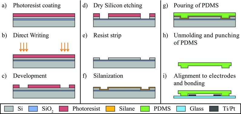
A PDMS mold is fabricated with a process based on silicon etching starting with either a silicon or a Silicon-On-Insulator (SOI) wafer. The use of a Si mold was first envisioned but was ruled out as explained in Sec. II A 2. We describe in Fig. 1 the full process starting with a SOI wafer.
FIG. 1.
Process flow for the PDMS mold fabrication (a) to (f), PDMS molding (g) and (h) and alignment with the glass chip (i).
A SOI wafer [handle wafer Si (thickness 380 μm)—buried oxide (thickness 2 μm)—device wafer Si (thickness 50 μm)] is coated with 2 μm of AZ1512 photoresist with the ACS 200 coater [Fig. 1(a)]. The photoresist is later patterned with the MLA 150 [Fig. 1(b)] (with a design scaled of 1.015 to compensate the PDMS shrinkage) and further developed with the ACS 200 [Fig. 1(c)]. The top silicon is etched with the Bosch process until the oxide layer is reached (with the Adixen AMS200 Deep Reactive Ion Etching (DRIE) etcher from Alcatel Micro Machining Systems, Annecy—France) [Fig. 1(d)]. The resist is then stripped from the wafer [Fig. 1(e)], which is later silanized with Trichloro(1H,1H,2H,2H-perfluorooctyl)silane (PFOTS from Sigma Aldricht) [Fig. 1(f)]. PDMS is later poured on the wafer [Fig. 1(g)], cured at 80 °C for 2 h before demolding, separating the PDMS slabs, and punching the access holes [Fig. 1(h)].
The last step which needs to be performed is the alignment between the PDMS slab and the glass chip patterned with electrodes [Fig. 1(i)].
2. Mold fabrication
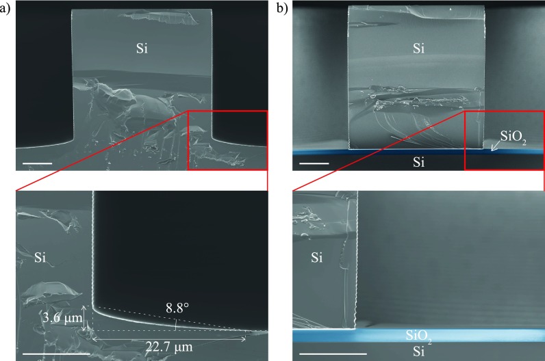
First trials of PDMS molding using an etched Si mold showed that PDMS walls did not bond completely up to the edge. This issue was further explained by Scanning Electron Microscope (SEM) pictures which showed that the edge of the Si mold structure had a different etched depth as presented in Fig. 2(a). To overcome this issue, a SOI wafer was used so as to stop the etching as soon as the oxide would be reached, allowing to obtain a right angle in the mold structure as presented in Fig. 2(b).
FIG. 2.
Scanning Electron Microscope (SEM) images of (a) a Si mold and (b) a SOI mold. For the sake of clarity, the oxide layer is artificially colored in blue. Scalebar 10 μm.
3. PDMS molding in PMMA sarcophagus
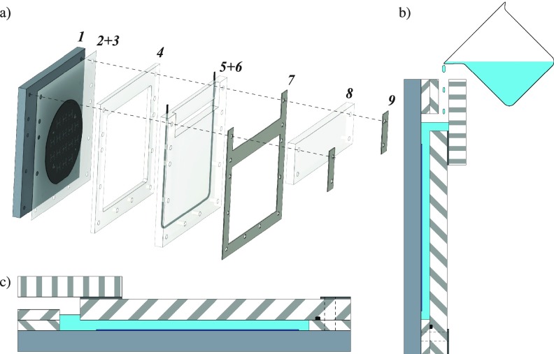
To obtain a specific and reproducible thickness of PDMS and perfectly parallel surfaces, a PMMA sarcophagus mold was used as shown in Fig. 3(a). This mold is composed of a 10-mm-thick aluminum part with threaded holes for the support (1). The wafer mold (3) is fixed with UV sensitive tape (2) to a PMMA part (4) defining the thickness of the PDMS. The PMMA cover (6) imposes the top surface of the PDMS to be flat and parallel and the combination with the closing PMMA part (8) enables a vertical pouring of the PDMS [Fig. 3(b)] as well as a horizontal position for PDMS curing [Fig. 3(c)]. The gasket (5) located in a groove of the PMMA part (6) enables the sealing for both PDMS and air during degassing. The inox parts (7) and (9) are here to homogenize the stress distribution in the PMMA pieces (6) and (8).
FIG. 3.
(a) Exploded view of the sarcophagus for PDMS molding. (b) Cross-section of the sarcophagus during PDMS pouring. (c) Cross-section of the sarcophagus in curing position.
A 10:1 mix ratio (base/curing agent) of PDMS (Sylgard 184 from Dow Corning) is poured in the sarcophagus mold and further degassed in a desiccator. The sarcophagus mold is then placed horizontally in the oven for 2 h. Exposure of the UV sensitive tape to UV light after PDMS curing enables to retrieve the wafer mold after each molding. PDMS retrieval is described in the supplementary material (Unmolding of PDMS and following). The different PDMS slabs are then separated and access holes are punched.
Here, the PDMS shrinkage (Sylgard 184 from Dow Corning) was characterized in the sarcophagus mold after curing at 80 °C for 2 hours with a 10:1 mix ratio (base/curing agent). We obtained a scaling factor of 1.015 corresponding to the shrinkage of 1.5% measured on a 1 cm distance, which is in good agreement with previously reported values.20,32
A detail procedure of the sarcophagus mold assembly and final PDMS retrieval is provided in the supplementary material, together with all the CAD files and drawings.
B. Alignment
1. Alignment with mask Aligner
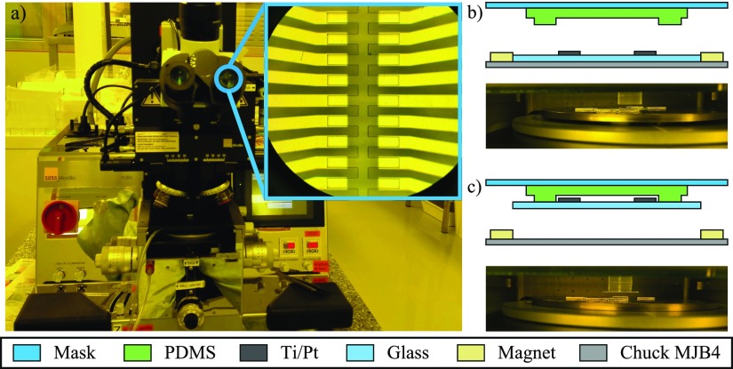
The alignment is based on a conventional mask aligner MJB4 (SUSS MicroTec—Garching, Germany) [Fig. 4(a)]. A custom-made steel chuck is used, covered with a 10 μm layer of nickel deposited by chemical nickel plating to prevent rusting (see Fig. S1 in the supplementary material). The lateral positioning of the glass chip is ensured by magnets which means that any chip smaller than 4 in. can be positioned with the magnets and the vacuum is no longer required.
FIG. 4.
(a) MJB4 mask aligner used in the alignment procedure and eyepiece view (inset). (b) Scheme (cut view) and picture of the PDMS and chip before contact and (c) after plasma bonding.
The PDMS slab is positioned on the glass mask, with the microfluidic features side facing the custom-made chuck for the pre-alignment. After plasma treatment, the PDMS slab is aligned with the glass chip using alignment marks [Fig. 4(b)]. Once the rotation angle and the X and Y positions are corrected, the chuck is moved up until the contact. The chuck is then moved down leaving the bonded assembly PDMS-glass chip in contact with the glass mask [Fig. 4(c)]. The bonded chip is carefully removed from the glass mask using tweezers and then placed in the oven at 80 °C with a 40 g weight on top of it for 10 min.
A detail procedure of the alignment with the MJB4 mask aligner is provided in the supplementary material, together with the CAD files and drawings of the custom-made chuck.
2. Results and discussion
The aligned chip is displayed in Fig. 5(a) and the alignment, illustrated in Fig. 5(b), is quantified using an image made by means of an optical microscope. The MJB4 mask aligner has a Top Side Alignment (TSA) accuracy of less than 0.5 μm. The typical misalignment is less than 1 μm over 3 mm distance which is mostly due to the shrinkage of PDMS corresponding to a resolution of more than 10 μm/cm. The medium misalignment was found to be 0.4 μm with a sample standard deviation of 0.2 μm. The estimation error of the misalignment was in the order of 0.3 μm (cf. supplementary material for more details). To make the design more tolerant to misalignment, the microfluidic channels used are 50 μm wide and the electrodes 60 μm wide. Since the glass is 700 μm thick, long distance objectives (20× and 40×) have been used but a more precise characterization is limited by the thickness of the glass. To reduce the misalignment, the shrinkage characterization can be more precise and performed on a larger area like the wafer scale.
FIG. 5.
(a) Fabricated chip with the PDMS slab bonded on the glass chip patterned with electrodes. (b) Zoom in the DEP focusing region of the chip with an optical microscope. The channel was filled with a blue dye to make sure that there was no leak. Scalebar 50 μm.
The global thickness of the PDMS slab + glass chip should not exceed 6 mm to keep the vacuum clamping of the glass mask when the Wedge Error Compensation (WEC) knob is lowered down. If thicker PDMS should be used, then the mask (standard thickness 2.3 mm) or the chuck (custom-made chuck thickness 3 mm) should be thinner.
No leakage was noticed on the chip, neither locally as proved by Fig. 5(b) nor globally as shown by Fig. S1 of the supplementary material.
III. CONCLUSION
In this paper, we have shown a reproducible method for μm precision alignment of PDMS microchannels with coplanar electrodes using a mask aligner, which is now routinely used to fabricate chips in the lab. This method relies on both PDMS molding with a PMMA sarcophagus for precise thickness and parallelism between the PDMS surfaces, and the use of a mask aligner with a custom-made chuck. This technique can also be used for PDMS-PDMS alignment, providing a high accuracy.
IV. SUPPLEMENTARY MATERIAL
See supplementary material for the full sarcophagus CAD parts and drawings and mounting procedure, the full alignment procedure and the custom-made MJB4 chuck CAD and drawings. The misalignment characterization procedure is also presented with the related measurements.
ACKNOWLEDGMENTS
The authors would like to thank the CMi staff at EPFL for their precious advice and the technical assistance. The authors would also like to thank the Atelier de l'Institut de Microtechnique (ATPR) at EPFL for their advice in the conception of the sarcophagus and the production of the sarcophagus pieces and the custom-made steel chuck. Ampere lab would like to acknowledge support from INSERM (Plan Cancer, Physicancer Program, Dynamo project). The authors also acknowledge the support of the mobility program of the Programme Avenir Lyon Saint-Etienne (PALSE).
References
- 1. Zhou J., Ellis A. V., and Voelcker N. H., Electrophoresis 31(1), 2–16 (2010). 10.1002/elps.200900475 [DOI] [PubMed] [Google Scholar]
- 2. Lotters J. C., Olthuis W., Veltink P. H., and Bergveld P., J. Micromech. Microeng. 7(3), 145–147 (1997). 10.1088/0960-1317/7/3/017 [DOI] [Google Scholar]
- 3. Bhagat A. A. S., Jothimuthu P., and Papautsky I., paper presented at the TRANSDUCERS 2007—International Solid-State Sensors, Actuators and Microsystems Conference ( IEEE, 2007) 10.1109/SENSOR.2007.4300186. [DOI] [Google Scholar]
- 4. Huh D., Matthews B. D., Mammoto A., Montoya-Zavala M., Hsin H. Y., and Ingber D. E., Science 328(5986), 1662–1668 (2010). 10.1126/science.1188302 [DOI] [PMC free article] [PubMed] [Google Scholar]
- 5. Moreira N. H., de Almeida A. L., Piazzeta M. H., de Jesus D. P., Deblire A., Gobbi A. L., and da Silva J. A., Lab Chip 9(1), 115–121 (2009). 10.1039/B807409G [DOI] [PubMed] [Google Scholar]
- 6. Kim R., Joo S., Jung H., Hong N., and Nam Y., Biomed. Eng. Lett. 4(2), 129–141 (2014). 10.1007/s13534-014-0130-6 [DOI] [Google Scholar]
- 7. Shi J. J., Huang H., Stratton Z., Huang Y. P., and Huang T. J., Lab Chip 9(23), 3354–3359 (2009). 10.1039/b915113c [DOI] [PubMed] [Google Scholar]
- 8. Doh I. and Cho Y. H., Sens. Actuator, A 121(1), 59–65 (2005). 10.1016/j.sna.2005.01.030 [DOI] [Google Scholar]
- 9. Holcomb R. E., Kraly J. R., and Henry C. S., Analyst 134(3), 486–492 (2009). 10.1039/B816289A [DOI] [PubMed] [Google Scholar]
- 10. Demierre N., Braschler T., Muller R., and Renaud P., Sensor Actuator, B 132(2), 388–396 (2008). 10.1016/j.snb.2007.09.078 [DOI] [Google Scholar]
- 11. Zhu Z., Chen P., Liu K. G., and Escobedo C., Micromachines-Basel 7(12), 230 (2016). 10.3390/mi7120230 [DOI] [PMC free article] [PubMed] [Google Scholar]
- 12. Zhang Z. Y., Zhao P., Xiao G. Z., Watts B. R., and Xu C. Q., Biomicrofluidics 5(4), 046503 (2011) 10.1063/1.3659016. [DOI] [PMC free article] [PubMed] [Google Scholar]
- 13. Ren Y. F., Huang S. H., Mosser S., Heuschkel M. O., Bertsch A., Fraering P. C., Chen J. J. J., and Renaud P., Micromachines-Basel 6(12), 1923–1934 (2015). 10.3390/mi6121465 [DOI] [Google Scholar]
- 14. Menad S., El-Gaddar A., Haddour N., Toru S., Brun M., Buret F., and Frenea-Robin M., Langmuir 30(19), 5686–5693 (2014). 10.1021/la5005193 [DOI] [PubMed] [Google Scholar]
- 15. Adler S. B., J. Electrochem. Soc. 149(5), E166–E172 (2002). 10.1149/1.1467368 [DOI] [Google Scholar]
- 16. Choonee K. and Syms R. R. A., J. Micromech. Microeng. 21(8), 085013 (2011). 10.1088/0960-1317/21/8/085013 [DOI] [Google Scholar]
- 17. Badshah M. A., Jang H., Kim Y. K., Kim T. H., and Kim S. M., J. Micro-Nanolithogr., MEMS, MOEMS 13(3), 033006 (2014). 10.1117/1.JMM.13.3.033006 [DOI] [Google Scholar]
- 18. Ye X. D., Liu H. Z., Ding Y. C., Li H. S., and Lu B. H., Microelectron. Eng. 86(3), 310–313 (2009). 10.1016/j.mee.2008.10.011 [DOI] [Google Scholar]
- 19. Moraes C., Sun Y., and Simmons C. A., J. Micromech. Microeng. 19(6), 065015 (2009). 10.1088/0960-1317/19/6/065015 [DOI] [Google Scholar]
- 20. Lee S. W. and Lee S. S., Microsyst. Technol. 14(2), 205–208 (2008). 10.1007/s00542-007-0417-y [DOI] [Google Scholar]
- 21. Li J., Le Gac S., and Berg P. d i A v d., paper presented at the Eleventh International Conference on Miniaturized Systems for Chemistry and Life Sciences—the Proceedings of microTAS 2007 Conference, San Diego (2007), see http://doc.utwente.nl/62037/. [Google Scholar]
- 22. Land K. J., Mbanjwa M. B., Govindasamy K., and Korvink J. G., Biomicrofluidics 5(3), 36502–365026 (2011). 10.1063/1.3641859 [DOI] [PMC free article] [PubMed] [Google Scholar]
- 23. Huh D., Kim H. J., Fraser J. P., Shea D. E., Khan M., Bahinski A., Hamilton G. A., and Ingber D. E., Nat. Protoc. 8(11), 2135–2157 (2013). 10.1038/nprot.2013.137 [DOI] [PubMed] [Google Scholar]
- 24. Kim J. Y., Baek J. Y., Lee K. A., and Lee S. H., Sens. Actuator, A 119(2), 593–598 (2005). 10.1016/j.sna.2004.09.023 [DOI] [Google Scholar]
- 25. Chen A. and Pan T., Biomicrofluidics 5(4), 46505–465059 (2011). 10.1063/1.3670368 [DOI] [PMC free article] [PubMed] [Google Scholar]
- 26. Sivakumarasamy R., Nishiguchi K., Fujiwara A., Vuillaume D., and Clément N., Anal. Methods 6(1), 97–101 (2014). 10.1039/C3AY41618F [DOI] [Google Scholar]
- 27. Punniyakoti S., Sivakumarasamy R., Vaurette F., Joseph P., Nishiguchi K., Fujiwara A., and Clement N., Adv. Mater. Interfaces 4(7), 1601155 (2017). 10.1002/admi.201601155 [DOI] [Google Scholar]
- 28. Li X., Yu Z. T., Geraldo D., Weng S., Alve N., Dun W., Kini A., Patel K., Shu R., Zhang F., Li G., Jin Q., and Fu J., Rev. Sci. Instrum. 86(7), 075008 (2015). 10.1063/1.4927197 [DOI] [PMC free article] [PubMed] [Google Scholar]
- 29. Kipper S., Frolov L., Guy O., Pellach M., Glick Y., Malichi A., Knisbacher B. A., Barbiro E., Avrahami M. D., Yavets-Chen Y., Levanon E. Y., and Gerber D., Lab Chip 17(3), 557–566 (2017). 10.1039/C6LC01534D [DOI] [PubMed] [Google Scholar]
- 30. Demierre N., Braschler T., Linderholm P., Seger U., van Lintel H., and Renaud P., Lab Chip 7(3), 355–365 (2007). 10.1039/B612866A [DOI] [PubMed] [Google Scholar]
- 31. Shaker M., Colella L., Caselli F., Bisegna P., and Renaud P., Lab Chip 14(14), 2548–2555 (2014). 10.1039/c4lc00221k [DOI] [PubMed] [Google Scholar]
- 32. Marcus J. S., Anderson W. F., and Quake S. R., Anal. Chem. 78(9), 3084–3089 (2006). 10.1021/ac0519460 [DOI] [PubMed] [Google Scholar]
Associated Data
This section collects any data citations, data availability statements, or supplementary materials included in this article.
Supplementary Materials
See supplementary material for the full sarcophagus CAD parts and drawings and mounting procedure, the full alignment procedure and the custom-made MJB4 chuck CAD and drawings. The misalignment characterization procedure is also presented with the related measurements.


