Abstract
Inductive sensor-based measurement techniques are useful for a wide range of biomedical applications. However, optimizing the noise performance of these sensors is challenging at broadband frequencies, owing to the frequency-dependent reactance of the sensor. In this work, we describe the fundamental limits of noise performance and bandwidth for these sensors in combination with a low-noise amplifier. We also present three equivalent methods of noise matching to inductive sensors using transformer-like network topologies. Finally, we apply these techniques to improve the noise performance in magnetic particle imaging, a new molecular imaging modality with excellent detection sensitivity. Using a custom noise-matched amplifier, we experimentally demonstrate an 11-fold improvement in noise performance in a small animal magnetic particle imaging scanner.
Index Terms: Biomedical imaging, broadband noise matching, inductive sensors, low-noise preamplifier, magnetic particle imaging (MPI), transformer networks
I. Introduction
Broadband inductive sensing systems remain crucially important for biomedical applications ranging from medical imaging to wireless medical implants. Because such sensing systems often measure minuscule signal levels in the body, maximizing their signal-noise ratio (SNR) and detection sensitivity is a crucial part of system design. It is often necessary to use both ultra low-noise amplifiers (LNAs) to amplify these signals and various noise-matching techniques to further improve the overall system SNR. However, for inductive and capacitive-based signals occupying large bandwidths, optimal noise-matching to LNAs can be particularly challenging due to the frequency dependence of the sensor reactance.
Here we describe optimal broadband noise-matching using ideal and transformer-like networks for inductive sensors and apply an optimal transformer-like matching network to inductive detector coils used in Magnetic Particle Imaging (MPI), an emerging tracer-based medical imaging technique [1], [2]. MPI directly images the intense nonlinear Langevin magnetization of superparamagnetic iron oxide (SPIO) tracers for high image contrast with no background tissue signal. MPI has already demonstrated robust systemic tracking of SPIO-labeled stem cells in the body with a detection limit of < 200 cells [3], [4]. Indeed, the detection sensitivity of MPI may soon approach that of nuclear medicine techniques, making it useful for future clinical applications in cancer imaging, stroke diagnosis and staging, and cell therapy tracking [5], [6].
MPI detector coils operate in the considerably broadband 20 kHz to 1 MHz regime (Very-Low Frequency to Medium Frequency). In this regime, the reactance of such detector coils can change by well over 30 dB, making noise-matching over that bandwidth especially challenging.
In this work, we first describe theoretical fundamental trade-offs between noise performance and bandwidth for inductive sensors. We then present a method to optimize noise-matched bandwidth using networks with transformers and transformer-like elements. Finally, we present a custom noise-matched preamplifier network that enables a bandwidth-optimized 3-dB noise figure for the MPI detector system in a 7 T/m 3D small-animal MPI scanner. The techniques and theory presented here are widely applicable to other measurement systems using inductive sensors, such as low-field Magnetic Resonance Imaging (MRI), implantable monitoring, and other wireless telemetry devices.
II. Theory
A. Noise in Inductive Sensors
The modeling of electronic noise in low-level voltage sensor-based detector systems has been extensively studied and described in detail [7]–[13]. We briefly summarize these concepts and relevant terms in Appendix A.
An equivalent noise circuit model for induction-based signal detection systems like MPI is shown in Fig. 1, where L is the inductance of the detector coil, and RL is the detector coil resistance [1], [2], [14]–[16]. We note that at the MPI frequency regime, patient-induced noise can be far lower than that arising from the detector coil for current scanner designs [17], [18] and will not be considered in this work.
Fig. 1.

Circuit noise model for inductive sensors and summary of noise-matching techniques using transformer-like matching networks. The source impedance is comprised of the coil resistance RL and inductance L. The equivalent voltage and current noise of the preamplifier are and , respectively. To reduce the apparent voltage noise contribution from the preamplifier, it is possible to increase the number of turns in the MPI detector coil by Nt-fold, the number of parallel amplifier devices by Np-fold, or through the addition of a 1:Nx input transformer. We show Nt, Np, and Nx have equivalent effects on system noise factor (F) and bandwidth, and can be combined into an equivalent noise-matching factor N (Appendix B). However, these noise-matching techniques may alter the input-referred input impedance Zin, which may affect output loading and the detector-amplifier LC resonance.
We begin with the noise factor (F) equation for inductive receivers:
| (1) |
| (2) |
where ω/2π is the frequency in Hz. Typical resistance values for MPI detector coils range from 0.1 to 10 ω, which corresponds to a thermal noise voltage between 40 and 400 . As an example, without noise-matching, the noise factor (F) of a Stanford Research Systems SR560 low-noise preamplifier (4 ), with a 500 μH, 5Ω MPI detector coil (290 ), is exceptionally poor at 23 dB.
B. Fundamental Noise-Matching Bandwidth Limits for Inductive Sensors
Bode and others have shown that there exists a fundamental tradeoff between impedance-matched bandwidth and the quality of the match to reactive sources and loads [19]–[22]. Fano [20] derived for serial inductors (as in Fig. 2(a)), assuming large Q-factors, that for a desired impedance match with reflection coefficient Γ (ω):
| (3) |
where Zrhp are the right-half plane zeros of Γ (ω). Eq. (3) shows an upper limit to the matched bandwidth. Systems with a larger tolerance for in-band mismatches, and hence larger in-band reflection coefficients, have a smaller integrand and therefore can be matched to a broader bandwidth. The reflection coefficient Γ (ω) is defined:
| (4) |
where ZL is the source impedance and Ro is the resistive load to be matched. For the noise-matching problem at hand, we substitute Ro with equivalent noise resistance of the LNA, which is defined as , or the optimally matched noise resistance derived in Appendix A (Eq. (23), see Fig. 2). The F equation can then be expressed in terms of the reflection coefficient:
| (5) |
| (6) |
| (7) |
| (8) |
Fig. 2.
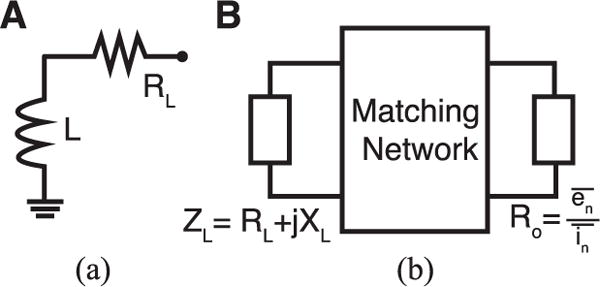
(a) Serial inductive source or load in analysis. (b) Diagram of general noise-matching networks to reactive sources. XL is the source reactance.
In the ideal impedance matching case [20], |Γ (ω)| is constant in the passband and 1 elsewhere to maximize matched bandwidth Δω = ω2 − ω1. Using Eq. (3), we can solve for this maximum ideal matched bandwidth:
| (9) |
| (10) |
This expression diverges for , as it is not possible to achieve a F smaller than the limit given in Eq. (23), which is itself only achievable at one frequency for a reactive source. However, for any , the logarithm in the denominator can be simplified using the Taylor series expansion:
| (11) |
Using the positivity of the Taylor expansion terms at 0 ≤ x < 1 to relax the inequality in Eq. (10), we find the maximum ideal noise-matched bandwidth as a function of the desired F, source impedance, and amplifier characteristics:
| (12) |
Hence a fundamental direct trade-off exists between the achieved F and noise-matched bandwidth, a phenomenon also previously observed for Magnetic Resonance Imaging coils [23]. We note that the first-order Taylor series approximation relaxes the inequality in Eq. (10) by less than 10% error for values of , less than 50% error for values of , and by π RL/L as the desired F approaches the noise-matching limit in Eq. (23). In all cases, the noise-matched bandwidth can be improved by using LNAs with low product, such as ultra low current-noise field-effect transistors (FETs). However, while it appears arbitrary lowering of the sensor quality-factor (Q) or increasing the sensor temperature would also improve noise-matching quality, such approaches may only increase sensor noise and thereby degrade overall system SNR [24].
C. Optimal Noise-Matching to Inductive Sensors via Transformer-Like Networks
A wide variety of low-loss circuit network topologies are available for impedance and noise matching [22]. The transformer-coupled network is one of the most common matching topologies and introduces minimum signal phase shifts compared to more complicated multi-stage networks. In Appendix B, we present three transformer-like methods for noise matching and demonstrate their equivalent effects on the overall system SNR. These methods include increasing the number of turns in the inductive detector, using parallel LNA devices, and adding an input matching transformer before the LNA. A diagram of all three techniques is shown in Fig. 1.
Combining the F modifications enabled by each matching technique (Eqs. (32), (37), and (41)) yields:
| (13) |
where we introduce N, the equivalent noise-matching ratio formed by combining all three techniques, as . Nt is the ratio by which the number of turns in the detector coil can be increased, Np is the number of parallel LNA devices, and Nx is the primary to secondary turns ratio of an input matching transformer.
The use of these matching techniques may also influence other system behaviors. For example, it may be desirable to avoid resonant effects between inductive sensors and the LNA input capacitance. In MPI, such resonances could cause amplitude and phase shifts in the signal spectrum and make robust image reconstruction challenging [2], [25]. Assuming low detector self-capacitance, this resonant frequency can be written:
| (14) |
where Cin is the input capacitance of the LNA. The use of the transformer-like matching techniques presented in Appendix B lowers the sensor’s resonant frequency (combining Eqs. (33), (38), and (42)):
| (15) |
Further, the noise-matching factor N must be chosen carefully due to the inherent trade-off in F and noise-matched bandwidth. Below we analyze this trade-off for transformer-coupled networks. We begin with Eq. (13) and a given F (assuming large detector coil Q, or ωL ≫ RL):
| (16) |
| (17) |
Equation (17) is a quadratic function of N in the form aN2 + bN + c = 0, where , b = − (F – 1) · 4kbTRL and . To find the maximum realizable bandwidth for a given F, we solve for the real roots of Eq. (17). A real-valued solution for N requires that b2 ≥ 4ac:
| (18) |
| (19) |
Again, the noise-matched bandwidth is shown to trade off directly with desired F. However, the transformer-like matching network is less efficient than the ideal case given in Eq. (10), in that |Γ (ω)| is non-constant in the passband and non-zero in the stopband. As a result, the maximum noise-matched bandwidth achievable using a transformer-coupled network is π times lower than the ideal bandwidth derived in Eq. (12). We note here the implicit assumption that RL is not significantly frequency-dependent, which holds true with the proper design and use of stranded litz wire at sufficiently low frequencies [26].
One consequence of Eq. (17) is that the values of the noise-matching factor N depend on the desired maximum bandwidth ω. For any ω less than the right-hand expression in Eq. (19), then b2 > 4ac and hence there must exist two real-valued noise-matching factor N which can achieve the desired ω. Moreover, from Eq. (19) we see that for the roots of N to be real-valued, the maximum ω achievable is when Eq. (19) becomes an equality, which results in an optimal .
In summary, for the class of inductor-based sensors, we have derived fundamental noise-matching limits and described a method for designing optimal transformer-like matching networks from a desired F metric. We have also presented three transformer-like matching methods for inductive sensors, which include changing the number of turns in the detector coil, paralleling active devices in the preamplifier, and adding the use of an input matching transformer. Below, we describe the design, implementation, and performance of a custom LNA and transformer-coupled noise matching network for a small-animal MPI imager.
III. Methods
A. Design of a Noise-Matched MPI Preamplifier
The prototype solenoidal detector coil in an existing 7 T/m small-animal MPI scanner has an inductance of approximately 500 μH and an AC resistance of approximately 5 Ω in the MPI band up to 1 MHz, which has a thermal noise voltage of 290 .
We began by choosing a device with low input noise that can achieve high signal bandwidth. Two figures of merit were used in selecting an appropriate amplifier device. First, the product gives an excellent metric for the lowest achievable NF (Eq. (23)) and noise-matched bandwidth (Eq. (19)). Second, the expression is useful for evaluating the effect on the LC resonant frequency between the coil inductance and the preamplifier input capacitance due to noise-matching. A similar figure of merit for LNAs selection is discussed in [13].
Based on these figures of merit, we chose the low-noise ADA4817 JFET operational amplifier from Analog Devices, which has at 2.5 and Cin at 1.3 pF. 1/f noise for this device occurs mainly at frequencies below 10 kHz. From 10 kHz onward the voltage noise is rated at less than 5 ; from 100 kHz onward it is below 4 .
Solving Eq. (19) for this amplifier and detector coil combination yields a maximum achievable 3 dB noise-matched bandwidth at 1.3 MHz for a noise-matching factor N of 386. Using this noise-matching factor, the resonant frequency between the detector coil and the noise-matched amplifier input is around 317 kHz (Eq. (15)) in the absence of parasitic impedances. Fig. 3 shows system noise figure scaling with other values of the noise-matching factor N for the ADA4817 amplifier.
Fig. 3.
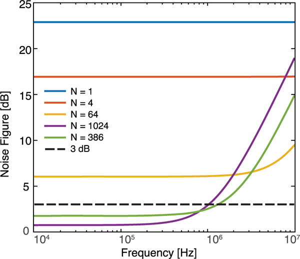
Calculated noise figure as a function of frequency and noise-matching factor N for the specified voltage and current noise characteristics of the ADA4817 operational amplifier. The maximum achievable bandwidth over which the system has a noise figure less than 3 dB is 1.3 MHz, which occurs at N = 386. Note: JFET flicker noise is not shown here, but the input voltage noise for the ADA4817 is less than 5 from 10 kHz onward. Correlated voltage-current noise is likewise not shown, but would degrade noise figure by no more than 30% (2.3 dB) at frequencies above 5 MHz [11], [13].
B. MPI Preamplifier Circuit Design
To increase N for matching, we used a two-stage LNA design using parallel ADA4817 devices (Fig. 4). The first stage incorporated 24 parallel noninverting-input amplifiers, which were averaged via a summing amplifier configuration in the second stage. The amplifier gain in the first stage was designed to be 21, and the gain-setting resistors on the negative input terminal were chosen at low resistance values to minimize thermal noise contribution to each OPA circuit. A serial input resistance was used to keep the OPA circuit stable on the low-capacitance printed circuit board and avoid crosstalk with other parallel amplifier devices. This 50 Ω serial input resistor has approximately 0.9 voltage noise, which, combined with the voltage noise from the feedback and gain resistors [27], increases the effective of each OPA circuit by only 0.11 from the rated 4 voltage noise. To compensate for differing offsets among the paralleled devices, we added serial output resistors for each device for better load current balancing and designed the circuit with a low gain (21) to allow for a higher tolerance in the output dynamic range [28].
Fig. 4.
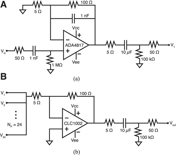
(a) A noninverting amplifier configuration is used for the LNA first stage of the MPI preamplifier. A 50–Ω input resistor is added for stability. (b) Inverting summing amplifier configuration for the second stage of the MPI preamplifier.
The summing amplifier was designed with the exceptionally-low CLC1002 BJT operational amplifier (Exar Corp., Fremont, CA), at 0.6 . The gain of the second amplifier stage was designed to be around 13.7, for a total system gain of 288. Accounting for noise in the serial input resistors and the gain-setting resistors, the overall calculated input-referred voltage noise of this preamplifier is 0.84 .
C. MPI Preamplifier Printed Circuit Board Layout and Input Transformer
A custom printed circuit board for the LNA was designed using Diptrace software (Novarm Ltd.). The board design incorporated five layers, with the top and bottom layers respectively used for input and output signals and the middle layers used as ground and power planes. To reduce stray input capacitance, copper planes from the ground and power planes underneath the input traces were removed as much as possible without compromising circuit stability [29]. The MPI preamplifier circuit board was manufactured by Bay Area Circuits, Inc. (Fremont, CA). LNA power at ±5 V was supplied via a custom board using low-noise, low-dropout voltage regulators from Texas Instruments (LM1085 and LM7905). Bypass capacitors with capacitance values 0.1, 1, and 10 μF were used to decouple noise at the positive and negative supply pins at each OPA device. A photograph of the constructed preamplifier is shown in Fig. 5.
Fig. 5.
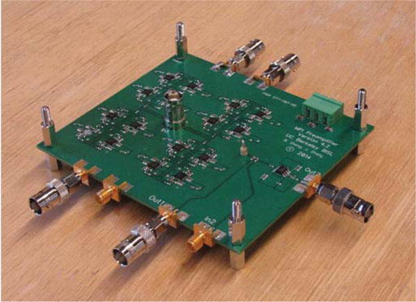
Constructed MPI preamplifier achieves a gain of 265 and input-referred voltage noise of 1.06 .
An input matching transformer was constructed using a toroidal core using Type 75 material from Fair-rite Products Corp, (Wallkill, NY), which has a permeability μr of 5000. The primary and secondary windings are constructed using 30 AWG wire using a turns ratio of 4.3, with respective inductances of 2.5 mH and 40 mH. The use of this 1:4.3 transformer with the 24 parallel-connected ADA4817 amplifiers gives an effective noise-matching factor N of 444, which is close to the calculated optimal value of 386. The primary winding resistance in the transformer was 0.5 Ω, which has of 90 . The secondary winding resistance was measured at 12 Ω. Together, the parasitic losses from the transformer windings are calculated to increase the total input-referred LNA noise from 250 to 280 , and thus would not significantly degrade noise figure [12].
IV. Results
In the following Section, we present the noise performance of the custom MPI preamplifier and demonstrate its use and imaging performance in the preclinical MPI scanner.
A. MPI Preamplifier Noise Specifications
Calculated and measured noise and input impedance characteristics for the constructed MPI preamplifier are shown in Table I and Fig. 6. Gain and input-referred voltage noise for the preamplifier match well with expected values at 265 and 1.06 , respectively, directly measured from 10 to 200 kHz using a commercial audio analyzer (SR1, Stanford Research Systems). The gain was measured using low-distortion, 1 mVrms input signals at 10, 20, 40, 80, 160, and 200 kHz and was consistent at 265 in this frequency range. Second and third-order harmonic distortion measurements of a 1 mVrms, 40 kHz sinusoid signal were found to be around −80 dB, which is comparable to that achieved by the commercial SR560 preamplifier and is satisfactory for MPI applications [4]. The total input capacitance was found to be around twice the expected input capacitance of 24 parallel ADA4817 devices alone, suggesting that parasitic capacitance in the circuit board was around 32 pF. This parasitic capacitance is likely due to the large surface area between the input signal traces to all 24 LNA devices and the board’s supply and ground planes, and may be improvable via improved board layout and the use of guard ring buffers on device inputs [28].
TABLE I.
Measured and theoretical gain and noise properties of noise-matched preamplifier
| LNA
|
LNA-Transformer
|
||||
|---|---|---|---|---|---|
| Theory | Data | Theory | Data | ||
| Gain | 288 | 265 | 1237 | 1150 | |
|
|
0.84 | 1.06 | 0.25 | 0.28 | |
| Cin (pF) | 31.2 | 63.2 | 577 | 1300 | |
Fig. 6.
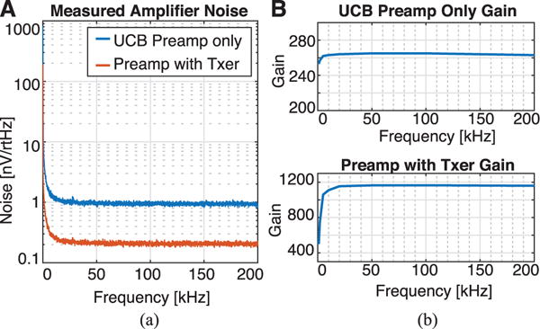
Measured noise and gain characteristics for UCB preamp. (a) Input-referred noise measurements showed 1.06 and 0.28 noise respectively for the bare MPI preamplifier and the transformer-coupled preamplifier from 10–200 kHz. Measurements were performed using an SR1 audio analyzer with shorted LNA inputs. (b) Measurements of LNA gain showed gains of 265 and 1150 from 10 kHz to 200 kHz, respectively, for the bare and transformer-coupled preamplifiers. Measurements were performed using an SR1 audio analyzer with 1 mVrms inputs.
The addition of a 1:4.3 input transformer in the detector system increases the total signal gain to 1150 (from 10 kHz to 200 kHz using the same parameters as above), which matches the expected gain. The transformer also reduces the effective amplifier voltage noise down to around 280 from 10 kHz to 200 kHz as expected, which is equivalent to the thermal noise in a 5 Ω resistor. Finally, the input capacitance of the transformer-coupled preamplifier system is increased by a factor of 4.32 to 1.3 nF, as expected. The resonant frequency between the noise-matched LNA with a 500 μH detector coil was determined to be close to 200 kHz, as determined using S-parameter analysis using a HP 4195A network analyzer.
To test the noise performance of the MPI LNA, we measured the thermal noise in resistors ranging from 0.1 Ω to 1 k ω (Fig. 7). In these experiments, a resistor was connected in series with the preamplifier and the total system voltage noise density from 10 to 200 kHz was directly measured. Our experimental voltage noise measurements match well with theoretical predictions, as the total noise voltage is dominated by preamplifier at low source resistances and by resistive noise for high source resistance values. For the MPI preamplifier alone, the apparent crossover point between amplifier and source noise dominance occurs at around 70–80 Ω. For the transformer-coupled preamplifier, this transition point occurs at around 4–5 Ω as expected.
Fig. 7.
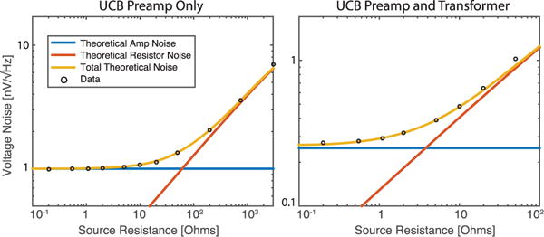
Measurements of input-referred thermal noise from 10 to 200 kHz for serial input resistances ranging from 0.1 Ω to 1 k ω are shown along with theoretical source resistor noise, amplifier voltage noise, and total input-referred noise for the custom MPI preamplifier alone and the preamplifier with transformer coupling. The measured noise-spectral density was frequency-independent in this bandwidth. Total input-referred noise measurements for varying resistor values correspond well with theory.
B. MPI Phantom Imaging Studies
We performed imaging studies in a preclinical MPI scanner to compare the imaging noise performance of the custom LNA to existing low-noise preamplifiers. The MPI scanner used was a custom 7 T/m gradient, field-free point small-animal MPI scanner [30] operating at 20.05 kHz drive field frequency and 40 mTpp drive field amplitude. The MPI scanner detector coil had an inductance of 470 μH and resistance of 5 Ω and was wound in a gradiometer configuration to suppress feedthrough interference from the drive coil. A 4-stage LC notch filter at 20.05 kHz was connected in series with the detector coil to further reduce feedthrough interference. The use of this notch filter did not affect MPI phase more than 0.45° at 2f0, which was found to be tolerable for image reconstruction. All MPI images were reconstructed using an x-space imaging reconstruction algorithm [2], [25] and were not postprocessed after image reconstruction. LNA devices used for MPI imaging included a SR560 commercial preamplifier from Stanford Research Systems with a gain of 200 and of 4 , an Exar CLC1002 noninverting amplifier with a gain of 24 and of 0.6 , and the custom tranformer-coupled MPI preamplifier here (Fig. 8).
Fig. 8.
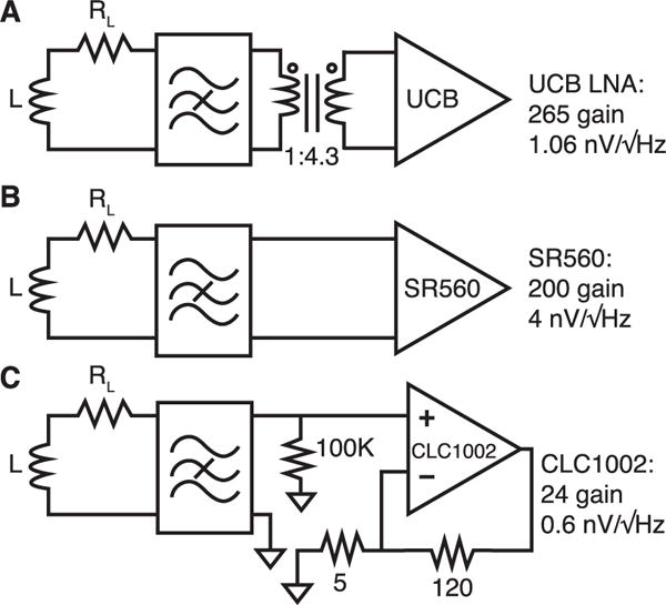
Experimental amplifiers used for MPI imaging. MPI signals from the detector coil (with L of 500 μH and RL of 5 Ω are filtered for direct feedthrough interference [25] using a custom notch filter prior to signal amplification using (a) Berkeley custom low-noise amplifier and transformer setup as presented in this work, (b) directly connected to an SR560 preamplifier with 200 gain, and (c) a noninverting amplifier using the CLC1002 op amp with gain around 24.
Phantom imaging studies used a custom-built sensitivity imaging phantom (Fig. 9). The phantom was machined from an extruded acrylic rod with 3.5 cm diameter. Six equidistant holes with 2 mm diameter and 7 mm depth were drilled into the phantom. 10 μL of diluted SPIO tracer (Nanomag-MIP, Micromod, Rostock, Germany) with iron content ranging from 2.1 to 12.7 μg was pipetted into the phantom and sealed before MPI imaging. MPI phantom scans used a field of view (FOV) of 5 × 3.75 × 5 cm and a total scan time of 5 minutes.
Fig. 9.
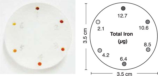
A ring-shaped acrylic MPI phantom with 10 μL of diluted SPIO tracer with iron content ranging from 2.1 to 12.7 μg.
MPI imaging results of the sensitivity imaging phantom are shown in Fig. 10. Images acquired using the custom MPI preamplifier show high SNR and are able to visualize all samples in the imaging volume. In contrast, the images acquired using the SR560 preamplifier show high image noise, especially at 40% of full image scale. Only 4–5 tracer samples are visually detectable in MPI images acquired using the SR560 preamplifier.
Fig. 10.
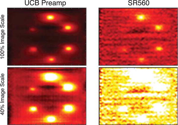
MPI imaging comparison using the custom transformer-coupled LNA and a commercial SR560 preamplifier. MPI images acquired using custom LNA shows significantly higher SNR than SR560. MPI imaging parameters: 5 × 3.75 × 5 cm imaging FOV, 5 minute scan time.
Image noise statistics from the MPI phantom imaging studies are shown in Fig. 11. To determine image noise, pixel values in the reconstructed MPI images were determined using regions of interest that contain no SPIO tracer. These image noise signals are then divided by the total detector system gain and normalized by the MPI bandwidth to determine equivalent input voltage noise density in . Using this method, we determined that the input-referred noise for the transformer-coupled MPI preamplifier to be 0.41 and 4.4 for the SR560, an 11-fold SNR improvement.
Fig. 11.
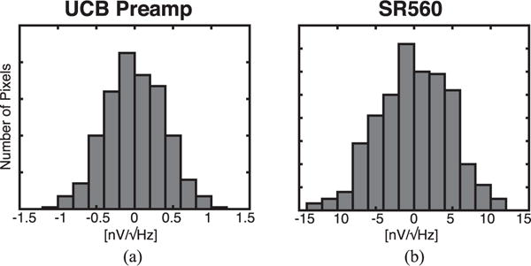
Image noise statistics from MPI phantom scans using the custom noise-matched LNA and SR560. To calculate image noise, pixel values in MPI images were determined using regions of interest (ROIs) that contain no SPIO tracer. The MPI image-derived noise standard deviation is 0.41 for the custom LNA and 4.4 for SR560.
The measured noise values match well with theory (Fig. 7), which predicts that the total input-referred noise for the custom LNA, which incorporates 0.29 thermal noise from the 5 Ω detector coil, is around 0.40 at frequencies below the noise-matched bandwidth (Eq. (19)). These data indicate that the custom MPI LNA, with 0.28 , has been noise-matched to below 3 dB.
Using the phantom images, we calculated the MPI imager’s sensitivity limit with these LNA devices by dividing the highest-concentration sample’s MPI signal by the standard deviation of the image noise. These results showed that the expected sensitivity limit, where the image SNR is equal to 1, for the SR560 is around 450 ng of iron tracer in a voxel. For the custom transformer-coupled MPI preamplifier, the sensitivity limit in this MPI scanner is as low as 50 ng of iron tracer.
C. MPI Animal Imaging Studies
Finally, we tested the MPI performance of the custom MPI LNA for rat liver imaging. Briefly, following a UC Berkeley-approved animal protocol, a 176 g, 5 month female Fischer 344 rat was intravenously injected using 1 mL of 1% Nanomag-MIP SPIO tracer. The animal was sacrificed 10 minutes following injection. MPI imaging was performed with 4 × 4 ×10 cm FOV and 457 second image acquisition using three LNA devices as described above. An X-ray image was acquired for image co-registration with 3 stitched FOVs and 30 kV, 800 μA power. X-ray acquisitions were 10 seconds each.
Fig. 12 shows MPI imaging results using each LNA device. As expected, images acquired using the custom noise-matched LNA showed significantly higher SNR than those acquired using the CLC1002 and SR560 amplifiers. Specifically, SPIO uptake in the liver and spleen can clearly be appreciated using the custom LNA device. These results are highly promising for future small-animal and clinical imaging applications that require high image sensitivity and SNR.
Fig. 12.
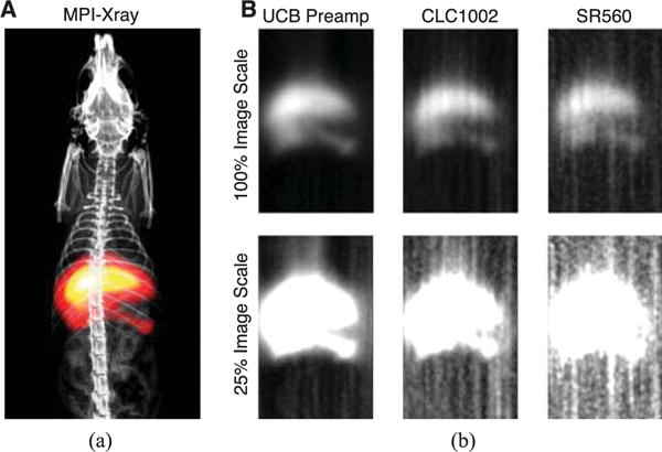
Comparison of MPI liver imaging using custom MPI LNA, CLC1002 op amp, and SR560 preamplifier. (a) Coregistered MPI and X-ray image of intravenous injections of SPIO tracer in rat, imaged using custom MPI LNA. (b) The custom LNA achieves significantly improved SNR performance compared to commercial amplifiers. MPI Imaging: 4 × 4 × 10 cm FOV, 7.6-min total acquisition. X-ray Imaging: three stitched FOVs, 30 kV, 800 μA, 10-s acquisition each.
V. Discussion
A. Optimal Matching Networks for Inductive Sensors
Here we presented a method to optimize transformer-like networks for impedance matching to inductive sources, enabling a 11-fold improvement in SNR for a small-animal Magnetic Particle Imaging scanner. The use of a transformer-like network was chosen here because it does not significantly affect signal amplitude and phase within the matched bandwidth. A wide array of other network topologies, such as familiar LC ladder networks, can be used as well. Using these networks, it is possible to achieve matching bandwidths and noise figures close to the optimum case in Eq. (12) with fewer than ten elements [22], for a π-fold improvement in noise-matched bandwidth over the transformer-like network. Proper design of these networks may also avoid additional noise, especially hard-to-measure current noise, potentially arising from the use of lossy transformers. The trade-off with such methods, however, is that any inductive matching elements may result in increased parasitic loss. Moreover, the frequency response of these matching networks must be carefully characterized and compensated during signal acquisition and reconstruction, especially for phase-sensitive broadband signal measurements like MPI.
B. Correlated Voltage and Current Noise in LNA Devices
In this work, we have assumed independent voltage and current noise generators for the derivation of optimal noise-matching parameters. For FET devices in practice, the voltage and current noise can be non-negligibly correlated at high frequencies, primarily due to channel thermal noise propagating through the gate-source capacitance [9], [11], [31], [32]. This adds an additional correlated current noise component with variance , with K1 a factor ranging from 0.25 or 0.3 [9], [32] to 0.67 [31]. This correlated noise term is strongly frequency-dependent and can dominate the shot noise in the gate leakage current at high frequencies. For our application, the thermal noise term was not taken into consideration, since it would dominate the rated 2 shot noise of the ADA4817 (with Cgs of 1.5 pF and gm around 19 mS) [33] only at 5 MHz and above. However, we anticipate this correlation term to be highly relevant for higher-frequency applications. For applications where the current noise would be fully correlated with the voltage noise, the voltage and current noise densities (not their variances) add directly [9]–[11]. In this case, the standard technique of directly adding voltage and current noise variances incurs a maximum error of 30% in calculating total amplifier noise [11], [13].
It must be noted that the LNA voltage and current noise sources are physically intrinsic to the device itself, and are not subject to voltage and current division by the source and amplifier input impedances. Hence, in our work we have simply assumed that intrinsic LNA noise is not modified by the source and input impedances. A more mathematically rigorous treatment of the two-port amplifier noise model is shown in [34, pp. 220–223], where the author constructs additional correlated voltage/current noise sources that make LNA noise mathematically invariant to the source and input impedance.
C. Matching Network Effects on LNA Input Impedance
We note that the noise-matching process is different from designing optimal power matching networks between the source impedance and the input impedance of the LNA device, which is wholly unrelated to its optimal equivalent noise resistance (Eq. (23)). However, the LNA input impedance (or, equivalently, the sensor source impedance) is also modified through noise-matching and may produce undesired effects on overall system performance. For example, in reducing the ratio, the transformer-like matching network presented here may also effectively reduce the LNA input impedance relative to the source, which may in turn produce undesired signal loading at the LNA. In MPI and other broadband sensor applications, one consequence of this effect is that an undesired resonance between the inductive sensor and the LNA input capacitance can be frequency-shifted into the signal-carrying bandwidth. In the present work, we observed a resonant frequency at around 200 kHz, significantly lower than the maximum noise-matched bandwidth at 1.3 MHz, owing to a combination of undesirable board capacitance and high matching factor N. Although this frequency still allowed for robust image reconstruction at up to ten harmonics of the drive field frequency, for higher-resolution MPI systems, future matching implementations may focus on reducing board parasitics and choosing an LNA device with a lower figure-of-merit. Thus it is important to compensate for these impedance-transformation effects in choosing an appropriate LNA device and in designing the matching network.
D. Detection Sensitivity in Current MPI Designs
Our results here indicate that using a noise-matched LNA enables an MPI detection sensitivity of less than 50 ng Fe for a 7 T/m field-free point scanner, an 11-fold improvement. This sensitivity limit can be further improved by the use of field-free line, projection-format MPI scanners [15]. An existing FFL MPI imager already demonstrated higher sensitivity at 5 ng detection limit in a voxel due to the more sensitive projection imaging format [3]. Hence, a combination of the noise-matching techniques presented here with the field-free line imaging format may improve detection sensitivity to well below 1 ng Fe per voxel.
E. Toward Patient-Noise Dominance in MPI
While body-noise dominance has already been achieved in MRI clinical scanners [17], it has so far proved elusive in MPI due to the low frequencies currently used. However, there are methods to improve thermal noise performance from MPI detector coils toward achieving body-noise dominance. First, the use of cryogenically cooled detector coils would decrease the thermal noise variance of the detector coil linearly with temperature. Liquid nitrogen cooling, for example, would reduce detector coil noise by two-fold over existing designs. Second, the overall MPI detector geometry can be changed to increase the total copper used in the construction of the detector coil for lower resistance. However, this method may incur trade-offs for the total bore space available in the MPI scanner. Third, non-traditional MPI scanning schemes at different frequency regimes may be used to further exploit the unique physics of the MPI tracer. Ultimately, a combination of these and other approaches may be needed to reach patient-noise dominance in clinical MPI scanners.
VI. Conclusion
In this work, we derived the fundamental limits of noise-matching performance and noise-matched bandwidth for inductive sensors, described three methods for noise matching using transformer-like networks, and demonstrated optimal transformer-coupled noise-matching to the detector coil of a custom 7 T/m small-animal MPI scanner. These noise-matching techniques are general principles and can be adapted to other reactive sensor systems. Using the constructed LNA, we demonstrated a 11-fold improvement in SNR performance for MPI scans over a commercial SR560 amplifier. The high SNR and sensitivity in MPI, enabled by these techniques, may make it highly useful for future clinical molecular imaging applications like cancer imaging, stroke diagnosis and staging, and cell therapy tracking.
Acknowledgments
The authors would like to thank Paul Keselman and Xinyi Zhou for animal assistance.
This work was supported by NIH 5R01EB013689, Keck Foundation Grant 034317, NIH 1R24MH106053-01, and NIH 1R01EB019458. The work of B. Zheng was supported by the Siebel Scholars program. This paper was recommended by Associate Editor J. Van der Spiegel.
Appendix A Noise in Electronic Measurement Systems
A theory of the noise performance of standard voltage measurement systems has been well established in the literature [7], [9]–[11]. Briefly, a noise model of a simple Thevenin-equivalent detector system is shown in Fig. 13 [7], [9]. The sources of electronic noise in such a system can be encapsulated in the thermal noise in the detector arising from its Thevenin resistance and the voltage and current noise of the preamplifier. In this work, we assume that all noise sources are uncorrelated, which is valid for most amplifier configurations [7], [9], [11]–[13] but not for certain amplifiers at high frequencies [35]. The total voltage noise variance of the system, in V2Hz−1, can then be expressed
| (20) |
where kb is Boltzmann’s constant, T is the temperature of the detector in Kelvin, Rs is the detector Thevenin resistance, is the amplifier voltage noise in , and is the amplifier current noise in .
Fig. 13.
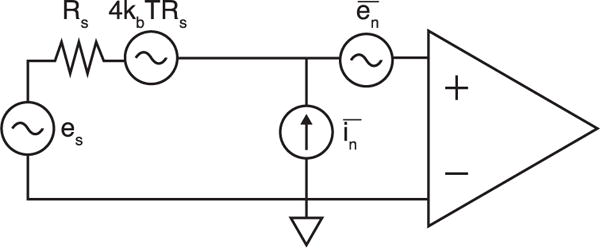
Generalized circuit noise model for voltage-based electronic measurement systems. The signal transducer model is shown as a Thevenin voltage source with signal es, where the sensor noise arises from the thermal noise of the source resistance (Rs). Electronic noise in the amplifier can be modeled using a serial voltage noise source with variance and parallel current noise source with variance .
A standard metric for characterizing noise performance is noise factor (F), which is defined as the SNR of the amplifier output divided by the SNR seen at its input, expressed either as a ratio or, in decibels, as noise figure. For the detector-amplifier systems described here, F is simply the relative ratio of the total input-referred noise in the system as compared to the detector noise alone. Notably, a noise figure below 3 dB implies that the total noise is dominated by thermal noise from the detector resistance and that the system is therefore ”noise-matched.” F can be expressed:
| (21) |
A differentiation of Equation (21) shows that F can be minimized when . At this detector resistance, the lowest achievable F is:
| (22) |
| (23) |
which is governed only by the amplifier’s voltage noise-current noise product and detector temperature. As a result, when choosing low-noise amplification devices, the amplifier noise power product @, and not their individual values, is the appropriate figure-of-merit to use for evaluating their lowest achievable noise performance.
Appendix B Noise-Matching Techniques for Inductive Sensors
Equivalent transformer-like methods to match the noise of inductive coils to a given amplifier device include changing the number of turns in the coil, paralleling the number of input amplifiers, and using a matching transformer [7], [24]. To understand their operation and equivalence, we begin by describing the signal generation mechanism in inductive sensors. Assuming that the geometry of the MPI detector coil is static, then according to the principle of reciprocity [36], the voltage signal generated in inductive sensors is:
| (24) |
where B1 is the sensitivity of the detector coil (or, equivalently, the field that is generated by the coil per unit current in T/A) and m is the detected magnetization signal.
The overall SNR of the MPI detector system can then be expressed in relation to the coil sensitivity and the total system noise:
| (25) |
| (26) |
1) Number of Turns in the MPI Detector Coil
One technique for noise-matching to inductive sensors is through changing the number of turns in the sensor coil, Nt [7]. From Ampere’s law, the magnetic field generated per unit current of such a coil, and therefore its B1 sensitivity, scales linearly with the number of turns, i.e., B1 ∝ Nt. The inductance of the detector coil scales quadratically with the number of its turns, [37].
In practice, the detector coil geometry is limited, which trades off the number of turns with the cross-sectional area of each turn. Hence, for an example solenoidal coil with fixed length Lc, thickness Wc, and average radius Rc, the resistance of the detector coil windings can be expressed:
| (27) |
| (28) |
| (29) |
where Lw is the length of wire used in the coil, Aw is the cross-sectional area per turn, ρ is the resistivity of the coil, and A is the total coil cross-sectional area. As the number of turns increases, the cross-sectional area per turn decreases and the total wire length increases, resulting in a quadratic increase in resistance. It is important to note that these calculations assume that the AC resistance of the windings is not significantly frequency-dependent, i.e., the skin effect and proximity effect are accounted for via the use of appropriately stranded litz wire at sufficiently low frequencies. As an example, the AC resistance at 1 MHz of transformer windings constructed using 48 AWG stranded litz wire is only approximately 1.3-fold higher than its DC resistance, making the assumption suitable for MPI bandwidths [26].
Hence, if we increase the number of turns in the detector coil by a factor of Nt, then the SNR equation becomes:
| (30) |
| (31) |
Equivalently, F becomes:
| (32) |
Although Eq. (32) shows that the apparent preamplifier voltage noise has decreased by a factor of Nt and the current noise has increased by Nt, it is important to note here that the SNR is modified only by the increase in coil sensitivity, the thermal noise in the coil, and current noise through the modified coil reactance.
Increasing the number of turns in the detector coil also shifts the resonant frequency between the detector coil and the preamplifier capacitance:
| (33) |
Caution must be exercised in using this technique: excessively increasing the number of turns in the detector coil will both induce additional losses due to the proximity effect and may undesirably lower the self-resonant frequency into the signal bandwidth.
2) Parallel LNA Devices
Another method to improve the F for MPI detector systems is to place multiple amplification devices in parallel [8], [13], [16], [24], [38]. In this method, the detector coil is connected to the parallel-connected input of multiple preamplifiers. The parallel addition of devices such as FETs effectively sums their gm, which is inversely proportional to [13]. Hence, the voltage noise of this system is equivalent to the voltage noise variance of each amplifier divided by the number of parallel devices [11], [13], [24], [28]:
| (34) |
| (35) |
for Np devices with equal voltage noise . Similarly, the equivalent current noise is the parallel addition of the individual current noise variances [13], [24], . The SNR equation then can be expressed:
| (36) |
and the F equation becomes:
| (37) |
Paralleling amplifier devices also results in the addition of their input capacitances [13], such that the resonant frequency between the detector coil and the preamplifier is modified:
| (38) |
3) Input Transformer
A third method for performing noise-matching in MPI detector systems is via the use of an input transformer between the detector coil and the preamplifier [7]–[9], [11]–[13], [24]. In this method, a transformer with primary to secondary turns ratio 1:Nx is placed in series with the amplifier input. The use of a transformer increases coil signal voltage by a factor of Nx, referred to the input of the amplifier. It also increases the coil impedance by a factor of . Thus the SNR equation becomes:
| (39) |
| (40) |
The change in SNR via the use of an input transformer is therefore equivalent to that caused by a change in the number of turns in the detector coil, and F and resonant frequency are expressed:
| (41) |
| (42) |
Contributor Information
Bo Zheng, Department of Bioengineering, University of California, Berkeley, CA 94720 USA.
Patrick W. Goodwill, Magnetic Insight, Inc., Alameda, CA 94501 USA
Neerav Dixit, Department of Electrical Engineering, Stanford University, Stanford, CA 94305 USA.
Di Xiao, Department of Electrical and Computer Engineering, University of Minnesota Twin Cities, Minneapolis, MN 55455 USA.
Wencong Zhang, Department of Electrical Engineering and Computer Science, University of California, Berkeley, CA 94720 USA.
Beliz Gunel, Department of Electrical Engineering and Computer Science, University of California, Berkeley, CA 94720 USA.
Kuan Lu, Department of Bioengineering, University of California, Berkeley, CA 94720 USA.
Greig C. Scott, Department of Electrical Engineering, Stanford University, Stanford, CA 94305 USA
Steven M. Conolly, Department of Bioengineering, University of California, Berkeley, CA 94720 USA
References
- 1.Gleich B, Weizenecker J. Tomographic imaging using the nonlinear response of magnetic particles. Nature. 2005 Jun;435(7046):1214–1217. doi: 10.1038/nature03808. [DOI] [PubMed] [Google Scholar]
- 2.Goodwill PW, Conolly SM. The x-space formulation of the magnetic particle imaging process: 1-D signal, resolution, bandwidth, SNR, SAR, and magnetostimulation. IEEE Trans Med Imag. 2010 Nov;29(11):1851–1859. doi: 10.1109/TMI.2010.2052284. [DOI] [PubMed] [Google Scholar]
- 3.Zheng B, et al. Magnetic particle imaging tracks the long-term fate of in vivo neural cell implants with high image contrast. Sci Rep. 2015 Sep;5 doi: 10.1038/srep14055. Art. no. 14055. [DOI] [PMC free article] [PubMed] [Google Scholar]
- 4.Zheng B, et al. Quantitative magnetic particle imaging monitors the transplantation, biodistribution, and clearance of stem cells in vivo. Theranostics. 2016 Mar;6(3):291–301. doi: 10.7150/thno.13728. [DOI] [PMC free article] [PubMed] [Google Scholar]
- 5.Cherry SR, Sorenson JA, Phelps ME. Physics in Nuclear Medicine. Amsterdam, The Netherlands: Elsevier Health Sciences; 2012. [Google Scholar]
- 6.Lu M, Cohen MH, Rieves D, Pazdur R. FDA report: Ferumoxytol for intravenous iron therapy in adult patients with chronic kidney disease. Amer J Hematol. 2010 May;85(5):315–319. doi: 10.1002/ajh.21656. [DOI] [PubMed] [Google Scholar]
- 7.Netzer Y. The design of low-noise amplifiers. Proc IEEE. 1981 Jun;69(6):728–741. [Google Scholar]
- 8.Leach WM. Fundamentals of low-noise analog circuit design. Proc IEEE. 1994 Oct;82(10):1515–1538. [Google Scholar]
- 9.Fish PJ. Electronic Noise and Low Noise Design. Whitby, ON, Canada: McGraw-Hill Ryerson; 1994. [Google Scholar]
- 10.Ott H. Electromagnetic Compatibility Engineering. New York, NY, USA: Wiley; Aug, 2009. [Google Scholar]
- 11.Motchenbacher CD, Connelly JA. Low Noise Electronic System Design. New York, NY, USA: Wiley, Jun: 1993. [Google Scholar]
- 12.Lekkala JO, Malmivuo JAV. Noise reduction using a matching input transformer (magnetic field measurement system) J Phys E. 1981;14(8):939–942. [Google Scholar]
- 13.Horowitz P, Hill W. The Art of Electronics. Cambridge, U.K.: Cambridge Univ Press; Mar, 2015. [Google Scholar]
- 14.Goodwill PW, Scott GC, Stang PP, Conolly SM. Narrow-band magnetic particle imaging. IEEE Trans Med Imag. 2009 Aug;28(8):1231–1237. doi: 10.1109/TMI.2009.2013849. [DOI] [PubMed] [Google Scholar]
- 15.Goodwill PW, Conolly SM. Experimental demonstration of X-space magnetic particle imaging. Proc SPIE. 2011 Mar 3;7965 Art. no. 79650U. [Google Scholar]
- 16.Schmale I, Gleich B, Borgert J, Weizenecker J. JFET noise modelling for MPI receivers. Proc Int Workshop Magn Particle Imag. 2010:148–153. [Google Scholar]
- 17.Macovski A. Noise in MRI. Magn Reson Med. 1996;36:494–497. doi: 10.1002/mrm.1910360327. [DOI] [PubMed] [Google Scholar]
- 18.Schauer DA, Linton OW. NCRP report no. 160, ionizing radiation exposure of the population of the united states, medical exposure–are we doing less with more, and is there a role for health physicists? Health Phys. 2009 Jul;97(1):1–5. doi: 10.1097/01.HP.0000356672.44380.b7. [DOI] [PubMed] [Google Scholar]
- 19.Bode HW. Network Analysis & Feedback Amplifier Design. Huntington, NY, USA: R E Krieger Pub; 1975. [Google Scholar]
- 20.Fano RM. Theoretical limitations on the broadband matching of arbitrary impedances. J Franklin Inst. 1950 Jan;249(1):57–83. [Google Scholar]
- 21.Youla D. A new theory of broad-band matching. IEEE Trans Circuit Theory. 1964 Mar;CT-11(1):30–50. [Google Scholar]
- 22.Medley MW. Microwave and RF Circuits: Analysis, Synthesis, and Design. Norwood, MA, USA: Artech House; 1993. [Google Scholar]
- 23.Scott G, Conolly S, Macovski A. Noise factor bandwidth limits for high Q receiver coils. Proc 3rd Sci Meeting Soc Magn Reson. 1995 Aug;:1007. [Google Scholar]
- 24.Nezer Y. A new interpretation of noise reduction by matching. Proc IEEE. 1974 Mar;62(3):404–406. [Google Scholar]
- 25.Lu K, Goodwill PW, Saritas EU, Zheng B, Conolly SM. Linearity and shift invariance for quantitative magnetic particle imaging. IEEE Trans Med Imag. 2013 Sep;32(9):1565–1575. doi: 10.1109/TMI.2013.2257177. [DOI] [PMC free article] [PubMed] [Google Scholar]
- 26.Sullivan CR. Optimal choice for number of strands in a Litz-wire transformer winding. IEEE Trans Power Electron. 1999 Mar;14(2):283–291. [Google Scholar]
- 27.Texas Instruments. Texas Instrum. Dallas, TX, USA: 2007. Noise analysis in operational amplifier circuits. (Tech Rep SLVA043B). [Google Scholar]
- 28.Jung WG. Op Amp Applications Handbook. Oxford, U.K.: Newnes; 2005. [Google Scholar]
- 29.Ardizzoni J. Texas Instrum. Dallas, TX, USA: 2005. A practical guide to high-speed printed-circuit-board layout. (Tech Rep Analog Dialogue 39–09, Sep). [Google Scholar]
- 30.Saritas EU, et al. Magnetic particle imaging (MPI) for NMR and MRI researchers. J Magn Reson. 2013 Apr;229:116–126. doi: 10.1016/j.jmr.2012.11.029. [DOI] [PMC free article] [PubMed] [Google Scholar]
- 31.Gray PR, Hurst PJ, Meyer RG, Lewis SH. Analysis and Design of Analog Integrated Circuits. New York, NY, USA: Wiley; 2008. [Google Scholar]
- 32.Klaassen FM. High-frequency noise of the junction field-effect transistor. IEEE Trans Electron Devices. 1967 Jul;ED-14(7):368–373. [Google Scholar]
- 33.Analog Devices. High speed voltage feedback op amps. Analog Devices; Norwood, MA, USA: 2008. (Tech Rep MT-056, Oct). [Google Scholar]
- 34.Razavi B. Design of CMOS Analog Integrated Circuits. New York, NY, USA: McGraw-Hill; 2001. [Google Scholar]
- 35.Behzad R. RF Microelectronics. Englewood Cliffs, NJ, USA: Prentice-Hall; 1998. [Google Scholar]
- 36.Hoult DI. The principle of reciprocity in signal strength calculations—A mathematical guide. Concepts Magn Reson. 2000 Jan;12(4):173–187. [Google Scholar]
- 37.Wheeler HA. Simple inductance formulas for radio coils. Proc Inst Radio Eng. 1928 Oct;16(10):1398–1400. [Google Scholar]
- 38.Poussart DJ-M. Low-level average power measurements: Noise figure improvements through parallel or series connection of noisy amplifiers. Rev Sci Instrum. 1973;44(8):1049. [Google Scholar]


