Abstract
A low-power ASIC signal processor for a vestibular prosthesis (VP) is reported. Fabricated with TI 0.35 μm CMOS technology and designed to interface with implanted inertial sensors, the digitally assisted analog signal processor operates extensively in the CMOS subthreshold region. During its operation the ASIC encodes head motion signals captured by the inertial sensors as electrical pulses ultimately targeted for in-vivo stimulation of vestibular nerve fibers. To achieve this, the ASIC implements a coordinate system transformation to correct for misalignment between natural sensors and implanted inertial sensors. It also mimics the frequency response characteristics and frequency encoding mappings of angular and linear head motions observed at the peripheral sense organs, semicircular canals and otolith. Overall the design occupies an area of 6.22 mm2 and consumes 1.24 mW when supplied with ± 1.6 V.
Index Terms: Analog signal processing, application specific integrated circuit (ASIC), coordinate system transformation, frequency encoding, neural dynamics, vestibular prosthesis
I. Introduction
Located in the inner ear, the vestibular system is responsible for maintaining balance, orientation, and stabilizing vision during head motion [1]. By relying on natural motion sensors, semicircular canals and otolith, the peripheral vestibular system detects angular and linear motion, respectively. In turn these signals are coded via firing rates of vestibular neurons that are appropriately associated with the direction of motion. Disorders that affect the vestibular system can lead to dizziness, imbalance, and disequilibrium. In most cases unilateral vestibular dysfunction can be overcome through vestibular rehabilitation exercises [2]. However, when vestibular dysfunction occurs in both inner ears (bilateral) and individuals cannot compensate, there are currently no viable therapeutic options. A treatment option that would increase the quality of life for individuals suffering from bilateral vestibular dysfunction is an implantable vestibular prosthesis (VP).
Such a device senses angular and linear head motions through commercial angular velocity and linear acceleration sensors, and utilizes circuitry to process and encode these signals into meaningful information that the vestibular neurons can transmit to the central nervous system (Fig. 1). Since the implementation of the first VP prototype reported by Gong and Merfeld [3], various research groups have developed VP systems [4-8]. All of these VP systems consistently use off-the-shelf inertial sensors to detect head motion and a host of approaches for the interface circuitry including (1) off-the-shelf components [4], or (2) custom-design circuitry [5], or (3) a mixture of both [6-8]. While promising results have been reported from animal and human studies using these VPs, the challenge remains to build a complete system that realizes all necessary features in an energy and area-efficient manner. Of these VPs Chiang et al. [4] implements the most compact system but it reveals the need for a more streamlined alternative. For example, the microcontroller has a large footprint of 139.2 mm2 and consumes 12 mW of power. Inertial sensors are the most significant consumer of power in all VP systems and there has been efforts to reduce sensor power consumption [9]. However, the goal of the work reported here is to provide an energy and area-efficient alternative to a microcontroller—a custom chip that implements the signal processing functions needed for a VP.
Fig. 1.
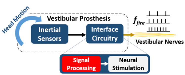
Vestibular Prosthesis (VP) block diagram. A VP mimics the operation of peripheral vestibular organs by encoding head motion into firing rate, ffire, at the vestibular nerves by means of inertial sensors and an interface circuitry. The circuitry consists of signal processing and neural stimulation blocks. Signal Processing implemented as an ASIC is reported here.
The paper is organized as follows. In Section II, we describe the signal processing functions required of a VP to replace lost peripheral vestibular function effectively. In Section III, we provide the design specifications of our signal processor followed by a detailed description of each circuit block with respect to its function. Bench test results are presented in Section IV, followed by a summary of the performance parameters and a discussion of future work in Section V. Lastly, in Section VI we highlight the significance of our study in the context of contemporary vestibular prosthesis research.
II. Vestibular Prosthesis Signal Processing
Driven by the goal of replicating the peripheral vestibular sense organs, a VP must achieve three main signal processing functions: (1) align implanted and natural inertial sensors and optimize stimulation efficacy, (2) mimic the neural dynamics of the vestibular system, and (3) generate drive signals for neural stimulators that modulate the neural firing rate of vestibular neurons.
Fig. 2 depicts a VP from the system level. At the input are analog signals G1x3(s) and A1x3(s) that represent angular velocity and linear acceleration of 3D head motion. At the output are signals (clock rates of f[GND(s)] and f[AND(s)]) to drive H-Bridge neural stimulation circuitry at rates matching firing rates of vestibular neurons [10-12]. This work pursues a signal processor that realizes functions (1)-(3) and each function is described as follows.
Fig. 2.

Vestibular prosthesis overview. The signal processor converts analog voltage outputs from inertial sensors (G1x3 and A1x3) into frequencies that match firing rates of vestibular neurons. Specifically the signal processor: (1) performs coordinate system transformation to align implanted and natural inertial sensors and optimize stimulation efficacy, (2) implements semicircular canal and otolith neural dynamics, and (3) generates clocks that can drive H-Bridge neural stimulation circuitry.
A. Coordinate System Transformation (CST)
In the peripheral vestibular system there are three SCCs and two otoliths, each with a direction of maximum sensitivity [1]. Following the surgical implantation of a VP, a coordinate system transformation, implemented as a vector-matrix multiplication, can be used to align the implanted inertial sensors with the natural SCC and otolith (Fig. 3(a)). Furthermore, the vector-matrix multiplication can also serve to improve stimulation efficacy. Small distances between adjacent SCCs/otolith organs (∼ 6 μm) can cause erroneous representation of head motion due to undesirable current spread (Fig. 3(b)). For instance, when an electrode is placed to stimulate the horizontal canal neurons, some posterior canal neurons may be falsely stimulated. Thus a coordinate system transformation can precompensate to offset anticipated current spread [13]. Functionally, the VP is required to perform matrix multiplication on analog signal triplets from the angular velocity and linear acceleration sensors (G1x3(s) and A1x3(s) in Fig. 2) to transform these signals into corrected modulation signals; GC(s)= G1x3(s)·MG,3x3(s) and AC(s)= A1x3(s)·MA,3x2(s), where MG,3x3(s) and MA,3x2(s) are 3-by-3 and 3-by-2 transformation matrices for angular and linear head motion, respectively.
Fig. 3.
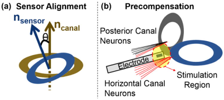
Coordinate System Transformation for the SCCs. (Redrawn from [14] (a) To align the primary axes of implanted sensors and peripheral vestibular sense organs, a vector-matrix multiplication operation can perform a coordinate system transformation between the implanted sensors and natural organs. (b) When an electrode is placed to stimulate horizontal canal neurons, a portion of posterior canal neurons can be stimulated erroneously. A vector-matrix multipler (VMM) block can precompensate for the effect and eliminate false representations of motion due to current spread.
B. Neural Dynamics
In addition to angular velocity and linear acceleration, vestibular neurons can vary their firing rates with respect to head motion frequency. Mechanically the SCCs and otoliths have a low-pass effect on neural firing rate as a function of frequency, and reduce firing rate at high frequencies. Likewise, if the frequency of head motion is very small, neural adaptation reduces the firing rates of the SCC and otolith neurons1. The dynamics are best described by the following transfer functions for the SCCs and otolith, respectively [15-17]:
| (1) |
| (2) |
In (1) and (2), typical values for the time constants are τslow=4.37 s, τfast=7 ms, τA,SCC=80 s, kA=1.2, τA,oto=11 s, and τM=46 ms. To effectively encode vestibular neural dynamic behavior, the SCC/otolith dynamics are implemented by filtering outputs from the CST block to generate GND(s) = Gc(s)·HSCC(s) and AND(s) = AC(s)·Hoto(s).
C. Firing Rate Encoding
Both the SCCs and otoliths transduce head motion into the firing rates of vestibular neurons. When the head is stationary (zero motion) the neurons fire at a constant baseline rate (∼100 Hz) [1]. If the head motion is consistent with neural excitation, the firing rate increases (∼400 Hz max.) and if the head motion is in the inhibitory direction, the firing rate decreases (∼10 Hz min.) [18]. There exists an asymmetrical (sigmoidal) dependence of firing rate with respect to head motion as indicated by the curves in Fig. 4. Based on data collected from SCC and otolith neurons four parameters define the curves; (1) baseline frequency, (2) firing rate range, (3) asymmetry ratio, and (4) gain. To optimize stimulation and comfort levels for a given patient a VP should accommodate programming of the four parameters during a rehabilitation period following implantation. The signal processor allows for varying these parameters and a firing rate encoding stage converts outputs from the neural dynamics filters into pulses having rates of f[GND(s)] and f[AND(s)].
Fig. 4.
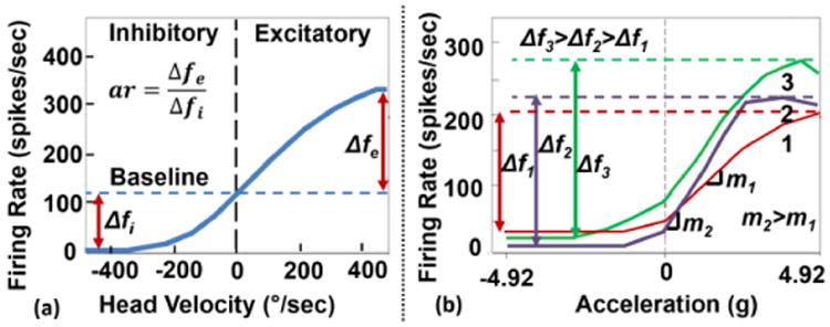
Neural firing rate vs. head motion relationships. (a) Data from an SCC neuron (redrawn from [22]). The baseline frequency is the neural firing rate when head is stationary. The asymmetry ratio, ar, is defined as the ratio of firing rates between the excitatory and inhibitory head motions. (b) Data from representative otolith neurons (redrawn from [23]). Each trace corresponds to a different otolith neuron representing a range of firing rates, Δf, and gains, m.
III. Circuit Operation
The signal processing functions discussed in the previous section can be performed purely in the analog or digital domains. A guiding design consideration was to maintain the natural human system's signal-to-noise ratio (SNR). Thus the minimum sensation levels obtained by the VP are required to match the human SCCs and otolith. In the case of the SCCs, the target SNR value can be approximated as the ratios of maximum angular velocity of normal head motion to the minimum sensation level of the SCCs. Biological data reveal that angular velocity range of head motions is ±500 °/sec [1], and the detection threshold is 2 °/sec [19]. Based on these values a mid-range SNR value of ∼48 dB is found for the SCC. For the otolith the linear acceleration range is ± 4 g, where g is the gravitational acceleration [1], the detection threshold is 15 mg [20] resulting in a similar SNR. To achieve mid-range SNR while minimizing power and area, subthreshold analog-signal-processing (ASP) techniques are more advantageous over digital [21]. In particular, processing can be achieved simpler in analog compared to digital, which reduces system complexity and therefore total area as well as the power consumption. Besides, ASP saves further power by eliminating the need for power-hungry analog-to-digital conversions. Therefore, our custom-design extensively makes use of subthreshold signal processing techniques. Each sub-block design is detailed below with the emphasis on the neural dynamics and the frequency encoding blocks.
A. Coordinate System Transformation: Vector-Matrix Multiplier
A vector-matrix multiplier (VMM) performs a 3-by-3 VMM operation for the SCCs to achieve a coordinate system transformation. The VMM design was presented previously at the 2014 Annual Int. Conf. IEEE Eng. in Medicine and Biology2 using the TSMC 0.35μm, 4-metal, 2-polysilicon process (Taiwan Semiconductor Manufacturing Ltd., Taiwan) [14]. The design in this work functionally enhances the previous work by generating the clocks for both 3-by-3 and 3-by-2 VMM operations for the SCCs and otoliths. The circuit architecture is the same in both VMMs. However, there are more circuit elements in the 3-by-3 VMM because of the greater number of output channels.
B. Neural Dynamics Filters
1) Selection of the Filter Architecture
The analog signals from the VMM block can be filtered either using only passive circuit components (R-L-C) or using both active and passive components (e.g. OPAMP-RC, OPAMP-MOSFET-C, switched-capacitor OPAMP, OTA-C filter topologies) [24-26]. Considering the lengthy time-constants of vestibular dynamics (in the order of tens of seconds), a passive filter topology is impractical—long time constants would require very large on-chip resistors and capacitors. When considering energy-efficiency and selecting active components, OTAs are advantageous over OPAMPs since they require relatively fewer MOS devices [27]. The power consumed by an OTA-C stage decreases with decreasing bandwidth. Therefore, an OTA-C filter is very desirable for the vestibular application as -3 dB bandwidths of the SCC and otolith transfer functions are very small; ∼23 Hz and ∼3.5 Hz, respectively. When an OTA is biased with a very small current value of 100 pA, to obtain a time-constant of 80 s from a 1st order stage, the capacitance value needs to be C= 154 nF. This is impractical to implement considering its large footprint. To overcome this issue, a switch that limits the effective output current of the OTA is used [28]. The switch is periodically turned on/off thereby limiting the output current, IOTA, and creating an effective current of IOTA,eff = γ·IOTA, where γ is the duty cycle of Φ, the clock that controls the switch (Fig. 5(a)). As a result very long time constants given by:
Fig. 5.
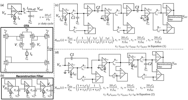
Neural dynamics filters. (a) Following [28], a switch at the output of an OTA-C stage limits the current, thereby increasing the time constant. (b) A 3rd order low-pass reconstruction filter stage is used to remove the high-frequency components of the output signals. (c) SCC neural dynamics filter schematics. (d) Otolith neural dynamics filter schematics.
| (3) |
can be achieved. In (3), UT is the thermal voltage (≈26 mV at room temperature), C is the capacitance, and Ib is the bias current of the OTA. By varying γ the pole/zero locations associated with that particular OTA-C element are controlled. This enables individual control over all pole/zero locations of the neural dynamics filters necessary to allow for patient-dependent parameters. In the design there are two additional OTA stages employed in negative feedback: one of them serving as a buffer between two stages and the other as a path for IOTA when the switch is off. The switches S1 and S2 are implemented as nMOS and pMOS devices, respectively, thereby eliminating the need for additional digital circuitry to synchronize the clock Φ and its inverse, namely Φ̄.
Higher-order neural dynamics transfer functions in (1) and (2) are implemented by cascading 1st order OTA-C filters. Filter clocks are generated using glitch circuitry [29] which generates a pulse at the rising-edge of the input clock. The glitch circuitry power consumption increases as the pulse-width of the clock increases. Therefore the duty-cycles of the filter clocks are kept small. The high-frequency components of the signals associated with clocked operation, are removed at a three-cascaded 1st order low-pass filter (Fig. 5(b)).
2) SCC Filter
The SCC neural dynamics transfer function given in (1) is decomposed into three 1st order filters; one low-pass (LPF) and two high-pass filters (HPF1 and HPF2). The first stage is the LPF, thereby enabling LPF flicker noise to be filtered by the following HPF stages. It should be mentioned that (1) is derived from firing rate data obtained from animal vestibular neurons. However, the signals filtered here are not firing rate but rather rate sensor signals, where the magnitude of the respective sensor output is proportional to the angular velocity or linear acceleration. Therefore, the gain term in (1), namely AV,SCC, is ignored when implementing the filters. The firing rate gain is controlled at the block following the filters, namely the frequency encoding block.
The schematic of the SCC filter is shown in Fig. 5(c). Capacitance values are selected such that varying the pulse-width of the associated clock, a range of time-constants, including the typical values from the biological experiments, can be obtained for a reasonably low bias current value of 100 pA. Capacitance and OTA bias current values are C1=10 pF, C2=250 pF, C3=1 nF, Ib1=1 nA, Ib2=Ib3=100 pA.
3) Otolith Filter
The transfer function is decomposed into two stages; a pole-zero doublet, and a LPF stage. The filter schematic is shown in Figure 5(d). Capacitance and OTA bias current values are C1=800 pF, C2=20 pF, Ib1=Ib2=100 pA, and Ib3=1 nA.
C. Firing Rate Encoding: Frequency Encoding Block (FEB)
1) System-Level Design
A frequency encoding block (FEB) realizes the sigmoid relationship between the head motion (either angular or linear) and the firing rate of the vestibular neurons in Fig. 3. The FEB implements three specific functions; signal conditioning, core signal processing, and clock generation (Fig. 6).
Fig. 6.

The frequency encoding block (FEB) consists of signal conditioning, core signal processing, and clock generation blocks.
The signal conditioning function involves amplification of the input signal of the FEB, which is the neural dynamics filter output signal. A variable-gain amplifier stage is designed to meet the input voltage range requirement of the signal processing sub-blocks.
The signal processing function can be grouped into two categories: introducing the asymmetric sigmoid relationship and implementing frequency modulation. A sigmoid function is implemented in an energy-efficient way by utilizing an OTA in subthreshold region as its output current is related to the input voltage through a tanh function [29]. The bias current of the OTA sets the maximum/minimum values of the output current, which are also the asymptotic maximum/minimum values of the tanh function. The linear-region gain of the OTA, and therefore that of the tanh function, is tuned by means of a linear-range control circuit. To introduce asymmetry to the sigmoid function, the variable-gain OTA output current is weighed with different constants at non-identical current mirrors. These current signals are later summed together at the output node. An offset current entering the output node sets the DC level, which is controlled to vary the baseline firing-rate of the neurons.
The frequency modulation is achieved by a current-controlled oscillator (CCO). An integrate-and-fire circuit is designed for its linear frequency-current relationship and ability to generate the frequencies of interest (fout<∼600 Hz) with very small current values (in the order of nA) [30].
The clock generation function of the FEB involves generating the clocks to control the switches of an H-Bridge circuit that generates biphasic current pulses to stimulate neurons. A pair of out-of-phase clocks is generated to control an H-Bridge. These clocks are generated by cascading three glitch circuits, which generates a pulse at the falling-edge of the input clock.
2) Variable-Gain Amplifier
Designed as a basic differential pair with resistive loads, the VGA inherently offers high output swing, high linearity, high power supply noise rejection, and simple biasing (Fig. 7(a)) [31]. The gain of the VGA is found as:
Fig. 7.
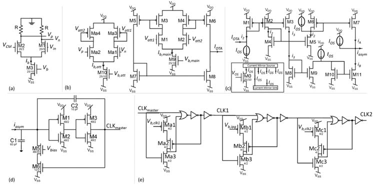
Frequency encoding blocks. (a) Variable gain amplifier. (b) Variable-gain OTA. (c) Asymmetric current mirror. The inset shows the circuit generating the offset current, IOS. (d) Current-controlled oscillator. (e) Clock generation. Three glitch circuitry are cascaded to generate two clocks (CLK1 and CLK2) that are out of phase by an interphase gap amount.
| (4) |
where R is the gain resistance, κ the gate coupling coefficient relating gate to channel surface potential, and Ib, the bias current. To lower the output common-mode voltage to a value within the input common-mode range of the next stage, namely the variable-gain OTA; the positive rail of the circuit is grounded. The VCM in Fig. 7(a) serves as the common-mode voltage for the single-ended neural dynamics filter output signals. The bias current, Ib, sets the gain and is controlled by the gate voltage, Vb, of a long-channel nMOS, M3. Gain resistor and the bias currents are R=1 MΩ and Ib= 630 nA. The maximum gain of the circuit is simulated as ∼6.5. This value is sufficiently large enough to amplify the neural dynamics filter output signals (Vmax=100 mVpp) enabling them to meet the input voltage requirement of the variable-gain OTA (Vmax=600 mVpp).
3) Variable-Gain OTA
A wide-range variable-gain OTA in subthreshold region achieves an output current-differential input voltage relationship described by a tanh function as (Fig. 7(b)) [32]:
| (5) |
where Ib,main is the bias current controlled by the bias voltage, Vb,main and α is an attenuation factor given by:
| (6) |
which is obtained through the attenuation circuit formed by Ma1-Ma4 and set by the bias current, Ib,att, controlled by the gate voltage of M10, namely Vb,att. In (6), K is the transconductance parameter, which is a function of mobility and unit gate-oxide capacitance, and (W/L)Ma1 is the aspect ratio of transistors Ma1-Ma2. It should be emphasized that (6) is valid only when Ma1-Ma2 and Ma3-M4 are in deep inversion and subthreshold regions, respectively [32]. This condition limits the allowed values for Ib,att, which creates a lower and an upper bound for α. The boundary values of α are particularly important in determining the variable-gain OTA input voltage range, which corresponds to normal head motion angular velocity/linear acceleration ranges mapped into neural firing-rates. To allow a wide-range of attenuation factor, the ratio of the sizes of Ma1 (Ma2) to Ma3 (Ma4) is kept very small, (W⁄L)Ma1=1/100 and (W⁄L)Ma3=200/1. Large M1 and M2 devices ((W⁄L)M1,M2=20/3) ensure subthreshold operation for a wide range of bias currents (Ib,att<∼3 μA, Ib,main<∼3 μA). M9 and M10 are sized as long devices ((W⁄L)M9,M10=25/10) to reduce the effect of channel-length-modulation. To enable improved matching, all current mirrors are cascoded structures.
In the design process, a series of curves obtained by simulations were compared to a modified version of the mathematical expression corresponding to the biological data in [33]. The modifications to the original expression in [33] involve removal of the parameters that model the asymmetry, normalize of the magnitude to 1, and change its input variable from 12-bit digitized angular velocity to angular velocity, ω. Based on simulations, for an input voltage range of ±300 mV, the desired steepness that matches with the biological sigmoid curve can be obtained.
4) Asymmetric Current Mirror
An asymmetric current mirror stage consisting of a series of current mirrors is designed to reflect the asymmetry in the firing rate vs. head motion relationship corresponding to the range of excitatory and inhibitory head motions (Fig. 3). Essentially, the circuit combines two separate lines to generate a piecewise linear function (Fig. 7(c)) [34]. The output current of the variable-gain OTA, IOTA, is subtracted from an offset current, namely IOS, which is generated as the drain-to-source current of a long-channel nMOS (W/L=25 μm/10μm) and controlled by an offset voltage, namely VOS, applied to the gate of the nMOS (Fig. 7(c) inset). IOS is replicated using current mirrors (source and sink). The resultant current, i1, is replicated twice to generate i2 and i3, where i1=i2=i3=IOS-IOTA. Each replica is fed to one of the two current mirror pairs formed by M4-M7 and M8-M11 to generate iA and iB. Because M6-M7 pair is a sink-input current mirror, iA is non-zero only when IOTA<0. Likewise, M10-M11 is a source-input current mirror, thereby creating a non-zero iB only if IOTA>0. The output of the asymmetric current mirror; iasym, which is obtained by summation of IOS, iA, and −iB at the output node; is asymmetric across the horizontal IOS level. The exact expression of iasym is as follows:
| (7) |
where m = (W/L)M7⁄(W/L)M6 and n = (W/L)M11⁄(W/L)M10 and m≠n. All current mirrors are designed as cascode structures to reduce mirroring errors. The current mirrors formed by M1-M3, M4-M5, and M8-M9 have unity current-gains. Typical asymmetry ratio values, ar, in Fig. 3 vary between 2 and 4. To vary the ar, which is given by ar=m/n, within that range, m is set to m=4 and four M11s having n values between 1 and 2 have been implemented. The ar values are varied by changing the M11 connected to the circuit by means of a 1-to-4 line demultiplexer consisting of minimum-size transmission-gates.
5) Current-Controlled Oscillator (CCO)
The current output from the asymmetric current mirror stage is fed to a CCO to generate a master clock, namely CLKmaster. The CCO is a modified version of a self-resetting neuron circuit [29] (Fig. 7(d)). Setting the capacitor C2=10 pF, the output frequency range meets the normal firing-rate range observed at the vestibular neurons (ffire<600 Hz) for a small input current range (iin<20 nA). When the low-to-high and high-to-low transitions occur, jumps at the output voltage are reflected to the input through the capacitive divider formed by C1 and C2. The C1 capacitor is set to 60 pF, thereby ensuring the voltage jumps at the input node are sufficiently large to go above and below the switching thresholds of the M1-M2 inverter.
6) Glitch Circuitry
Two clocks (CLK1, CLK2) are generated from the CLKmaster. CLK1 and CLK2 are out of phase by the interphase gap (IPG). A triple cascaded glitch circuitry is designed to generate both clocks (Fig. 7(e)). With this configuration, pulse-widths of CLK1, CLK2, and the IPG can be controlled by their respective bias voltages, Vb,clk1, Vb,ipg, and Vb,clk2.
IV. Experimental Results
The design was fabricated in TI 0.35 μm two-polysilicon, three-metal CMOS process (Texas Instruments, Inc., Dallas, TX). Optical images and floor plans corresponding to each block are shown in Fig. 8. The footprints of the 3-by-3 VMM, the SCC filter, the otolith filter, and the V-to-F stage are 1 × 0.73 mm2, 1.42 × 1.14 mm2, 1.34 × 1 mm2, and 0.47 × 0.65 mm2, respectively. In the following sub-sections, a description of the testing procedure, functional verification, noise, and power performance of each block, as well as system-level measurements are presented. Lastly, a performance summary and comparison with state-of-the-art VP signal processing systems are presented.
Fig. 8.
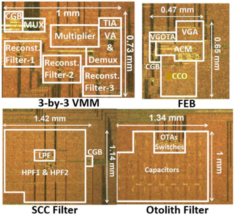
Optical die images and floor plans. The abbreviations FEB, CGB, VA, ACM, CCO, and VGOTA refer to the frequency encoding block, clock generation block, voltage averaging, asymmetric current mirror, current controlled oscillator, and the variable-gain OTA blocks.
A. Testing Procedure
Each block was tested individually followed by system-level tests. All bias currents were generated externally by off-chip reference circuitry. All time and frequency domain analyses of signals were performed using a Tektronix DPO 3014 oscilloscope (Textronix, Beaverton, OR) and an HP 35665A signal analyzer (Hewlett-Packard Co., Palo Alto, CA), respectively. Particular instruments and software used in measurements of each block are mentioned within the associated sub-section.
B. Individual Block Evaluation
1) Vector-Matrix Multiplier (VMM)
The VMM weight voltages were generated by dual channel Keithley 2636A (Keithley Instruments Solon, OH) sourcemeters. Input clock of the VMM was generated using an TI MSP430 series microcontroller. To verify the linearity of the VMM, a sinusoidal signal that represents a gyroscope output was connected to all three sensor inputs. Additionally, a weight voltage varying from -200 mV and 200 mV was connected to all nine weight inputs. For two different input signal magnitudes, the output varies linearly with the weight voltages as shown in Fig. 9(a). The outputs shown in Fig. 9(b) verify the VMM operation when a 3.5 Hz sinusoidal signal is multiplied by the weight elements, .
Fig. 9.
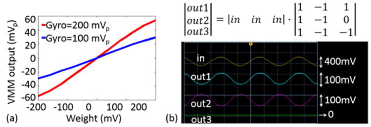
VMM measurements obtained from the 3-by-3 VMM. (a) Linear dependence of the VMM output (y-axis) with respect to the input signal magnitudes (x-axis). The results were parametrized by gyroscope output voltages (200 mVpp and 100 mVpp.). (b) The 3-by-3 matrix multiplication was verified when a 400 mVpp sinusoidal signal at 3.5 Hz was multiplied by the 3-by-3 matrix shown above the measured waveforms.
The non-ideal sampling at the sensor and weight voltage multiplexing stage has a low-pass effect with a -3dB frequency >1 kHz. On the other hand, the reconstruction filter bandwidth is smaller (≈500 Hz), thereby setting the VMM bandwidth to f-3dB,VMM=∼500 Hz. The noise measurement was performed over the bandwidth of normal head motions (f<∼20 Hz) revealing a measured VMM input-referred noise power of .
2) Neural Dynamics Filters
Functionalities of both SCC and otolith filters were verified by extracting gain plots of each 1st order stage. To explore the pole/zero ranges of each stage, externally generated clocks were used. The frequency response of each stage was measured using a 100 mVpp sinusoidal signal as the input. By varying the clock pulse width of the stage (PW), the shift in pole/zero locations were verified (Fig. 10). Then, frequency responses that match with typical values of the neural dynamics were obtained for both filters (Fig. 11). The SCC filter overall frequency response was obtained using clocks generated by the on-chip clock generation block. The output noise power of the SCC filter, which uses on-chip generated clocks, was measured as vn,in-SCCfilter2=47 nV2 for f<20 Hz. Supplied by ±1.6 V, the power consumptions of the SCC and the otolith filters were measured as 6.96 μW and 1.2 μW, respectively. The higher power consumption of the SCC filter is attributed to the power consumption of the on-chip generation block.
Fig. 10.
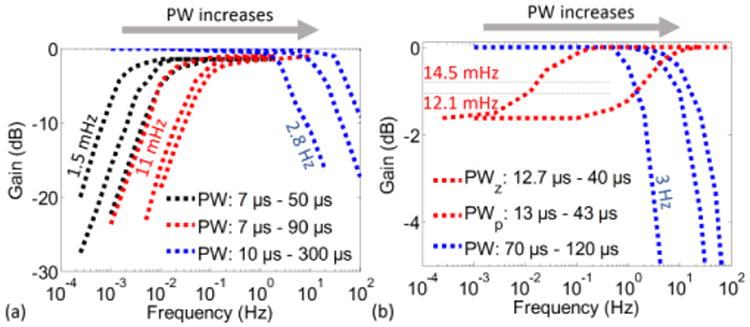
Control of pole/zero locations for (a) SCC neural dynamics filter stages and (b) Otolith neural dynamics filter stages. PW corresponds to the pulse width of the clock controlling the switch at each 1st order filter stage.
Fig. 11.
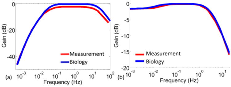
Complete transfer function measurements compared to neural dynamics plotted using typical values from physiological measurements. (a) SCC filter. (b) Otolith filter.
3) Frequency Encoding Block (FEB)
The input to the FEB was generated by a function generator. For frequency measurements, NI LabVIEW SignalExpress software (National Instruments, Austin, TX) was used to acquire oscilloscope data. The maximum gain of the VGA stage was measured as AVGA=6.48 V/V which is close to the design target value of 6.5. The frequency measurements were made for 11 data points spanning the variable-gain OTA input voltage range of ±300 mV. For each data point ∼10 frequency measurements were performed, which were averaged using MATLAB (Mathworks Inc., Natick, MA).
Measurement results are shown in Fig. 12. For a fixed Vb,main=-1.1 V, and when varying Vb,att from -1.14 V to -1.2 V, the slope control (and therefore the linear range control) of the frequency-input voltage was verified (Fig. 12(a)). The linear ranges of the curves span the values between 176 °/sec and 500 °/sec. As desired the excitatory linear range of VL,bio,exc=246.5 °/sec is included. For a fixed Vb,att, by varying Vb,main, the range of the output frequency was controlled as shown in Fig. 12(b). Fig. 12(c) illustrates the control over the order of symmetry. By varying the select bits the asymmetry ratio can take on four distinct values between 2 and 4. The baseline frequency was controlled by varying the offset voltage bias, namely VOS, of the asymmetric current mirror. A 5 mV change in the VOS results in 56 Hz of difference in the baseline frequency (Fig. 12(d)).
Fig. 12.
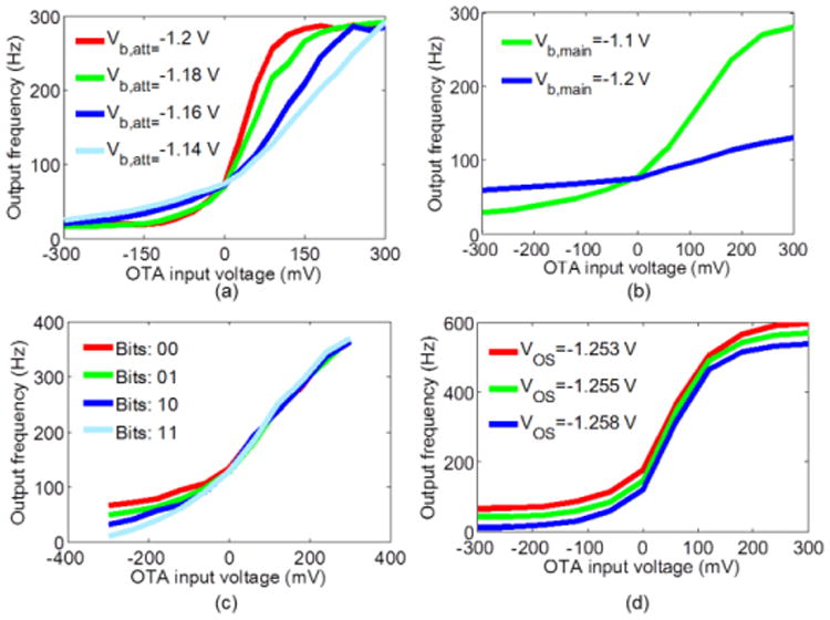
Measurement results of the current to frequency conversion block. (a) Slope control. (b) Frequency range control. (c) Order of asymmetry control. (d) Baseline frequency control.
Fig. 13 illustrates the measurement results corresponding to the output clocks, CLK1 and CLK2. The minimum pulse duration (PD) and IPG can be adjusted to less than 1 μs. Upper boundary for the PD and IPG is limited by the corresponding pulse rate. As a demonstration when PD=IPG, PD varied from 5 μs to 630 μs when Vb,clk1, Vb,ipg, and Vb,clk2 varied from ∼1.184 V to ∼1.354 V.
Fig. 13.

Measured CLK1 and CLK2 waveforms. The pulse duration (PD) and the interphase gap (IPG) can be varied from <1 μs to the maximum possible value for that particular frequency (630 μs when PD=IPG and clock frequency is 400 Hz). For PD=5 μs, 100 μs, and 630 μs, Vb,clk values are ∼1.184 V, ∼1.287 V, and ∼1.354 V, respectively.
Noise of the FEB at a certain frequency is observed as jitter in the time- domain. The noise power at that frequency can be found by measuring the variance of the frequency distribution [35]. Vestibular sensation threshold refers to the minimum angular/linear motion that causes a perception of the motion when in a steady position. Therefore, noise measurements were performed by measuring the variance of a frequency distribution obtained out of 512 frequency measurements centered around a baseline frequency of ∼70 Hz3. The measured output frequency noise power was reflected to the input to give . For a typical vestibular neuron firing rate maximum value of 300 Hz, the maximum power consumption was measured as 405 μW.
C. System-Level Measurements
For system-level measurements, the signal processor was biased with off-chip reference circuitry. The system-level tests included dynamic range, noise, and response time measurements. For dynamic range measurements, a sinusoidal signal, Vs, within the pass-band (f=0.5 Hz) of the processor was supplied to the two randomly selected sensor inputs of the system. The pulse waveform at the selected channel output was captured using the oscilloscope for a total of 22 Vs magnitude values within the VMM input dynamic range (20 mVpp to 400 mVpp) when the weight voltages were set to 400 mVpp ([1 1 1]). For each Vs magnitude value, the measurement lasted for 40 seconds (20 cycles). The waveforms were then processed using MATLAB to find the average maximum and minimum frequency values corresponding to each weight voltage. Two plots illustrating the output pulse rate variation with input signal magnitude for both SCC and otolith channels are presented in Fig. 14(a). For input dynamic range measurements, the Vb,att of the FEB was set to Vb,att= ∼-1.14 V, which creates a linear dependence between the output frequency and the FEB input. The input signal range that ensures linear operation with a maximum degradation of 5% for both channels was measured as ±200 mV. The output dynamic ranges for both channels were measured as >1 kHz. Noise measurements of the system were performed following the same approach explained in the FEB noise analysis. The output frequency noise power obtained around a baseline frequency of ∼100 Hz was referred to the input of the signal processor for both SCC and otolith channels. Minimum detectable head motion values were calculated from the measured input-referred noise values for gyroscopes and accelerometers having sensitivities of 0.4 mV/°/sec and 50 mV/g. To obtain upper boundaries for the processor response times, input and output waveforms were monitored when the input was reduced from 0 V to -200 mV, which correspond to no head motion (baseline pulse rate of ∼100 Hz) and maximum angular / linear inhibitory head motion (minimum pulse rate of ∼30 Hz), respectively. To prevent low-frequency attenuation at the filter stages, rather than a step signal, a 0.5 Hz sawtooth signal was used as the input (Fig. 14(b)). The time delay between the sharp drop of the input signal and the first pulse generated following the drop was measured for ∼20 cycles, which were then averaged to extract the upper boundaries for the processor response times.
Fig. 14.
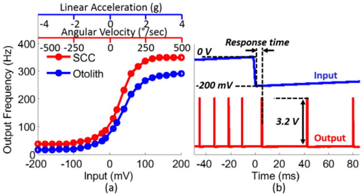
System-level measurements. (a) Output pulse rate dependence on input for SCC and otolith channels. The channels were supplied with non-identical bias values. (b) Response time measurements. The response time of the processor is expected to increase with decreasing output pulse rate. Therefore, to obtain upper boundary values, the processor was supplied by a 0.5 Hz sawtooth signal varying between 0 V and -200 mV, which correspond to no head motion and maximum angular / linear inhibitory head motion, respectively. Time delay between sawtooth drop onset and the first pulse following the onset were measured for ∼20 cycles, which were then averaged to obtain the response times for both SCC and otolith channels. For clarity, input and output waveforms corresponding to only the SCC channel are presented.
D. Performance Summary and Comparison
The ASIC realizes signal processing functions needed for a VP and enables control over all patient-dependent parameters. Tables I and II summarize all the performance parameters. It is noteworthy to highlight that to achieve low power operation, the VMM and the neural dynamics filters are limited to a few μWs of consumed power. In addition, the ASIC can be interfaced with analog output gyroscopes or accelerometers having sensitivities as large as 0.4 mV/°/sec and 50 mV/g respectively. The upper bound for the response time of the ASIC was measured as 12 ms, which is longer than the minimum human vestibuloocular reflex latency of 7 ms [39]. There are two blocks contributing the response time: the VMM that operates in a time-division-multiplexed manner and the FEB, which has a response time having output pulse rate dependence.
Table I. Summary of Performance Parameters.
| Property | 3-by-3 VMM | SCC Filter | Otolith Filter | Frequency Encoding |
|---|---|---|---|---|
| Power | 5.1 μW | 6.96 μW | 1.2 μW | 405 μW |
| Area | 0.73 mm2 | 1.62 mm2 | 1.34 mm2 | 0.31 mm2 |
| SNR | 48.73 dB | 42 dB | N/A | 35 dB |
| Input/output voltage range | ±200 mV / ±50 mV | ±50 mV / ±39 mV | ±50 mV / ±50 mV | >±46.3 mV / N/A |
| Time Constant Range | N/A | 3.92 ms -106 s | 3.6 ms – 13.2 s | N/A |
| Maximum Output Frequency | N/A | N/A | N/A | > 1 kHz |
| Asymmetry Ratio Range (Δfexc/Δfinh) | N/A | N/A | N/A | 2 – 4 |
| CLK1-CLK2 PD & IPG | N/A | N/A | N/A | > ∼1 μs |
Table II. Summary of System-Level Measurements.
| Property | SCC | Otolith |
|---|---|---|
| Input dynamic range | ±200 mV | ±200 mV |
| Output dynamic range | > 1 kHz | > 1 kHz |
| Input-referred noise | 3.5 mVrms | 2.8 mVrms |
| Minimum detectable head motion | 12.4 °/sec | 78 mg |
| Response time | < 12 ms | < 12 ms |
Table III outlines a comparison of the ASIC with state-of-the-art VP systems. For clarity CST, ND, and FE refer to coordinate system transformation, neural dynamics, and frequency encoding, respectively. While it is challenging to compare the host of approaches to realizing a VP, it is useful to examine the contributions of each. For example, when compared with systems using off-the-shelf components and processors [4, 6, 36], the signal processor ASIC has the advantage of energy-efficiency and small footprint without compromising the functionality. Our design advances the other custom design reported in [5, 37, 38] through a coordinate system transformation, which could potentially improve stimulation efficacy [13].
Table III. State-of-the-art VP Signal Processors.
| This work1 | Johns Hopkins [4, 36] | Imperial / UCY2 [5, 37, 38] | CLONS3 [6] | ETH Zürich / Scuola Superiore [7] | |
|---|---|---|---|---|---|
| Technology | ASIC (TI 0.35μm CMOS) | Commercial μcontroller | ASIC (AMS 0.35μm CMOS) | Commercial Signal Processing Platform | Hybrid analog and digital off-the-shelf and ASIC components |
| Functionsa | CST (3 SCCs or 2 otoliths) ND+FM (2 SCCs and 1 otolith) | CST+ND+FM+AM (3 SCCs) | ND+AM (3 SCCs and 2 otoliths) | CST+ND+FM+AM (3 SCCs) | ND+FM (3 SCCs and 2 otoliths) |
| Area | 6.22 mm2 | 81 mm2 | 1.19 mm2 | 8202 mm2 | Not reported |
| Power | 1.24 mW | 12 mW | 53.8 μW (1 SCC and 1 otolith) | Not reported | Not reported |
Bias voltages and currents are generated externally. The processor does not include digital circuit blocks necessary for programming (e.g., memory elements, D/A converters).
Measurement results for the SCC processor are not reported.
The system is not designed as a prosthetic device but as a research development platform. The area of the system is presented for the sake of completeness.
CST: Coordinate System Transformation, ND: Neural Dynamics, FM: Frequency Modulation, AM: Amplitude Modulation
To compare the power efficiencies of analog and digital signal processing for a VP realized with a microcontroller, the functions designed here were also implemented on a low-power TI MSP430 series microcontroller. The MSP430 chip occupies an area of 302.7 mm2 and draws 7 mA of current from a 3.2 V of supply voltage, implying 22.4 mW of power consumption. From noise measurements, the minimum detectable angular velocity and linear acceleration values for the MSP430 were found as 2.3 °/sec and 18.5 mg, respectively. Based on the power and dimension values summarized in Table I, it is estimated that an ASIC performing the signal processing functions in a VP for all three SCCs and two otoliths would consume 2.1 mW, occupying 10.5 mm2 of chip area. The measured power values of the ASIC do not include power values from the memory and the DAC circuitry that are needed to assist the core signal processing circuitry. However, with careful design of those blocks, current consumption of the custom ASIC could still be kept one order of magnitude less than the microcontroller power. Based on noise measurements of the ASIC summarized in Table II and the MSP430, minimum detectable angular velocity and linear acceleration values of both solutions exceed the requirements of the biology. However, the noise performance of the ASIC can be improved to potentially match the sensing thresholds of the vestibular organs.
V. Discussion and Future Work
The measurement results verify the low-power operation of the VMM and the neural dynamics filters of the ASIC. Considering ways to improve upon the system, we first consider power. The FEB power is most dramatically affected by the CCO especially the inverters formed by M1-M4 in Fig. 7(d). During the times when the input node of the CCO stays at a potential between the two rail voltages, inverters dissipate significant static power. A method to limit the static power consumption would be to reduce the sizes of M1-M4. Simulation results show that reducing (W⁄L)M1-M4 from 48/2 to 0.9/20, the CCO power consumption decreases drastically.
The second improvement that can be made is with the noise performance, which in turn would improve the detection thresholds for head motion. Using noise measurements from the overall system, the detection thresholds for angular and linear motions were calculated as 12.4 °/sec and 78 mg, respectively. As an effort to meet the detection thresholds of the SCCs (2 °/sec) and otoliths (15 mg) three modifications can be done on the circuit: (1) Changing the transconductance elements from nMOS-input to pMOS-input to reduce the flicker noise, (2) Increasing input transistor dimensions of the transconductance elements to reduce both the flicker and the kT/C noise, and (3) Preparing a PCB for the ASIC to reduce the susceptibility of the wires to EM noise pickup.
The third improvement that can be made is designing additional circuitry that would enable amplitude modulation as an encoding method alternative to or in conjunction with the frequency modulation. Human and animal studies have shown that both frequency and amplitude modulation could serve as effective modulation strategies [40-42]. To achieve this flexibility a current controlled current source can generate a stimulation current that is linearly dependent upon the output of the asymmetric current mirror. Selection of modulation strategy (i.e., frequency modulation, amplitude modulation, a combination of both) can be achieved by a multiplexer block.
Finally, the ASIC can be integrated with additional blocks to build a complete VP. These blocks would include: (1) Digital blocks to program the design (e.g. memory elements, D/A converters, a digital communication block), (2) Power management blocks (e.g. wireless link to transmit power to the implant units), (3) A current stimulation block to stimulate the neurons, and (4) Inertial sensors.
VI. Conclusion
The signal processor ASIC reported here implements three critical features of a vestibular prosthesis. First, with functionality that can be determined by patient-dependent parameters (e.g. matrix weights, stimulation frequency range, etc.), stimulation efficacy may be improved. Second, the ASIC is energy efficient and, third, the ASIC presents a small footprint. When combined with focused stimulation and low-power inertial sensors [43] the ASIC lays a promising foundation for building a battery-operated small footprint prosthetic device to overcome vestibular loss for patients suffering from bilateral vestibular dysfunction.
Acknowledgments
The authors thank Texas Instruments for their generous support and Dr. Kemal Demirci for his help in fabricating the devices. The authors also thank three anonymous reviewers for helpful comments that served to strengthen the impact of this work.
This work was supported in part by the National Science Foundation under Grant ECCS-0927103, CAREER ECCS-1055801, and by the National Center for Advancing Translational Sciences of the National Institutes of Health under Award Number UL1TR000454, KL2TR000455.
Biographies

Hakan Töreyin (S′11, M′14) received the B.S. degree in electrical and electronics engineering from Middle East Technical University, Ankara, Turkey, and the M.S. and the Ph.D. degrees in electrical and computer engineering from Georgia Institute of Technology, Atlanta in 2007, 2008, and 2014, respectively. Dr. Töreyin is currently a postdoctoral researcher in the School of Electrical and Computer Engineering at Georgia Institute of Technology. In 2007-2008 he was a Fulbright Fellow and in 2012 he was awarded the Chih Foundation Research Award. At the IEEE EMBC 2014 Student Paper Competition, he was recognized as the North America Finalist and awarded the third prize. Dr. Töreyin's research interests include energy-efficient circuits and systems design for wearable and prosthetic biomedical applications.

Pamela Bhatti (M′05) received the B.S. degree in bioengineering from the University of California, Berkeley, the M.S. degree in electrical engineering from the University of Washington, Seattle, and the Ph.D. degree in electrical engineering, with an emphasis on micro-electro mechanical systems (MEMS), from the University of Michigan, Ann Arbor, in 1989, 1993, and 2006, respectively. She is an Associate Professor in the School of Electrical and Computer Engineering, Georgia Institute of Technology, Atlanta. Before completing her Ph.D. degree, she researched the detection of breast cancer with ultrasound imaging at the University of Michigan's Department of Radiology (1997–1999). Her industry experience includes embedded systems software development at Microware Corporation, Des Moines, IA (1996–1997), local operating network applications development and customer support at Motorola Semiconductor, Austin, TX (1994–1995), and research and fabrication of controlled-release drug delivery systems at Alza Corporation, Palo Alto, CA (1986–1990). Dr. Bhatti received the NSF Career Award in 2011. Committed to translating technology to the clinical setting, from 2011-2013 she was KL2 Scholar with the Atlanta Clinical and Translations Sciences Institute (ACTSI) and currently serves as the ACTSI's Research, Education, Training and Career Development Director for Georgia Tech. Dr. Bhatti is also an Associate Scientific Advisor for Science Translational Medicine where she contributes monthly Editor's Choice articles.
Footnotes
Adaptation is defined as the reduction in neuron firing rates during prolonged stimulation [1].
This paper was recognized as the North America Geographic Finalist in the Student Paper Competition and 3rd place in the Oral Presentation Competition.
For system-level noise measurements, the baseline frequency observed in humans (100 Hz) was used.
References
- 1.Goldberg JM, Wilson VJ, Cullen KE, Angelaki DE, Broussard DM, Buttner-Ennever J, et al. The Vestibular System: a SixthSense. 2012 [Google Scholar]
- 2.Horak F, Jones-Rycewicz C, Black FO, Shumway-Cook A. Effects of vestibular rehabilitation on dizziness and imbalance. Otolaryngology--head and neck surgery: official journal of American Academy of Otolaryngology-Head and Neck Surgery. 1992;106:175–180. [PubMed] [Google Scholar]
- 3.Gong W, Merfeld DM. Prototype neural semicircular canal prosthesis using patterned electrical stimulation. Annals of biomedical engineering. 2000;28:572–581. doi: 10.1114/1.293. [DOI] [PubMed] [Google Scholar]
- 4.Chiang B, Fridman GY, Dai C, Rahman M, Della Santina CC. Design and performance of a multichannel vestibular prosthesis that restores semicircular canal sensation in rhesus monkey. Neural Systems and Rehabilitation Engineering, IEEE Transactions on. 2011;19:588–598. doi: 10.1109/TNSRE.2011.2164937. [DOI] [PMC free article] [PubMed] [Google Scholar]
- 5.Constandinou TG, Georgiou J, Toumazou C. A neural implant asic for the restoration of balance in individuals with vestibular dysfunction. Circuits and Systems, 2009 ISCAS 2009 IEEE International Symposium on. 2009:641–644. [Google Scholar]
- 6.Nguyen T, Ranieri M, DiGiovanna J, Peter O, Genovese V, Perez Fornos A, et al. A Real-Time Research Platform to Study Vestibular Implants With Gyroscopic Inputs in Vestibular Deficient Subjects. Biomedical Circuits and Systems, IEEE Transactions on. 2014;8:474–484. doi: 10.1109/TBCAS.2013.2290089. [DOI] [PubMed] [Google Scholar]
- 7.Corradi F, Zambrano D, Raglianti M, Passetti G, Laschi C, Indiveri G. Towards a Neuromorphic Vestibular System. Biomedical Circuits and Systems, IEEE Transactions on. 2014;8:669–680. doi: 10.1109/TBCAS.2014.2358493. [DOI] [PubMed] [Google Scholar]
- 8.Jiang D, Cirmirakis D, Demosthenous A. A vestibular prosthesis with highly-isolated parallel multichannel stimulation. Biomedical Circuits and Systems, IEEE Transactions on. 2015;9:124–137. doi: 10.1109/TBCAS.2014.2323310. [DOI] [PubMed] [Google Scholar]
- 9.Andreou CM, Pahitas Y, Georgiou J. Bio-Inspired Micro-Fluidic Angular-Rate Sensor for Vestibular Prostheses. Sensors. 2014;14:13173–13185. doi: 10.3390/s140713173. [DOI] [PMC free article] [PubMed] [Google Scholar]
- 10.Jiang D, Demosthenous A, Perkins T, Liu X, Donaldson N. A stimulator asic featuring versatile management for vestibular prostheses. Biomedical Circuits and Systems, IEEE Transactions on. 2011;5:147–159. doi: 10.1109/TBCAS.2011.2138139. [DOI] [PubMed] [Google Scholar]
- 11.Constandinou TG, Georgiou J, Toumazou C. A partial-current-steering biphasic stimulation driver for vestibular prostheses. Biomedical Circuits and Systems, IEEE Transactions on. 2008;2:106–113. doi: 10.1109/TBCAS.2008.927238. [DOI] [PubMed] [Google Scholar]
- 12.Bhatti PT, Töreyin H, Hasler PE. A neural stimulator for a vestibular prosthesis utilizing a low-power field-programmable analog array; in Proc of the 8th IASTED International Conference on Biomedical Engineering, ACTA Press; 2011. pp. 723–097. [Google Scholar]
- 13.Fridman GY, Davidovics NS, Dai C, Migliaccio AA, Della Santina CC. Vestibulo-ocular reflex responses to a multichannel vestibular prosthesis incorporating a 3d coordinate transformation for correction of misalignment. Journal of the Association for Research in Otolaryngology. 2010;11:367–381. doi: 10.1007/s10162-010-0208-5. [DOI] [PMC free article] [PubMed] [Google Scholar]
- 14.Töreyin H, Bhatti PT. A low-power, time-division-multiplexed vector matrix-multiplier for a vestibular prosthesis; Engineering in Medicine and Biology Society (EMBC), 2014 36th Annual International Conference of the IEEE; 2014. pp. 6000–6003. [DOI] [PMC free article] [PubMed] [Google Scholar]
- 15.Fernandez C, Goldberg JM. Physiology of peripheral neurons innervating semicircular canals of the squirrel monkey. ii. Response to sinusoidal stimulation and dynamics of peripheral vestibular system. J Neurophysiol. 1971;34:661–675. doi: 10.1152/jn.1971.34.4.661. [DOI] [PubMed] [Google Scholar]
- 16.Fernandez C, Goldberg JM. Physiology of peripheral neurons innervating otolith organs of the squirrel monkey. III. Response dynamics. Journal of neurophysiology. 1976;39:996–1008. doi: 10.1152/jn.1976.39.5.996. [DOI] [PubMed] [Google Scholar]
- 17.Jones GM, Milsum J. Frequency—response analysis of central vestibular unit activity resulting from rotational stimulation of the semicircular canals. The Journal of physiology. 1971;219:191–215. doi: 10.1113/jphysiol.1971.sp009657. [DOI] [PMC free article] [PubMed] [Google Scholar]
- 18.Baloh R, Honrubia V. Clinical neurophysiology of the vestibular system. 3rd. Oxford Univ Press; 2001. [PubMed] [Google Scholar]
- 19.Squires TM. Optimizing the vertebrate vestibular semicircular canal: could we balance any better? Physical review letters. 2004;93:198106. doi: 10.1103/PhysRevLett.93.198106. [DOI] [PubMed] [Google Scholar]
- 20.Yu XJ, Dickman JD, Angelaki DE. Detection thresholds of macaque otolith afferents. The Journal of Neuroscience. 2012;32:8306–8316. doi: 10.1523/JNEUROSCI.1067-12.2012. [DOI] [PMC free article] [PubMed] [Google Scholar]
- 21.Sarpeshkar R. Efficient precise computation with noisy components: extrapolating from an electronic cochlea to the brain. California Institute of Technology. 1997 [Google Scholar]
- 22.Sadeghi SG, Minor LB, Cullen KE. Response of vestibular-nerve afferents to active and passive rotations under normal conditions and after unilateral labyrinthectomy. Journal of neurophysiology. 2007;97:1503–1514. doi: 10.1152/jn.00829.2006. [DOI] [PubMed] [Google Scholar]
- 23.Fernandez C, Goldberg JM. Physiology of peripheral neurons innervating otolith organs of the squirrel monkey. II. Directional selectivity and force-response relations. Journal of neurophysiology. 1976;39:985–995. doi: 10.1152/jn.1976.39.5.985. [DOI] [PubMed] [Google Scholar]
- 24.Harrison J, Weste N. A 500 MHz CMOS anti-alias filter using feedforward op-amps with local common-mode feedback; Solid-State Circuits Conference, 2003 Digest of Technical Papers ISSCC 2003 IEEE International; 2003. pp. 132–483. [Google Scholar]
- 25.Castello R, Gray PR. A high-performance micropower switched-capacitor filter. Solid-State Circuits, IEEE Journal of. 1985;20:1122–1132. [Google Scholar]
- 26.Zhang X, El-Masry E. A novel CMOS OTA based on body-driven MOSFETs and its applications in OTA-C filters. Circuits and Systems I: Regular Papers, IEEE Transactions on. 2007;54:1204–1212. [Google Scholar]
- 27.Sarpeshkar R. Ultra Low Power Bioelectronics: Fundamentals, Biomedical Applications, and Bio-Inspired Systems. Cambridge University Press; 2010. [Google Scholar]
- 28.Rodriguez-Villegas E, Casson AJ, Corbishley P. A subhertz nanopower low-pass filter. Circuits and Systems II: Express Briefs, IEEE Transactions on. 2011;58:351–355. [Google Scholar]
- 29.Töreyin H, Bhatti P. A field-programmable analog array development platform for vestibular prosthesis signal processing. Biomedical Circuits and Systems, IEEE Transactions on. 2013;7:319–325. doi: 10.1109/TBCAS.2012.2216525. [DOI] [PMC free article] [PubMed] [Google Scholar]
- 30.Mead C. Analog VLSI and Neural Systems. Addison-Wesley; 1989. [Google Scholar]
- 31.Razavi B. Design of Analog CMOS Integrated Circuits. McGraw-Hill; 2001. [Google Scholar]
- 32.DeWeerth SP, Patel GN, Simoni MF. Variable linear-range subthreshold OTA. Electronics Letters. 1997;33:1309–1311. [Google Scholar]
- 33.Dai C, Fridman GY, Davidovics NS, Chiang B, Ahn JH, Della Santina CC. Restoration of 3D vestibular sensation in rhesus monkeys using a multichannel vestibular prosthesis. Hearing research. 2011;281:74–83. doi: 10.1016/j.heares.2011.08.008. [DOI] [PMC free article] [PubMed] [Google Scholar]
- 34.Kettner T, Heite C, Schumacher K. Analog CMOS realization of fuzzy logic membership functions. Solid-State Circuits, IEEE Journal of. 1993;28:857–861. [Google Scholar]
- 35.Palermo S. In: “Noise” D o E a C E class notes for ECEN 474. Texas A&M University, editor. Fall. 2012. [Google Scholar]
- 36.Hageman KN, Kalayjian ZK, Tejada F, Chiang B, Rahman M, Fridman GY, et al. A CMOS Neural Interface for a Multichannel Vestibular Prosthesis. Biomedical Circuits and Systems, IEEE Transactions on. 2015 doi: 10.1109/TBCAS.2015.2409797. [DOI] [PMC free article] [PubMed] [Google Scholar]
- 37.Constandinou TG, Georgiou J, Toumazou C. A fully-integrated semicircular canal processor for an implantable vestibular prosthesis; Electronics, Circuits and Systems, 2008 ICECS 2008 15th IEEE International Conference on; 2008. pp. 81–84. [Google Scholar]
- 38.Constandinou TG, Georgiou J. A micropower tilt-processing circuit. Biomedical Circuits and Systems, IEEE Transactions on. 2009;3:363–369. doi: 10.1109/TBCAS.2009.2027421. [DOI] [PubMed] [Google Scholar]
- 39.Amin MS, Konrad H, Konrad H. Vestibuloocular reflex testing. E-Medicine Journal. 2001 Jul;20 [Google Scholar]
- 40.Van De Berg R, Guinand N, Nguyen TK, Ranieri M, Cavuscens S, Guyot JP, et al. The vestibular implant: frequency-dependency of the electrically evoked vestibulo-ocular reflex in humans. Frontiers in systems neuroscience. 2014;8 doi: 10.3389/fnsys.2014.00255. [DOI] [PMC free article] [PubMed] [Google Scholar]
- 41.Fornos AP, Guinand N, van de Berg R, Stokroos R, Micera S, Kingma H, et al. Artificial balance: restoration of the vestibulo-ocular reflex in humans with a prototype vestibular neuroprosthesis. Frontiers in neurology. 2014;5 doi: 10.3389/fneur.2014.00066. [DOI] [PMC free article] [PubMed] [Google Scholar]
- 42.Davidovics NS, Rahman MA, Dai C, Ahn J, Fridman GY, Della Santina CC. Multichannel vestibular prosthesis employing modulation of pulse rate and current with alignment precompensation elicits improved VOR performance in monkeys. Journal of the Association for Research in Otolaryngology. 2013;14:233–248. doi: 10.1007/s10162-013-0370-7. [DOI] [PMC free article] [PubMed] [Google Scholar]
- 43.Töreyin H, Bhatti P. A finite element analysis of a biomimetic angular rotation sensor for a vestibular prosthesis. presented at the 34th International Conference of the IEEE EMBS; San Diego, CA. 2012. [Google Scholar]


