

Abstract
High performance p-type thin-film transistor (p-TFT) was realized by a simple process of reactive sputtering from a tin (Sn) target under oxygen ambient, where remarkably high field-effect mobility (μFE) of 7.6 cm2/Vs, 140 mV/dec subthreshold slope, and 3 × 10⁴ on-current/off-current were measured. In sharp contrast, the SnO formed by direct sputtering from a SnO target showed much degraded μFE, because of the limited low process temperature of SnO and sputtering damage. From the first principle quantum-mechanical calculation, the high hole μFE of SnO p-TFT is due to its considerably unique merit of the small effective mass and single hole band without the heavy hole band. The high performance p-TFTs are the enabling technology for future ultra-low-power complementary-logic circuits on display and three-dimensional brain-mimicking integrated circuits.
Introduction
The metal-oxide thin-film transistors (TFTs)1–22 have attracted much attention for next-generation display due to its high mobility in comparison to the silicon-based TFTs, good optical transparency in visible light region, and compatibility with low-temperature processes. To incorporate control integrated circuit (IC) into display and lower the power consumption, high mobility metal-oxide p-type TFT (p-TFT) is required. Such complementary n- and p-TFTs are the needed technology for tens of years since the TFT invention17–23. However, most metal-oxide TFTs1–13 show n-type conduction. Only very few oxides such as CuxO14,18, NiOx15,16, and SnO20 exhibit p-type conduction with a low mobility. Therefore, the development of high mobility metal-oxide p-TFT is crucial to embed low-power complementary logic circuits on display for system-on-panel. Previously, we pioneered very high mobility SnO2 n-TFTs10–12. In this paper, we investigated the device performance and material property of SnO p-TFT with the same Sn material. Using hafnium oxide (HfO2) as the gate dielectric, the HfO2/SnO p-TFT has a high field-effect mobility (μFE) of 7.6 cm2/Vs, small 140 mV/dec subthreshold slope (SS), and 3 × 10⁴ on-current/off-current (ION/IOFF). From the first principle quantum-mechanical calculation, the SnO is one of the best candidates for p-TFT, due to its smaller hole effective mass and unique merit without heavy hole band. The high device performance, simple process, and low-cost material make SnO the excellent candidate for future p-TFTs.
Results
Figure 1(a) and (b) show the transistor’s drain-source current versus drain-source voltage (IDS-VDS), |IDS| versus gate-source voltage (|IDS|-VGS) and μFE-VGS characteristics of the HfO2/SnOx p-TFTs, where the SnOx was formed by reactive sputter from a Sn target. Good device performance was reached at a low VDS of −1.2 V that is vital to lower the switching power of CVDS2f/2, where C and f are the capacitance and operation frequency, respectively. Besides, high hole μFE of 7.6 cm2/Vs, a SS of 140 mV/dec, and an ION/IOFF of 3 × 10⁴ were obtained. The device mobility is among the best reported p-TFTs in literature19,20. It is important to notice that the device performance is highly related to oxygen content. The μFE was degraded by an order of magnitude at higher O2/Ar ratio, where the degraded mobility is related to the increasing SnO2 content inside the SnO.
Figure 1.
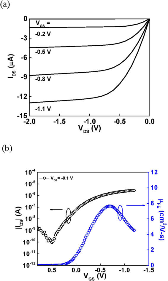
(a) IDS-VDS characteristics and (b) |IDS|-VGS and μFE-VGS characteristics of Ni/SnOx/HfO2/TaN TFTs under an Ar/O2 = 1.0, where the SnOx was formed by reactive sputter from a Sn target.
The reactive sputtering from a Sn target is the crucial technique to reach high hole mobility. Figure 2(a) and (b) show the device characteristics of HfO2/SnOx p-TFTs, where the SnOx was formed by directly sputtering from a SnO target. A low hole μFE of 0.83 cm2/Vs, a poor SS of 430 mV/dec, and a small ION/IOFF of 1.2 × 10³ were measured. Even poor μFE value was measured at annealing temperature higher than 200 °C. The high temperature is needed to anneal out the sputtering damage by energetic ions. But the annealing temperature higher than 200 °C cannot be applied to SnO device, because the SnO will translate to low mobility Sn3O4 and SnO2 at high temperatures24,25.
Figure 2.
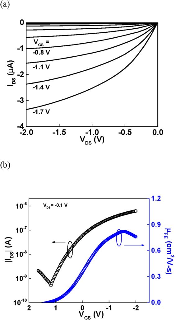
(a) IDS-VDS characteristics and (b) |IDS|-VGS and μFE-VGS characteristics of Ni/SnOx/HfO2/TaN TFTs, where the SnOx was formed by sputter directly from a SnO target.
We have further performed the material analysis to understand the large device performance difference between sputtering from the Sn and SnO targets. Figure 3(a) shows the structure of fabricated Ni/SnOx/HfO2 device. From the cross-sectional transmission electron microscopy (TEM), the SnOx active layer on HfO2 has a thickness of 12 nm. The microscopic structure of SnOx was analyzed by X-ray diffraction (XRD) as shown in Fig. 3(b). For SnOx formed by reactive sputtering from a Sn target, a mixture of major tetragonal α-SnO phase and small amount of β-Sn phase is observed that was caused by the incomplete Sn oxidation26,27. In contrast, only a pure α-SnO phase was found from the SnO target. The atomic composition of SnOx in p-TFT are further characterized by X-ray photoelectron spectroscopy (XPS) in Fig. 3(c). The de-convoluted spectra in both cases show a major Sn2+ peak with tiny Sn4+ and Sn° peaks, although the later ones are smaller for directly sputtered SnO than those from reactive sputtering of a Sn target. Therefore, the SnOx by sputtering from a SnO target gives better material quality. Nevertheless, the μFE is significantly lower than that from the reactive Sn target. The potential reason may be related to the sputter damage from the SnO target, which is difficult to be detected by XRD and XPS analysis. Unfortunately such damage cannot be annealed out because of the limited process temperature of SnO, which can react as scattering centers to low the mobility. The other possibility to reach high mobility may be related to the multi-phonon assisted tunneling28 via small amount of metallic Sn in SnO. This is also associated with the lower off-current in reactive sputtered SnO device than that formed by sputtering from the SnO target. Further theoretical analysis will be required to understand the role of metallic Sn inside SnO. Nevertheless, the metallic Sn is difficult to form by sputtering from the SnO target.
Figure 3.
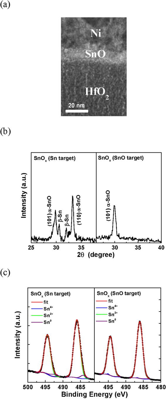
(a) TEM, (b) XRD, and (c) The Sn 3d XPS analysis of SnOx formed from Sn and SnO targets.
It is crucial to notice that the measured hole μFE is the highest value among oxide semiconductors. We further perform the first principle quantum-mechanical calculations on SnO and the other potential candidate of Cu2O (Figures S1 and S2). The structures of both SnO and Cu2O semiconductors were obtained using local density approximation plus U (LDA + U) method with appropriate Up and Ud value. The good accuracy is supported by the calculated band structure of Cu2O; a direct 2.1 eV bandgap and cubic structure were obtained, agreeing well with experiments14,29,30. Both light hole and heavy hole bands were found in Cu2O that are typical for most major semiconductors of Si, Ge, GaAs, InP, InAs etc. Besides, the density of state (DOS) of heavy hole band is considerably higher than that of light hole band to cause the low hole mobility. In sharp contrast, the SnO only has a single hole band, leading to the high hole μFE. The calculated DOS of SnO and Cu2O are further shown in Fig. 4. The Cu2O has much higher DOS than SnO due to its heavy hole bands. For Cu2O, the d-orbital holes have complex intra-atomic hybridization between d and s, p states that lowers the hole mobility. This is also applied for most oxide semiconductors to result in a low hole mobility31–33. In sharp contrast, the Sn 5s orbital is occupied and exhibits a s-p coupling with the O 2p ligand orbitals, unlike the p-d interaction of the d10 Cu2O. The delocalized character of the 5s states leads to a strong valence band dispersion and small hole effective masses in SnO (Figure S3). The SnO has much smaller hole effective mass than Cu2O and other major semiconductors of Si, Ge, GaAs, InP, InGaAs etc. This is the extremely unique merit of SnO p-type transistor to reach high hole mobility.
Figure 4.

DOS distribution of SnO and Cu2O, where d and s, p states hybridization is found for Cu2O.
Table 1 compares the device performance of various TFTs. For p-TFTs, the SnO device has good hole μFE, SS, and ION/IOFF, which is supported from the small effective mass and single band without heavy hole band. The low VD operation is important to lower AC power consumption.
Table 1.
The device performance of various TFTs.
| Channel Materials | Channel layer thickness (nm) | Gate Insulator Materials | SS (V/decade) | μEF (cm2/V·s) | ION/IOFF | Operating Voltage (V) |
|---|---|---|---|---|---|---|
| NiO [15] | 30 | SiO2 | — | 5.2 | ~103 | −100 |
| CuxO [19] | — | ScOx | ~0.4 | 0.8 | ~105 | −3 |
| SnO [20] | 15 | SiO2 | 0.55 | 3.3 | 104 | −3 |
| SnO [25] | 27 | SiO2 | 0.24 | 1.4 | ~104 | −100 |
| This Work SnO | 12 | HfO2 | 0.14 | 7.6 | 3 × 10⁴ | −1.2 |
In conclusion, record high hole mobility of SnO p-TFT was realized. The superb device performance, simple process, and low-cost material make SnO the excellent candidate for next generation ultra-low power display devices and 3D brain-mimicking IC10,13.
Methods
The bottom-gate TFTs were fabricated on a 500-nm-thick SiO2 layer over a Si substrate. A 60-nm TaN was first deposited through reactive sputtering and patterned as the bottom gate electrode. Subsequently, gate dielectric of 40-nm-thick high-κ HfO2 was deposited through physical vapor deposition (PVD) and annealed at 400 °C. Then a 12 nm SnOx was deposited by sputtering in an Ar/O2 mixture from a Sn target, under a DC power of 50 W and a pressure of 7.6 mTorr. Alternatively, the SnOx was deposited by RF sputtering from a SnOx target in the Ar/O2 ambient, under a power of 200 W and a pressure of 7.6 mTorr. Then both the SnO films were subjected to post-deposition annealing at 200 °C in N2 ambient. Finally, the Ni was deposited to form source-drain electrodes. The gate length and width were 50 and 500 μm, respectively. The electrical characteristics of the fabricated devices were measured using an HP4155B parameter analyzer and a probe station. The SnO film was analyzed by transmission electron microscopy (TEM), X-ray diffraction (XRD), and X-ray photoelectron spectroscopy (XPS). The XPS spectra were measured with a PHI 5000 VersaProbe system (ULVAC-PHI, Chigasaki) using a microfocused (100 µm, 25 W) Al X-ray beam. Cross section TEM images of devices were obtained from high resolution transmission electron microscope (JEOL 2010F, USA). The first principle quantum-mechanical calculation was applied to compute the theoretical structural and electrical properties of SnO and Cu2O, using Cambridge Sequential Total Energy Package code (Materials Studio 8.0) with generalized gradient approximation (GGA) and local-density approximations plus Hubbard potential U (LDA + U) method.
Electronic supplementary material
Acknowledgements
The publication of this paper was supported in part by Ministry of Science and Technology of Taiwan. We would like to thank the computing time support from National Taiwan University of Science & Technology and National Center for High-performance Computing. The results of this research have important financial interests for both Display and ultra-low power 3D IC.
Author Contributions
C.W. Shih did the experiments; Albert Chin wrote the main manuscript text; C. Fu Lu and W.F. Su did the quantum-mechanical calculations. All authors reviewed the manuscript.
Competing Interests
The authors declare that they have no competing interests.
Footnotes
Electronic supplementary material
Supplementary information accompanies this paper at 10.1038/s41598-017-17066-x.
Publisher's note: Springer Nature remains neutral with regard to jurisdictional claims in published maps and institutional affiliations.
References
- 1.Fortunato EMC, et al. Fully transparent ZnO thin-film transistor produced at room temperature. Adv. Mater. 2005;17:590. doi: 10.1002/adma.200400368. [DOI] [Google Scholar]
- 2.Zan HW, Yeh CC, Meng HF, Tsai CC, Chen LH. Achieving high field-effect mobility in amorphous indium-gallium-zinc oxide by capping a strong reduction layer. Adv. Mater. 2012;24:3509. doi: 10.1002/adma.201200683. [DOI] [PubMed] [Google Scholar]
- 3.Nomura K, et al. Thin-film transistor fabricated in single-crystalline transparent oxide semiconductor. Science. 2003;300:1269. doi: 10.1126/science.1083212. [DOI] [PubMed] [Google Scholar]
- 4.Suresh, A., Wellenius, P. & Muth, J. F. High performance transparent thin film transistors based on indium gallium zinc oxide as the channel material. IEDM Tech. Dig. 587 (2007).
- 5.Kim, S. I. et al. High performance oxide thin film transistors with double active layers. IEDM Tech. Dig. 73 (2008).
- 6.Kim, T. S. et al. High Performance gallium-zinc oxynitride thin film transistors for next-generation display applications. IEDM Tech. Dig. 660 (2013).
- 7.Lee E, et al. Nanocrystalline ZnON; High mobility and low band gap semiconductor material for high performance switch transistor and image sensor application. Scientific Reports. 2014;4:4948. doi: 10.1038/srep04948. [DOI] [PMC free article] [PubMed] [Google Scholar]
- 8.Bak JY, et al. Origin of degradation phenomenon under drain bias stress for oxide thin film transistors using IGZO and IGO channel layers. Scientific Reports. 2015;5:7884. doi: 10.1038/srep07884. [DOI] [PMC free article] [PubMed] [Google Scholar]
- 9.Park, J. C. et al. High performance amorphous oxide thin film transistors with self-aligned top-gate structure. IEDM Tech. Dig. 191 (2009).
- 10.Shih, C. W., Chin, A., Lu, C. F. & Yi, S. H. Extremely high mobility ultra-thin metal-oxide with ns2np2 configuration. IEDM Tech. Dig. 145 (2015).
- 11.Shih CW, Chin A, Lu CF, Su WF. Remarkably high mobility ultra-thin-film metal-oxide transistor with strongly overlapped orbitals. Sci. Rep. 2016;6:19023. doi: 10.1038/srep19023. [DOI] [PMC free article] [PubMed] [Google Scholar]
- 12.Shih CW, Chin A. New material transistor with record-high field-effect mobility among wide-band-gap semiconductors. ACS Appl. Mater. Interfaces. 2016;8:19187. doi: 10.1021/acsami.6b04332. [DOI] [PubMed] [Google Scholar]
- 13.Shih CW, Chin A. Remarkably High mobility thin-film transistor on flexible substrate by novel passivation material. Scientific Reports. 2017;7:1147. doi: 10.1038/s41598-017-01231-3. [DOI] [PMC free article] [PubMed] [Google Scholar]
- 14.Pattanasattayavong P, Thomas S, Adamopoulos G, McLachlan MA, Anthopoulos TD. P-channel thin-film transistors based on spray-coated Cu2O films. Appl. Phys. Lett. 2013;102:163505. doi: 10.1063/1.4803085. [DOI] [Google Scholar]
- 15.Jiang J, Wang X, Zhang Q, Li J, Zhang X. Thermal oxidation of Ni films for p-type thin-film transistors. Phys. Chem. Chem. Phys. 2013;15:6875. doi: 10.1039/c3cp50197c. [DOI] [PubMed] [Google Scholar]
- 16.Lin T, Li X, Jang J. High performance p-type NiOX thin-film transistor by Sn doping. Appl. Phys. Lett. 2016;108:233503. doi: 10.1063/1.4953222. [DOI] [Google Scholar]
- 17.Ohshima, H. & Morozumi, S. Future trends for TFT integrated circuits on glass substrates. IEDM Tech. Dig. 157 (1989).
- 18.Oana, Y. Current and future technology of low-temperature poly-Si TFT-LCDs. J. SID. 169 (2001).
- 19.Liu A, et al. Water-induced scandium oxide dielectric for low-operating voltage n- and p-type metal-oxide thin-film transistors. Adv. Funct. Mater. 2015;25:7180. doi: 10.1002/adfm.201502612. [DOI] [Google Scholar]
- 20.Zhong CW, Lin HC, Liu KC, Huang TY. Improving electrical performances of p-type SnO thin-film transistors using double-gated structure. IEEE Electron Device Lett. 2015;36:1053. doi: 10.1109/LED.2015.2465144. [DOI] [Google Scholar]
- 21.Liang LY, et al. Ambipolar inverters using SnO thin-film transistors with balanced electron and hole mobilities. Appl. Phys. Lett. 2012;100:263502. doi: 10.1063/1.4731271. [DOI] [Google Scholar]
- 22.Nomura K, Kamiya T, Hosono H. Ambipolar oxide thin-film transistor. Adv. Mater. 2011;23:3431. doi: 10.1002/adma.201101410. [DOI] [PubMed] [Google Scholar]
- 23.Wang, H. et al. Large-scale 2D electronics based on single-layer MoS2 grown by chemical vapor deposition. IEDM Tech. Dig. 88 (2012).
- 24.Hosono H, Ogo Y, Yanagi H, Kamiya T. Bipolar conduction in SnO thin films. Electrochem. Solid-State Lett. 2011;14:H13. doi: 10.1149/1.3505288. [DOI] [Google Scholar]
- 25.Li Y, et al. Extremely sensitive dependence of SnOx film properties on sputtering power. Scientific Reports. 2016;6:36183. doi: 10.1038/srep36183. [DOI] [PMC free article] [PubMed] [Google Scholar]
- 26.Luo, H., Liang, L. Y., Cao, H. T., Liu, Z. M. & Zhuge, F. Structural, chemical, optical, and electrical evolution of SnOx films deposited by reactive rf magnetron sputtering. ACS Appl. Mater. Interfaces4, 5673 (2012). [DOI] [PubMed]
- 27.Wang Z, et al. Transparent SnO–SnO2 p–n junction diodes for electronic and sensing applications. Adv. Mater. Interfaces. 2015;2:1500374. doi: 10.1002/admi.201500374. [DOI] [Google Scholar]
- 28.Shaposhnikov AV, Perevalov TV, Gritsenko VA, Cheng CH, Chin A. Mechanism of GeO2 resistive switching based on the multi-phonon assisted tunneling between traps. Appl. Phys. Lett. 2012;100:243506. doi: 10.1063/1.4729589. [DOI] [Google Scholar]
- 29.Nakano Y, Saeki S, Morikawa T. Optical bandgap widening of p-type Cu2O films by nitrogen doping. Appl. Phys. Lett. 2009;94:022111. doi: 10.1063/1.3072804. [DOI] [Google Scholar]
- 30.Figueiredo V, et al. p-Type CuxO films deposited at room temperature for thin-film transistors. J. Display Technol. 2012;8:1. doi: 10.1109/JDT.2011.2170153. [DOI] [Google Scholar]
- 31.Meng J, Jena P, Vail JM. Hole trapping in LixNi1-xO. J. Phys.: Condens. Matter. 1990;2:10371. [Google Scholar]
- 32.Kamiya T, Hosono H. Material characteristics and applications of transparent amorphous oxide semiconductors. NPG Asia Mater. 2010;2:15. doi: 10.1038/asiamat.2010.5. [DOI] [Google Scholar]
- 33.Granato DB, Caraveo-Frescas JA, Alshareef HN, Schwingenschlogl U. Enhancement of p-type mobility in tin monoxide by native defects. Appl. Phys. Lett. 2013;102:212105. doi: 10.1063/1.4808382. [DOI] [Google Scholar]
Associated Data
This section collects any data citations, data availability statements, or supplementary materials included in this article.