Abstract
The equilibrium optical phonons of graphene are well characterized in terms of anharmonicity and electron–phonon interactions; however, their non-equilibrium properties in the presence of hot charge carriers are still not fully explored. Here we study the Raman spectrum of graphene under ultrafast laser excitation with 3 ps pulses, which trade off between impulsive stimulation and spectral resolution. We localize energy into hot carriers, generating non-equilibrium temperatures in the ~1700–3100 K range, far exceeding that of the phonon bath, while simultaneously detecting the Raman response. The linewidths of both G and 2D peaks show an increase as function of the electronic temperature. We explain this as a result of the Dirac cones’ broadening and electron–phonon scattering in the highly excited transient regime, important for the emerging field of graphene-based photonics and optoelectronics.
Non-equilibrium ultrafast processes in graphene entail relaxation pathways involving electron–electron and electron–phonon scattering events. Here, the authors probe graphene optical phonons at high electronic temperatures by means of Raman spectroscopy under pulsed excitation
Introduction
The distribution of charge carriers has a pivotal role in determining fundamental features of condensed matter systems, such as mobility, electrical conductivity, spin-related effects, transport, and optical properties. Understanding how these proprieties can be affected and, ultimately, manipulated by external perturbations is important for technological applications in diverse areas, ranging from electronics to spintronics, optoelectronics and photonics1–3.
The current picture of ultrafast light interaction with single-layer graphene (SLG) can be summarized as follows4. Absorbed photons create optically excited electron–hole (e–h) pairs. The subsequent relaxation towards thermal equilibrium occurs in three steps. Ultrafast electron–electron (e–e) scattering generates a hot Fermi–Dirac distribution within the first tens fs5. The distribution then relaxes due to scattering with optical phonons (ph; electron–phonon (e–ph) coupling), equilibrating within a few hundred fs6,7. Finally, anharmonic decay into acoustic modes establishes thermodynamic equilibrium on the ps timescale8–10.
Raman spectroscopy is one of the most used characterization techniques in carbon science and technology11. The measurement of the Raman spectrum of graphene12 triggered a substantial effort to understand phonons, e–ph, magneto–ph, and e–e interactions in graphene, as well as the influence of the number and orientation of layers, electric or magnetic fields, strain, doping, disorder, quality and types of edges, and functional groups13–15. The Raman spectra of SLG and few layer graphene (FLG) consist of two fundamentally different sets of peaks. Those, such as D, G, 2D, present also in SLG, and due to in-plane vibrations12, and others, such as the shear (C) modes16 and the layer breathing modes17,18 due to relative motions of the planes themselves, either perpendicular or parallel to their normal. The G peak corresponds to the high frequency E2g phonon at Γ. The D peak is due to the breathing modes of six-atom rings, and requires a defect for its activation19–21. It originates from transverse optical (TO) phonons around the Brillouin Zone edge K[19], it is active by double resonance (DR)[20] and, due to a Kohn Anomaly at K[22], it is dispersive with excitation energy. The 2D peak is the D overtone and originates from a process where momentum conservation is fulfilled by two phonons with opposite wavevectors. It is always present since no defects are required for this process12.
Raman spectroscopy is usually performed under continuous wave (CW) excitation, therefore probing samples in thermodynamic equilibrium. The fast e–e and e–ph non-radiative recombination channels establish equilibrium conditions between charge carriers and lattice, preventing the study of the vibrational response in presence of an hot e–h population. Using an average power comparable to CW illumination (a few mW), ultrafast optical excitation can provide large fluences (~1−15 J m−2 at MHz repetition rates) over sufficiently short timescales (0.1–10 ps) to impulsively generate a strongly out-of-equilibrium distributions of hot e–h pairs4,8,23,24. The potential implications of coupled e and ph dynamics for optoelectronics were discussed for nanoelectronic devices based on CW excitation25–29. However, understanding the impact of transient photoinduced carrier temperatures on the colder SLG ph bath is important for mastering out of equilibrium e–ph scattering, critical for photonics applications driven by carrier relaxation, such as ultrafast lasers30, detectors1,3 and modulators31. E.g, SLG can be used as a much broader-band alternative to semiconductors saturable absorbers30, for mode-locking and Q switching1,30.
Here we characterize the SLG optical ph at high electronic temperature, Te, by performing Raman spectroscopy under pulsed excitation. We use a 3 ps pulse to achieve a trade-off between the narrow excitation bandwidth required for spectral resolution 10 cm−1, being v[Hz] the laser frequency and c the speed of light, a condition met under CW excitation) and a pulse duration, δt, sufficiently short (δt ≤ 10 ps, achieved using ultrafast laser sources) to generate an highly excited carrier distribution over the equilibrium ph population, being those two quantities Fourier conjugates32 . This allows us to determine the dependence of both ph frequency and dephasing time on Te, which we explain by a broadening of the Dirac cones.
Results
Hot photoluminescence
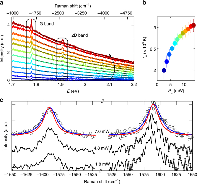
Figure 1a plots a sequence of anti-Stokes (AS) Raman spectra of SLG following ultrafast excitation at 1.58 eV, as a function of excitation power PL. The broad background stems from hot photoluminescence (PL) due to the inhibition of a full non-radiative recombination under high excitation densities8,26,33,34. This process, absent under CW excitation in pristine SLG35, is due to ultrafast photogeneration of charge carriers in the conduction band, congesting the e–ph decay pathway, which becomes progressively less efficient with increasing fluence. This non-equilibrium PL recalls the gray body emission and can be in first approximation described by Planck’s law:8,26,29,33
| 1 |
where η is the emissivity, defined as the dimensionless ratio of the thermal radiation of the material to the radiation from an ideal black surface at the same temperature as given by the Stefan–Boltzmann law36, τem is the emission time and is the frequency dependent, dimensionless responsivity of our detection chain. Refs8,29,33 reported that, although Eq. 1 does not perfectly reproduce the entire gray body emission, the good agreement on a ~0.5 eV energy window is sufficient to extract Te. By fitting the background of the Raman spectra with Eq. 1 (solid lines in Fig. 1a) we obtain Te as a function of PL. Figure 1b shows that Te can reach up to 3100 K under our pulsed excitation conditions.
Fig. 1.
Spectral response of SLG under ultrafast excitation. a AS Raman spectra under ultrafast excitation for laser powers increasing along the arrow direction. The PL-dependent background is fitted by thermal emission (Eq. 1, black lines) resulting in Te in the 1700–3100K range. b Te as a function of PL. Error bars represent the 95% confidence bounds of the best fit. c Background subtracted, AS and S G peak (in black, normalized to the corresponding S maximum) measured as function of PL in the range mW (corresponding to K). Three representative PL values are shown. Best fits of the G peak (blue line), obtained as a convolution of a Lorentzian (red line) with the IRF are also reported for the largest PL value
An upper estimate for the lattice temperature, T1, can be derived assuming a full thermalization of the optical energy between vibrational and electronic degrees of freedom, i.e., evaluating the local equilibrium temperature, Teq, by a specific heat argument (see Methods). We get Teq(Pmax) ~ 680 K at the maximum excitation power, Pmax = 13.5 mW. This is well below the corresponding Te, indicating an out-of-equilibrium distribution of charge carriers. Thus, over our 3 ps observation timescale, T1 is well below Teq.
Out of equilibrium Raman response
Figure 1c plots the AS and S G peaks, together with fits by Lorentzians (blue lines) convoluted with the laser bandwidth (~9.5 cm−1) and spectrometer resolution (~6 cm−1), which determine the instrumental response function, IRF (see Methods). The S data have a larger noise due to a more critical background subtraction, which also requires a wider accessible spectral range (see Methods). For this reason, we will focus on the AS spectral region, with an higher spectrometer resolution (1.2 cm−1), Fig. 2. We obtain a full width at half maximum of the G peak, FWHM(G) ~21 cm−1, larger than the CW one (~12.7 cm−1). Similarly, we get FWHM(2D) ~50–60 cm−1 over our PL range, instead of FWHM(2D) ~29 cm−1 as measured on the same sample under CW excitation. To understand the origin of such large FWHM(G) andFWHM(2D) in pulsed excitation, we first consider the excitation power dependence of the SLG Raman response in the 1.53–13.5 mW range (the lower bound is defined by the detection capability of our setup). This shows that the position of the G peak, Pos(G), is significantly blueshifted (as reported for graphite in ref23.), while the position of the 2D peak, Pos(2D), is close to that measured under CW excitation, and both FWHM(G) and FWHM(2D) increase with PL. Performing the same experiment on Si proves that the observed peaks broadening is not limited by our IRF (see Methods). Moreover, even the low resolution S data of the G band, collected in the range 1.8–7.0 mW (a selection is shown in Fig. 1c), display a broadening ((8 ± 4)10−3 cm−1 K−1) and upshift ((2.8 ± 1.8)10−3 cm−1 K−1), compatible with that of the high-resolution AS measurements (Fig. 3d, e) (7.4 ± 0.5)10−3 cm−1 K−1 and (3.2 ± 0.2)10−3 cm−1 K−1.
Fig. 2.
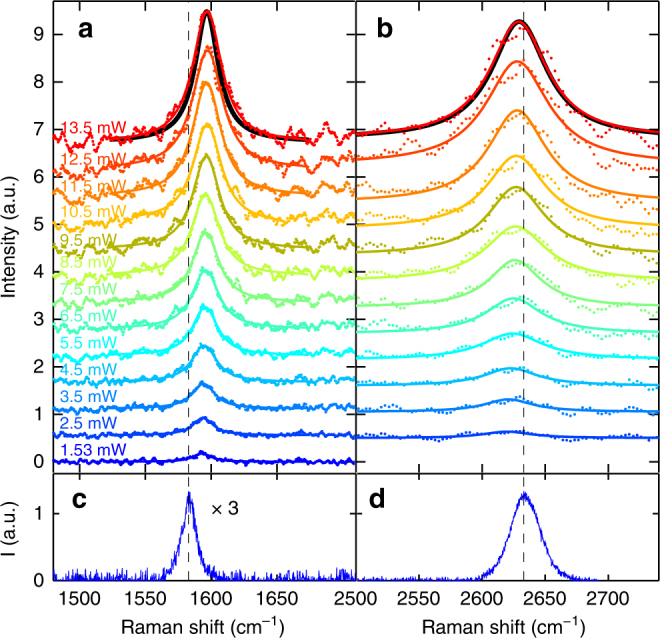
Raman spectra at different laser power. a AS G and b 2D peak as function of PL. (dots) Experimental data. (Lines) fitted Lorentzians convoluted with the spectral profile of the excitation pulse. The vertical dashed lines are the equilibrium, RT, Pos(G) and Pos(2D). c RT CW S G and d 2D peaks. The CW 2D is shifted by 5.4 cm−1 for comparison with the AS ps-Raman, see Methods. The relative calibration accuracy is ∼2 cm−1
Fig. 3.
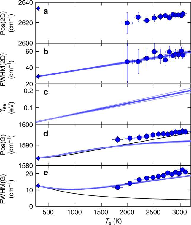
Comparison between theory and experiments. a Pos(2D), b FWHM(2D), d Pos(G), e FWHM(G) as a function of Te for ps-excited Raman spectra. Error bars represent the 95% confidence level in the best fitting procedure. Solid diamonds in a,b,d,e represent the corresponding CW measurements. FWHM(2D) are used to determine the e–e contribution (γee) to the Dirac cones broadening, shown in c (blue lines). Pos(G) and FWHM(G) are compared with theoretical predictions accounting for e–ph interaction in presence of electronic broadening (an additional RT anharmonic damping ∼2 cm−1 10 is included in the calculated FWHM(G)). Black lines are the theoretical predictions for γee = 0 eV, while blue lines take into account an electronic band broadening linearly proportional to Te (γee = αekBTe). From the fit of γee in c, we get = 0.51 cm−1K−1 (thickest blue line). Values of = 0.46,0.55 cm−1K−1, corresponding to 99% confidence boundaries, are also shown (thin light blue lines)
We note that phonons temperature estimates based on the AS/S intensity ratio37,38 are not possible in our case due to two concurring effects. First, SLG’s resonant response to any optical wavelength gives a non trivial wavelength dependent Raman excitation profile, which modifies the Raman intensities with respect to the non-resonant case. Consequently, the AS/S ratio is no longer straightforwardly related to the thermal occupation39. Second, in SLG a S ph may be subsequently annihilated by a correlated AS event. This may result into an extra AS pumping which does not allow to relate AS/S ratio and ph temperature via the thermal occupation factor40. Accordingly, the AS/S ratio approaching one at the largest excitation power in Fig. 1c (black circles) does not necessary imply a large increase of the G phonon temperature.
Discussion
Figure 3 plots Pos(2D), FWHM(2D), Pos(G), FWHM(G) as a function of Te, estimated from the hot-PL. A comparison with CW measurements (633 nm) at room temperature (RT) is also shown (blue diamonds). Under thermodynamic equilibrium, the temperature dependence of the Raman spectrum of SLG is dominated by anharmonicity, which is responsible for mode softening, leading to a redshift of the Raman peaks10,41,42. This differs from our experiments (Fig. 4a–d), in which Pos(G) has an opposite trend (blue shift), and Pos(2D) is nearly Te independent, in agreement with density functional perturbation theory (DFPT) calculations, giving a variation of the 2D peak ΔPos(2D) ~5 cm−1 in the range Te = 300–3000 K (see Methods). This indicates the lack of significant anharmonic effects and suggests a dominant role of e–ph interaction on FWHM(G) and Pos(G), in the presence of a cold phonon bath at constant T1 decoupled from the (large) Te.
Fig. 4.
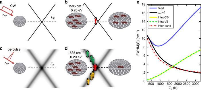
Effect of Dirac cone broadening on Raman process. a CW photoexcitation with mW power does not affect the Dirac cone. b Accordingly, e–h formation induced by e–ph scattering only occurs in presence of resonant ph excitation. c Under ps excitation, with average PL comparable to a, the linear dispersion is smeared by the large kBTe ≈ ħωG = 0.2 eV. d Consequently, e–h formation is enhanced by the increased ph absorption cross section, due to new intra-band processes. e Corresponding contributions to FWHM(G) for the broadened inter-bands and intra-band processes for αekB = 0.51 cm−1 K−1
To derive the temperature dependence of such parameters, we first compute the phonon self-energy , as for refs.22,43,44,
| 2 |
Here is a dimensionless constant, vF is the Fermi velocity, is the upper cutoff of the linear dispersion ε = vF|k|, ma is the carbon atom mass, eV the bare phonon energy, δ is a positive arbitrary small number (< 4 meV), g ~ 12.3 eV is proportional to the e–ph coupling6,22,43,45, z, z′ are the energy integration variables and fF(z − EF) is the Fermi–Dirac distribution with EF the Fermi energy. Although our samples are doped, EF significantly decreases as a function of Te25. Hence, we assume EF = 0 in the following calculations. The two indexes s,s′ = denote the e and h branches, and Ms(z, ε) is the corresponding spectral function, which describes the electronic dispersion.
The self-energy expressed by Eq. 2 renormalizes the phonon Green’s function according to the Dyson’s equation:46
| 3 |
so that ΔPos(G) and FWHM(G) can be written as:
| 4 |
where h is the Planck constant. FWHM(G) can be further simplified since the evaluation of leads to in Eq. 2, so that we get:
| 5 |
In the limit of vanishing broadening of the quasiparticle state, the SLG gapless linear dispersion is represented by the following spectral function:46
| 6 |
This rules the energy conservation in Eq. 5 and allows only transitions between h and e states with energy difference . Thus, we get:22,43,44
| 7 |
where cm−1 10. This value, with the additional ~2 cm−1 contribution arising from anharmonic effects10, is in agreement with the CW measurements at Te = Teq = 300 K (see diamond in Fig. 3e), corresponding to fluences ≪1 J m−2. Eq. 7 also shows that, as Te increases, the conduction band becomes increasingly populated, making the phonon decay channel related to e–h formation progressively less efficient and leading to an increase of the ph decay time (Fig. 4b). This leads to a decrease of FWHM(G) for increasing Te (black solid line in Fig. 3e), in contrast with the experimentally observed increase (blue circles in Fig. 3e).
A more realistic description may be obtained by accounting for the effect of Te on the energy broadening (γe) of the linear dispersion Ms(z,ε), along with the smearing of the Fermi function. γe(z,Te) can be expressed, to a first approximation, as the sum of three terms:47
| 8 |
where γee, γep and γdef are the e–e, e–ph and defect contributions to γe. The only term that significantly depends on Te is γee, while the others depend on the energy z10,44,47–50.
The linear dependence of γee on Te51 can be estimated from its impact on FWHM(2D). The variation of FWHM(2D) with respect to RT can be written as:42
| 9 |
where cm−1 eV−113,52, i.e., the ratio between the ph and Fermi velocity, defined as the slope of the phononic (electronic) dispersion at the ph (e) momentum corresponding to a given excitation laser energy hνlaser13. Since the DR process responsible for the 2D peak involves the creation of e–h pairs at energy hνlaser/2, the change of FWHM(2D) allows us to estimate the variation of γe at eV. Then, γep and γdef, both proportional to z (γep,γdef ∝ z), will give an additional constant contribution to FWHM(2D), but not to its variation with Te. Our data support the predicted51 linear increase of γee with Te, with a dimensionless experimental slope , Fig. 3c.
In order to compute FWHM(G) from Eq. 2, we note that the terms γep and γdef are negligible at the relevant low energy eV . Hence .
The Dirac cone broadening can now be introduced by accounting for γe in the spectral function of Eq. 6:
| 10 |
accordingly, all the processes where the energy difference |sε(k) − s′ε(k′) + ħω0| is less than 2γe (which guarantees the overlap between the spectral functions of the quasiparticles) will now contribute in Eq. 2. Amongst them, those transitions within the same (valence or conduction) band, as shown in Fig. 4d.
The broadened interband contributions still follow, approximately, Eq. 7 (Fig. 4e). However, the Dirac cone broadening gives additional channels for G phonon annihilation by carrier excitation. In particular, intra-band transitions within the Dirac cone are now progressively enabled for increasing Te, as sketched in Fig. 4d. In Fig. 4e the corresponding contributions to FWHM(G) are shown. Calculations in the weak-coupling limit51 suggest that γe(Te) should be suppressed as z → 0, due to phase–space restriction of the Dirac cone dispersion. Our results, however, indicate that this effect should appear at an energy scale smaller than ℏωG/2, as the theory captures the main experimental trends, just based on a z-independent γe(Te).
Critically, the G peak broadening has a different origin from the equilibrium case53. The absence of anharmonicity would imply a FWHM(G) decrease with temperature due to the e–ph mechanism. However, the Dirac cone broadening reverses this trend into a linewidth broadening above Te = 1000K producing, in turn, a dephasing time reduction, corresponding to the experimentally observed FWHM(G) increase. The blue shift of the G peak with temperature is captured by the standard e–ph interaction, beyond possible calibration accuracy. Importantly, the Dirac cone broadening does not significantly affect Pos(G).
In conclusion, we measured the Raman spectrum of SLG with impulsive excitation, in the presence of a distribution of hot charge carriers. Our excitation bandwidth enables us to combine frequency resolution, required to observe the Raman spectra, with short pulse duration, needed to create a significant population of hot carriers. We show that, under these strongly non-equilibrium conditions, the Raman spectrum of graphene cannot be understood based on the standard low fluence picture, and we provide the experimental demonstration of a broadening of the electronic linear dispersion induced by the highly excited carriers. Our results shed light on a peculiar regime of non-equilibrium Raman response, whereby the e–ph interaction is enhanced. This has implications for the understanding of transient charge carrier mobility under photoexcitation, important to study SLG-based optoelectronic and photonic devices27,28, such as broadband light emitters29, transistors and optical gain media54.
Methods
Sample preparation and CW raman characterization
SLG is grown on a 35 μm Cu foil, following the process described in Refs55,56. The substrate is heated to 1000 °C and annealed in hydrogen (H2, 20 sccm) for 30 min. Then, 5 sccm of methane (CH4) is let into the chamber for the following 30 min so that the growth can take place55,56. The sample is then cooled back to RT in vacuum (∼1 mTorr) and unloaded from the chamber. The sample is characterized by CW Raman spectroscopy using a Renishaw inVia Spectrometer equipped with a 100× objective. The Raman spectrum measured at 514 nm is shown in Fig. 5 (red curve). This is obtained by removing the non-flat background Cu PL57. The absence of a significant D peak implies negligible defects12,13,21,58. The 2D peak is a single sharp Lorentzian with FWHM(2D) ∼23 cm−1, a signature of SLG12. Pos(G) is ∼1587 cm−1, with FWHM(G) ∼14 cm−1. Pos(2D) is ∼2705 cm−1, while the 2D to G peak area ratio is ∼4.3. SLG is then transferred on glass by a wet method59. Poly-methyl methacrylate (PMMA) is spin coated on the substrate, which is then placed in a solution of ammonium persulfate (APS) and deionized water. Cu is etched55,59, the PMMA membrane with attached SLG is then moved to a beaker with deionized water to remove APS residuals. The membrane is subsequently lifted with the target substrate. After drying, PMMA is removed in acetone leaving SLG on glass. The SLG quality is also monitored after transfer. The Raman spectrum of the substrate shows features in the D and G peak range, convoluted with the spectrum of SLG on glass (blue curve in Fig. 5). A point-to-point subtraction is needed to reveal the SLG features. After transfer, the D peak is still negligible, demonstrating that no significant additional defects are induced by the transfer process. The fitted Raman parameters indicate p doping ∼250 meV50,60.
Fig. 5.
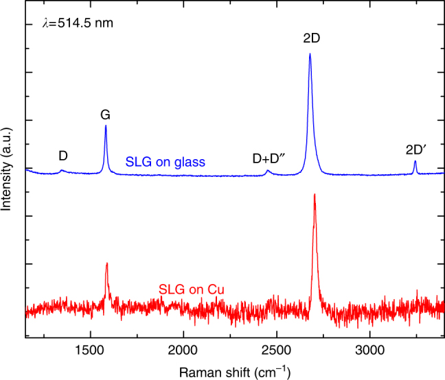
CW Raman spectra of SLG. Raman response of SLG on Cu (red line), and on glass (blue line) after the transfer from Cu. In the latter case, the substrate spectrum is subtracted
Before and after the pulsed laser experiments, equilibrium CW measurements are performed at RT using a micro-Raman setup (LabRAM Infinity). A different energy and momentum of the D phonon is involved, for a given excitation wavelength, in the S or AS processes, due to the phonon dispersion in the DR mechanism61,62. Hence, in order to measure the same D phonon in S and AS, different laser excitations (νlaser) must be used according to 13,63,64. Given our pulsed laser wavelength (783 nm), the corresponding CW excitation would be ∼649.5 nm. Hence, we use a 632.8 nm He-Ne source, accounting for the small residual wavelength mismatch by scaling the phonon frequency as 13.
Pulsed raman measurements
The ps-Raman apparatus is based on a mode-locked Er:fiber amplified laser at ∼1550 nm, producing 90fs pulses at a repetition rate RR = 40 MHz. Using second-harmonic generation in a 1 cm periodically poled Lithium Niobate crystal65, we obtain 3 ps pulses at 783 nm with a ∼9.5 cm−1 bandwidth. The beam is focused on SLG through a slightly underfilled 20× objective (NA = 0.4), resulting in a focal diameter D = 5.7 μm. Back-scattered light is collected by the same objective, separated with a dichroic filter from the incident beam and sent to a spectrometer (with a resolution ~0.028 nm/pixel corresponding to ~1.2 cm−1). The overall IRF, therefore, is dominated by the additional contribution induced by the finite excitation pulse bandwidth. Hence, in order to extract the FWHM of the Raman peaks, our data are fitted convolving a Lorentzian with the spectral profile of the laser excitation.
When using ultrafast pulses, a non-linear PL is seen in SLG8. Such an effect is particularly intense for the S spectral range34,66. The S signal in Fig. 1c is obtained as the difference spectrum of two measurements with excitation frequencies offset by ∼130 cm−1, resulting in PL suppression. The background subtraction requires in this case a wider spectral range, at the expenses of spectrometer resolution which is reduced to ~0.13 nm/pixel, corresponding to ∼6 cm−1, as additional contribution to the IRF. Although this procedure allows to isolate the S Raman peaks, the resulting noise level is worse than for AS. For this reason we mostly focus on the AS features.
To verify that the observed peaks broadening is not limited by our IRF, we perform the same experiment on a Si substrate (Fig. 6a). For this we retrieve, after deconvolution of the IRF, the same Raman linewidth measured in the CW excitation regime (Fig. 6a). The FWHM of the Si optical phonon is independent of PL, in contrast with the well-defined dependence on PL observed in SLG, Fig. 6b.
Fig. 6.
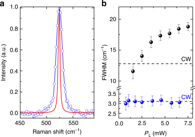
Raman response of Si for pulsed laser excitation. a Raman spectrum of Si measured for ultrafast laser excitation and 6.6 mW average power. (blue line) Lorentzian fit. (red line) laser bandwidth deconvoluted spectrum. b FWHM(Si) as a function of PL (blue symbols) does not show any deviation from the CW FWHM(Si) (dashed blue line). FWHM(G) under the same excitation conditions (black symbols) deviates from the CW regime (dashed black line). Error bars represent the 95% confidence level of the best fit of the Si (a) and SLG (G band) peaks
Estimate of Teq
Photoexcitation of SLG induces an excess of energy in the form of heat per unit area, Q, that can be expressed as:
| 11 |
where A = 2.3% is the SLG absorption, approximated to the undoped case67, is the waist of focused beam and RR = 40 MHz is the repetition rate of the excitation laser. The induced Teq can be derived based on two assumptions: (i) in our ps timescale the energy absorbed in the focal region does not diffuse laterally, (ii) the energy is equally distributed on each degree of freedom (electrons, optical and acoustic ph). Then, Q can be described as:
| 12 |
where C(T) is the SLG T-dependent specific heat. In the 300–700 K range, C(T) can be described as:68 C(T) = aT + b, where a = 1.35×10⁻⁶J K−2 m−2 and b = 1.35×10⁻⁴J K−1 m−2. Therefore, considering Eqs. 11,12, for PL = Pmax = 13.5 mW, we get K, well below the corresponding Te, indicating an out-of-equilibrium condition (Tl < Teq < Te). Any contributions from the substrate and taking into account for the heat profile would contribute in reducing even further Tl estimation.
Estimate of Pos(2D) as a function of Te
We perform calculations within the local density approximation in DFPT69,70. We use the experimental lattice parameter 2.46 Å71 and plane waves (45 Ry cutoff), within a norm-conserving pseudopotential approach70. The electronic levels are occupied with a finite fictitious Te with a Fermi–Dirac distribution, and we sample a Brillouin Zone with a 160 × 160 × 1 mesh. This does not take into account anharmonic effects, assuming Tl = 300K. Figure 7 shows a weak ΔPos(2D) ∼5 cm−1 in the range Te = 300–3000 K. In equilibrium, Tl = Te would induce a non-negligible anharmonicity72, which would lead to a Pos(2D) softening: ΔPos(2D)/ΔTeq ≈ −0.05 cm−1 K−1. The weak dependence ΔPos(2D)(PL) (blue circles in Fig. 7) rules out a dominant anharmonicity contribution and, consequently, Tl = Te. The minor disagreement with DFPT suggests a Tl slightly larger than RT, but definitely smaller than Teq.
Fig. 7.
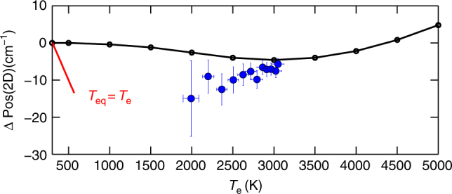
Temperature dependence of Pos(2D). Pos(2D), relative to the RT CW measurement, as a function of Te. Black line: DFPT; blue circles: experimental data with pulsed excitation. Red line: T-dependent CW measurement in thermal equilibrium (Te = Tl = Teq) from ref.72. The error bars represent the 95% of confidence level, as in Fig. 3
Data availability
All relevant data are available from the authors.
Acknowledgements
We acknowledge funding from the Graphene Flagship, ERC Grant Hetero2D, EPSRC Grants EP/K01711X/1, EP/K017144/1, EP/N010345/1, EP/L016087/1 and MAECI under the Italia-India collaborative project SuperTop-PGR04879.
Author contributions
T.S. led the research project, conceived with G.C., F.M. and A.C.F.; C.Fe., A.V., and T.S. designed and built the pulsed Raman setup; C.Fe. and A.V. performed the out of equilibrium Raman experiments, with contribution from M.M.; C.Fa., P.P., D.D.F., U.S., A.K.O., and D.Y. performed the equilibrium CW Raman experiment; L.B. and F.M. developed the modeling and carried out the numerical simulations, with contributions from A.V.; D.D.F., U.S., A.K.O., and D.Y. prepared and characterized the samples; C.Fe., A.V., L.B., G.C., F.M., A.C.F., and T.S. interpreted the data and the simulations and wrote the manuscript.
Competing interests
The authors declare no competing financial interests.
Footnotes
C. Ferrante and A. Virga contributed equally to this work.
Publisher's note: Springer Nature remains neutral with regard to jurisdictional claims in published maps and institutional affiliations.
Contributor Information
C. Ferrante, Email: carino.ferrante@roma1.infn.it
T. Scopigno, Email: tullio.scopigno@roma1.infn.it
References
- 1.Bonaccorso F, Sun Z, Hasan T, Ferrari AC. Graphene photonics and optoelectronics. Nat. Photonics. 2010;4:611–622. doi: 10.1038/nphoton.2010.186. [DOI] [Google Scholar]
- 2.Ferrari AC, et al. Science and technology roadmap for graphene, related two-dimensional crystals, and hybrid systems. Nanoscale. 2015;7:4598–4810. doi: 10.1039/C4NR01600A. [DOI] [PubMed] [Google Scholar]
- 3.Koppens FHL, et al. Photodetectors based on graphene, other two-dimensional materials and hybrid systems. Nat. Nanotech. 2014;9:780–793. doi: 10.1038/nnano.2014.215. [DOI] [PubMed] [Google Scholar]
- 4.Brida D, et al. Ultrafast collinear scattering and carrier multiplication in graphene. Nat. Commun. 2013;4:1987. doi: 10.1038/ncomms2987. [DOI] [PubMed] [Google Scholar]
- 5.Tomadin A, Brida D, Cerullo G, Ferrari AC, Polini M. Nonequilibrium dynamics of photoexcited electrons in graphene: Collinear scattering, auger processes, and the impact of screening. Phys. Rev. B. 2013;88:035430. doi: 10.1103/PhysRevB.88.035430. [DOI] [Google Scholar]
- 6.Lazzeri M, Piscanec S, Mauri F, Ferrari AC, Robertson J. Electron transport and hot phonons in carbon nanotubes. Phys. Rev. Lett. 2005;95:236802. doi: 10.1103/PhysRevLett.95.236802. [DOI] [PubMed] [Google Scholar]
- 7.Butscher S, Milde F, Hirtschulz M, Mali E, Knorr A. Hot electron relaxation and phonon dynamics in graphene. Appl. Phys. Lett. 2007;91:203103. doi: 10.1063/1.2809413. [DOI] [Google Scholar]
- 8.Lui CH, Mak KF, Shan J, Heinz TF. Ultrafast photoluminescence from graphene. Phys. Rev. Lett. 2010;105:127404. doi: 10.1103/PhysRevLett.105.127404. [DOI] [PubMed] [Google Scholar]
- 9.Wu S, et al. Hot phonon dynamics in graphene. Nano Lett. 2012;12:5495–5499. doi: 10.1021/nl301997r. [DOI] [PubMed] [Google Scholar]
- 10.Bonini N, Lazzeri M, Marzari N, Mauri F. Phonon anharmonicities in graphite and graphene. Phys. Rev. Lett. 2007;99:176802. doi: 10.1103/PhysRevLett.99.176802. [DOI] [PubMed] [Google Scholar]
- 11.Ferrari AC, Robertson Je. Raman spectroscopy in carbons: from nanotubes to diamond, theme issue. Philos. Trans. R. Soc. Lond. A. 2004;362:2267–2565. [Google Scholar]
- 12.Ferrari AC, et al. Raman spectrum of graphene and graphene layers. Phys. Rev. Lett. 2006;97:187401. doi: 10.1103/PhysRevLett.97.187401. [DOI] [PubMed] [Google Scholar]
- 13.Ferrari AC, Basko DM. Raman spectroscopy as a versatile tool for studying the properties of graphene. Nat. Nanotech. 2013;8:235–246. doi: 10.1038/nnano.2013.46. [DOI] [PubMed] [Google Scholar]
- 14.Malard L, Pimenta M, Dresselhaus G, Dresselhaus M. Raman spectroscopy in graphene. Phys. Rep. 2009;473:51–87. doi: 10.1016/j.physrep.2009.02.003. [DOI] [Google Scholar]
- 15.Froehlicher G, Berciaud S. Raman spectroscopy of electrochemically gated graphene transistors: Geometrical capacitance, electron-phonon, electron-electron, and electron-defect scattering. Phys. Rev. B. 2015;91:205413. doi: 10.1103/PhysRevB.91.205413. [DOI] [Google Scholar]
- 16.Tan PH, et al. The shear mode of multilayer graphene. Nat. Mater. 2012;11:294–300. doi: 10.1038/nmat3245. [DOI] [PubMed] [Google Scholar]
- 17.Sato K, et al. Raman spectra of out-of-plane phonons in bilayer graphene. Phys. Rev. B. 2011;84:035419. doi: 10.1103/PhysRevB.84.035419. [DOI] [Google Scholar]
- 18.Lui CH, et al. Observation of layer-breathing mode vibrations in few-layer graphene through combination raman scattering. Nano Lett. 2012;12:5539–5544. doi: 10.1021/nl302450s. [DOI] [PubMed] [Google Scholar]
- 19.Tuinstra F, Koenig JL. Raman spectrum of graphite. J. Chem. Phys. 1970;53:1126–1130. doi: 10.1063/1.1674108. [DOI] [Google Scholar]
- 20.Thomsen C, Reich S. Double resonant raman scattering in graphite. Phys. Rev. Lett. 2000;85:5214–5217. doi: 10.1103/PhysRevLett.85.5214. [DOI] [PubMed] [Google Scholar]
- 21.Ferrari AC, Robertson J. Interpretation of raman spectra of disordered and amorphous carbon. Phys. Rev. B. 2000;61:14095–14107. doi: 10.1103/PhysRevB.61.14095. [DOI] [Google Scholar]
- 22.Piscanec S, Lazzeri M, Mauri F, Ferrari AC, Robertson J. Kohn anomalies and electron-phonon interactions in graphite. Phys. Rev. Lett. 2004;93:185503. doi: 10.1103/PhysRevLett.93.185503. [DOI] [PubMed] [Google Scholar]
- 23.Yan H, et al. Time-resolved raman spectroscopy of optical phonons in graphite: Phonon anharmonic coupling and anomalous stiffening. Phys. Rev. B. 2009;80:121403. doi: 10.1103/PhysRevB.80.121403. [DOI] [Google Scholar]
- 24.Breusing M, et al. Ultrafast nonequilibrium carrier dynamics in a single graphene layer. Phys. Rev. B. 2011;83:153410. doi: 10.1103/PhysRevB.83.153410. [DOI] [Google Scholar]
- 25.Chae DH, Krauss B, von Klitzing K, Smet JH. Hot phonons in an electrically biased graphene constriction. Nano Lett. 2010;10:466–471. doi: 10.1021/nl903167f. [DOI] [PubMed] [Google Scholar]
- 26.Berciaud S, et al. Electron and optical phonon temperatures in electrically biased graphene. Phys. Rev. Lett. 2010;104:227401. doi: 10.1103/PhysRevLett.104.227401. [DOI] [PubMed] [Google Scholar]
- 27.McKitterick CB, Prober DE, Rooks MJ. Electron-phonon cooling in large monolayer graphene devices. Phys. Rev. B. 2016;93:075410. doi: 10.1103/PhysRevB.93.075410. [DOI] [Google Scholar]
- 28.Mogulkoc A, et al. The role of electron–phonon interaction on the transport properties of graphene based nano-devices. Phys. B. 2014;446:85–91. doi: 10.1016/j.physb.2014.04.034. [DOI] [Google Scholar]
- 29.Kim YD, et al. Bright visible light emission from graphene. Nat. Nano. 2015;10:676–681. doi: 10.1038/nnano.2015.118. [DOI] [PubMed] [Google Scholar]
- 30.Sun Z, et al. Graphene mode-locked ultrafast laser. ACS Nano. 2010;4:803–810. doi: 10.1021/nn901703e. [DOI] [PubMed] [Google Scholar]
- 31.Liu M, et al. A graphene-based broadband optical modulator. Nature. 2011;474:64–67. doi: 10.1038/nature10067. [DOI] [PubMed] [Google Scholar]
- 32.Papoulis, A. The Fourier Integral and Its Applications (Mcgraw-Hill College, New York, 1962).
- 33.Freitag M, Chiu HY, Steiner M, Perebeinos V, Avouris P. Thermal infrared emission from biased graphene. Nat. Nanotech. 2010;5:497–501. doi: 10.1038/nnano.2010.90. [DOI] [PubMed] [Google Scholar]
- 34.Stöhr RJ, Kolesov R, Pflaum J, Wrachtrup J. Fluorescence of laser-created electron-hole plasma in graphene. Phys. Rev. B. 2010;82:121408. doi: 10.1103/PhysRevB.82.121408. [DOI] [Google Scholar]
- 35.Gokus T, et al. Making graphene luminescent by oxygen plasma treatment. ACS Nano. 2009;3:3963–3968. doi: 10.1021/nn9012753. [DOI] [PubMed] [Google Scholar]
- 36.Callen, H. B. Thermodynamics and an Introduction to Thermostatistics (John Wiley & Sons, Inc., New York, 1985).
- 37.Schomacker KT, Champion PM. Investigations of spectral broadening mechanisms in biomolecules: Cytochrome–Âc. J. Chem. Phys. 1986;84:5314–5325. doi: 10.1063/1.449942. [DOI] [Google Scholar]
- 38.Souza Filho AG, et al. Electronic transition energy for an isolated single-wall carbon nanotube obtained by anti-stokes/stokes resonant raman intensity ratio. Phys. Rev. B. 2001;63:241404. doi: 10.1103/PhysRevB.63.241404. [DOI] [Google Scholar]
- 39.Goldstein T, et al. Raman scattering and anomalous stokes–anti-stokes ratio in MoTe atomic layers. Sci. Rep. 2016;6:28024. doi: 10.1038/srep28024. [DOI] [PMC free article] [PubMed] [Google Scholar]
- 40.Parra-Murillo CA, Santos MF, Monken CH, Jorio A. Stokes–anti-Stokes correlation in the inelastic scattering of light by matter and generalization of the bose-einstein population function. Phys. Rev. B. 2016;93:125141. doi: 10.1103/PhysRevB.93.125141. [DOI] [Google Scholar]
- 41.Apostolov AT, Apostolova IN, Wesselinowa JM. Temperature and layer number dependence of the g and 2d phonon energy and damping in graphene. J. Phys. Condens. Matter. 2012;24:235401. doi: 10.1088/0953-8984/24/23/235401. [DOI] [PubMed] [Google Scholar]
- 42.Basko DM. Theory of resonant multiphonon raman scattering in graphene. Phys. Rev. B. 2008;78:125418. doi: 10.1103/PhysRevB.78.125418. [DOI] [Google Scholar]
- 43.Lazzeri M, Mauri F. Nonadiabatic kohn anomaly in a doped graphene monolayer. Phys. Rev. Lett. 2006;97:266407. doi: 10.1103/PhysRevLett.97.266407. [DOI] [PubMed] [Google Scholar]
- 44.Pisana S, et al. Breakdown of the adiabatic born-oppenheimer approximation in graphene. Nat. Mater. 2007;6:198–201. doi: 10.1038/nmat1846. [DOI] [PubMed] [Google Scholar]
- 45.Ferrari AC. Raman spectroscopy of graphene and graphite: Disorder, electron–phonon coupling, doping and nonadiabatic effects. Solid State Commun. 2007;143:47–57. doi: 10.1016/j.ssc.2007.03.052. [DOI] [Google Scholar]
- 46.Ando T. Anomaly of optical phonon in monolayer graphene. J. Phys. Soc. Jpn. 2006;75:124701. doi: 10.1143/JPSJ.75.124701. [DOI] [Google Scholar]
- 47.Venezuela P, Lazzeri M, Mauri F. Theory of double-resonant raman spectra in graphene: Intensity and line shape of defect-induced and two-phonon bands. Phys. Rev. B. 2011;84:035433. doi: 10.1103/PhysRevB.84.035433. [DOI] [Google Scholar]
- 48.Yan J, Zhang Y, Kim P, Pinczuk A. Electric field effect tuning of electron-phonon coupling in graphene. Phys. Rev. Lett. 2007;98:166802. doi: 10.1103/PhysRevLett.98.166802. [DOI] [PubMed] [Google Scholar]
- 49.Neumann C, et al. Raman spectroscopy as probe of nanometre-scale strain variations in graphene. Nat. Commun. 2015;6:8429. doi: 10.1038/ncomms9429. [DOI] [PMC free article] [PubMed] [Google Scholar]
- 50.Basko DM, Piscanec S, Ferrari AC. Electron-electron interactions and doping dependence of the two-phonon raman intensity in graphene. Phys. Rev. B. 2009;80:165413. doi: 10.1103/PhysRevB.80.165413. [DOI] [Google Scholar]
- 51.Schütt M, Ostrovsky PM, Gornyi IV, Mirlin AD. Coulomb interaction in graphene: Relaxation rates and transport. Phys. Rev. B. 2011;83:155441. doi: 10.1103/PhysRevB.83.155441. [DOI] [Google Scholar]
- 52.Vidano R, Fischbach D, Willis L, Loehr T. Observation of raman band shifting with excitation wavelength for carbons and graphites. Solid State Commun. 1981;39:341–344. doi: 10.1016/0038-1098(81)90686-4. [DOI] [Google Scholar]
- 53.Balandin AA, et al. Superior thermal conductivity of single-layer graphene. Nano Lett. 2008;8:902–907. doi: 10.1021/nl0731872. [DOI] [PubMed] [Google Scholar]
- 54.Engel M, et al. Light–matter interaction in a microcavity-controlled graphene transistor. Nat. Commun. 2012;3:906. doi: 10.1038/ncomms1911. [DOI] [PMC free article] [PubMed] [Google Scholar]
- 55.Bae S, et al. Roll-to-roll production of 30-inch graphene films for transparent electrodes. Nat. Nanotech. 2010;5:574–578. doi: 10.1038/nnano.2010.132. [DOI] [PubMed] [Google Scholar]
- 56.Li X, et al. Large-area synthesis of high-quality and uniform graphene films on copper foils. Science. 2009;324:1312–1314. doi: 10.1126/science.1171245. [DOI] [PubMed] [Google Scholar]
- 57.Lagatsky AA, et al. 2m solid-state laser mode-locked by single-layer graphene. Appl. Phys. Lett. 2013;102:013113. doi: 10.1063/1.4773990. [DOI] [Google Scholar]
- 58.Cançado LG, et al. Quantifying defects in graphene via raman spectroscopy at different excitation energies. Nano Lett. 2011;11:3190–3196. doi: 10.1021/nl201432g. [DOI] [PubMed] [Google Scholar]
- 59.Bonaccorso F, et al. Production and processing of graphene and 2d crystals. Mater. Today. 2012;15:564–589. doi: 10.1016/S1369-7021(13)70014-2. [DOI] [Google Scholar]
- 60.Das A, et al. Monitoring dopants by raman scattering in an electrochemically top-gated graphene transistor. Nat. Nanotech. 2008;3:210–215. doi: 10.1038/nnano.2008.67. [DOI] [PubMed] [Google Scholar]
- 61.Baranov, A. V., Bekhterev, A. N., Bobovich, Y. S. & Petrov, V. I. Interpretation of certain characteristics in raman spectra of graphite and glassy carbon. Opt. Spectrosc. 62, 612–616 (1987).
- 62.Thomsen C, Reich S. Double resonant raman scattering in graphite. Phys. Rev. Lett. 2000;85:5214–5217. doi: 10.1103/PhysRevLett.85.5214. [DOI] [PubMed] [Google Scholar]
- 63.Tan P, et al. Probing the phonon dispersion relations of graphite from the double-resonance process of stokes and anti-stokes raman scatterings in multiwalled carbon nanotubes. Phys. Rev. B. 2002;66:245410. doi: 10.1103/PhysRevB.66.245410. [DOI] [Google Scholar]
- 64.Cançado LG, et al. Stokes and anti-stokes double resonance raman scattering in two-dimensional graphite. Phys. Rev. B. 2002;66:035415. doi: 10.1103/PhysRevB.66.035415. [DOI] [Google Scholar]
- 65.Marangoni M, et al. Narrow-bandwidth picosecond pulses by spectral compression of femtosecond pulses in a second-order nonlinear crystal. Opt. Express. 2007;15:8884–8891. doi: 10.1364/OE.15.008884. [DOI] [PubMed] [Google Scholar]
- 66.Liu WT, et al. Nonlinear broadband photoluminescence of graphene induced by femtosecond laser irradiation. Phys. Rev. B. 2010;82:081408. doi: 10.1103/PhysRevB.82.081408. [DOI] [Google Scholar]
- 67.Nair RR, et al. Fine structure constant defines visual transparency of graphene. Science. 2008;320:1308–1308. doi: 10.1126/science.1156965. [DOI] [PubMed] [Google Scholar]
- 68.Pop E, Varshney V, Roy AK. Thermal properties of graphene: Fundamentals and applications. MRS Bull. 2012;37:1273–1281. doi: 10.1557/mrs.2012.203. [DOI] [Google Scholar]
- 69.de Gironcoli S. Lattice dynamics of metals from density-functional perturbation theory. Phys. Rev. B. 1995;51:6773–6776. doi: 10.1103/PhysRevB.51.6773. [DOI] [PubMed] [Google Scholar]
- 70.Giannozzi P, et al. Quantum espresso: a modular and open-source software project for quantum simulations of materials. J. Phys. Condens. Matter. 2009;21:395502. doi: 10.1088/0953-8984/21/39/395502. [DOI] [PubMed] [Google Scholar]
- 71.Wang Y, Panzik JE, Kiefer B, Lee KKM. Crystal structure of graphite under room-temperature compression and decompression. Sci. Rep. 2012;2:520. doi: 10.1038/srep00520. [DOI] [PMC free article] [PubMed] [Google Scholar]
- 72.Nef C, et al. High-yield fabrication of nm-size gaps in monolayer cvd graphene. Nanoscale. 2014;6:7249–7254. doi: 10.1039/C4NR01838A. [DOI] [PubMed] [Google Scholar]
Associated Data
This section collects any data citations, data availability statements, or supplementary materials included in this article.
Data Availability Statement
All relevant data are available from the authors.


