Abstract
The organic charge-transfer (CT) complex dibenzotetrathiafulvalene – 7,7,8,8-tetracyanoquinodimethane (DBTTF-TCNQ) is found to crystallize in two polymorphs when grown by physical vapor transport: the known α-polymorph and a new structure, the β-polymorph. Structural and elemental analysis via selected area electron diffraction (SAED), X-ray photoelectron spectroscopy (XPS), and polarized IR spectroscopy reveal that the complexes have the same stoichiometry with a 1:1 donor:acceptor ratio, but exhibit unique unit cells. The structural variations result in significant differences in the optoelectronic properties of the crystals, as observed in our experiments and electronic-structure calculations. Raman spectroscopy shows that the α-polymorph has a degree of charge transfer of about 0.5e, while the β-polymorph is nearly neutral. Organic field-effect transistors fabricated on these crystals reveal that in the same device structure both polymorphs show ambipolar charge transport, but the α-polymorph exhibits electron-dominant transport while the β-polymorph is hole-dominant. Together, these measurements imply that the transport features result from differing donor-acceptor overlap and consequential varying in frontier molecular orbital mixing, as suggested theoretically for charge-transfer complexes.
Keywords: organic semiconductors, Organic Electronics, charge-transfer complexes, single crystals, polymorphism
Table of Contents Entry
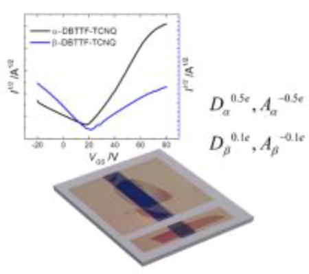
The organic charge-transfer complex DBTTF-TCNQ is found to grow in two polymorphs, both mixed-stack. Their characterization via organic field-effect transistors, XPS, Raman, and IR spectroscopies show that subtle differences in their structure have a large impact on their electrical characteristics and electronic structure. These results support theoretical calculations that discuss the implications of small shifts in donor/acceptor overlap.
1. Introduction
Organic electronic materials are promising for a wide variety of consumer applications due to their compatibility with flexible substrates, their favorable interaction with biological media, and their versatility in generating tailored materials which can be designed and engineered for specific applications. Organic charge-transfer (CT) complexes – multi-component materials in which one molecule acts as an electron donor (D) and another as an electron acceptor (A) – are a class of organic materials with the potential for such controlled design[1–4]. Within the complex, the two species, which tend to be unipolar semiconductors in their pristine form, create a hybrid band structure primarily composed of the donor HOMO (highest occupied molecular orbital) and the acceptor LUMO (lowest unoccupied molecular orbital)[5,6]. The result is a smaller effective bandgap and partial ionicity, which leads to a rich array of optoelectronic behavior that is both fundamentally interesting and technologically relevant. This includes ambipolar semiconductivity, metallic behavior, ferroelectricity, and more[7–16]. Control over the CT complex energetics and properties lies largely in the choice of the D/A parent compounds, but the crystalline packing plays a key role[6]. A clear indicator of this is the existence of several complexes that possess the same donor and acceptor molecules in the same ratio, but show metallic behavior in their segregated stack form and semiconducting behavior in their mixed-stack form[2]. For example, BEDT-TTF – TCNQ (where BEDT-TTF is the donor bis(ethylenedithio)-tetrathiafulvalene and TCNQ is the acceptor 7,7,8,8-tetracyanoquinodimethane) has two metallic phases, both exhibiting a room-temperature electrical conductivity of 10 Ω−1cm−1: one crystallizes in a triclinic (β′) segregated-stack structure and has a degree of charge transfer (ρ) of 0.5e between the D and A (where e is the elementary charge)[17–19], while the other crystallizes in a triclinic (β″) segregated-stack structure and is characterized by a 0.74e degree of charge transfer[20,21]. In contrast, its monoclinic, mixed-stack structure[22] is a semiconductor with seven orders of magnitude lower conductivity and a degree of charge transfer of ρ = 0.1e[18,19].
Similar to monomolecular compounds, the charge transport in a CT complex is dependent on the extent of coupling between the constituent molecules – in this case the D and A molecular orbitals. This, in turn, is governed by the compound’s crystal structure, with both the coupling and the degree of charge transfer changing as a function the molecular overlap of the stacked donor and acceptor molecules[23]. Theoretical studies have suggested that in-stack charge-transport for a mixed-stack CT complex takes place via a superexchange mechanism, where electron (hole) transport occurs in an A-D-A (D-A-D) triad via mixing of the acceptor LUMO with the donor HOMO[5,6,24]. Balanced hole and electron transport is expected when the transport occurs predominantly via the donor HOMO and the acceptor LUMO. If other orbitals are involved in transport, however, electrons and holes exhibit unbalanced charge carrier mobilities, and charge transport can even be unipolar in the most extreme cases[6].
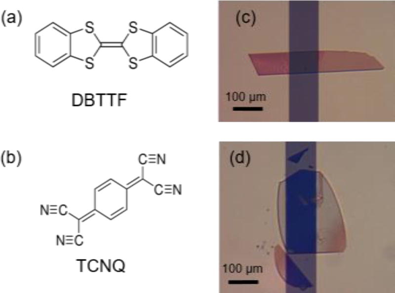
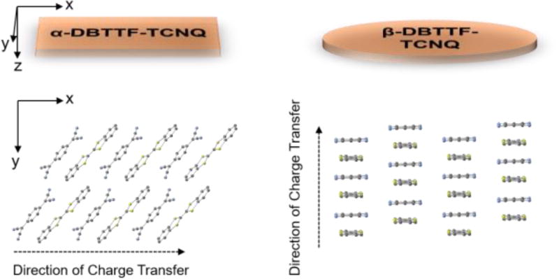
Experimental validation of these theories is difficult due to limited available materials and unavoidable extrinsic factors that participate in the measurement of electrical properties. In this article, we study such effects by exploring the properties of two polymorphs of the CT complex dibenzotetrathiafulvalene – 7,7,8,8-tetracyanoquinodimethane (DBTTF-TCNQ) (Figure 1a, 1b). These form an excellent system for the study of the effect of D/A interactions on the optical properties and charge transport in CT complexes because the constituent molecules are exactly the same, but variations in their molecular packing result in different functionality. We will refer to the known, triclinic polymorph as the α-polymorph[25–27]. Crystals of this structure adopt a rectangular shape (Figure 1c), whereas the crystals of the new, previously-unreported polymorph (which we will call the β-polymorph), are elliptical in shape (Figure 1d). The thin nature of the β-crystals made it impossible to determine its structure by X-ray diffraction (XRD). Therefore, a combination of selected area electron diffraction (SAED), IR and UV-vis absorption spectroscopies was used to confirm the structure of the α-polymorph and estimate the structure of the new polymorph. Density Functional Theory (DFT) calculations allowed us to further refine this crystal structure and compare features of its electronic structure to those of the α-polymorph[5].
Figure 1.
Chemical structure of (a) the donor, DBTTF, and (b) the acceptor, TCNQ. (c) Rectangular α-DBTTF-TCNQ crystal. (d) Elliptical β-DBTTF-TCNQ crystal.
To evaluate the optoelectronic properties of the two polymorphs we incorporated their single crystals in organic field-effect transistors (OFETs). We observed that the differences between the two systems are very subtle, both exhibiting ambipolar-semiconducting electrical properties with gold source/drain contacts. The α-polymorph shows superior electron transport while, in contrast, the β-polymorph exhibits hole dominant transport. Raman spectroscopy suggests that the degree of charge transfer between the D and A molecules in the α-polymorph approaches ρ = 0.5e, whereas the β-polymorph is almost neutral, with ρ = 0.1e. Our in-depth investigations of the structural, optical, and electronic properties of DBTTF-TCNQ crystals provide conclusive evidence of the impact of crystalline packing on the properties of mixed-stack CT complexes and validate the theoretical calculations which predict that the charge transport can lose its balanced nature if other orbitals besides the donor HOMO and the acceptor LUMO participate in charge transport. We propose that the more favorable charge transport pathway for holes in β-DBTTF-TCNQ compared to the α-polymorph is a consequence of varying frontier orbital mixing between the two polymorphs.
2. Results
2.1. Single Crystal Growth of DBTTF-TCNQ
The crystal structure of an organic crystalline solid is mediated by the interplay between van der Waals interactions and dipoles or multipoles (either permanent or induced)[28]. Because of the weak energies of these interactions, variations in growth conditions can result in polymorphism. This is the case for several monomolecular compounds where the structure is dictated by the type of solvent used for crystallization, by temperature, or other growth conditions. To grow single crystals of each DBTTF-TCNQ polymorph, we first prepared the CT crystals by a solution diffusion method. To achieve that, a solution of TCNQ in acetonitrile, saturated at ≈ 60°C, was mixed with a similarly saturated and heated DBTTF solution in xylenes. Needle-like crystals of the α-polymorph precipitated as the solution cooled. Though evidence exists for the crystallization of charge-transfer complexes in different stoichiometries due to varying solvents[29], we were unable to crystallize the β-polymorph from solution. The solution-grown crystals were used as source material to grow flat, thin crystals of both the α- and β- polymorphs by physical vapor transport (PVT)[30–32]. The carrier gas in use here was argon flowing at a rate of 150 mL/min in a tube under a temperature gradient (Figure S1). The source material was heated to 170 °C, and the α- and β- polymorphs crystallized in different regions of the tube, between room-temperature and 45 °C and 40–65 °C, respectively. They were discernable by their shape – α-DBTTF-TCNQ is rectangular, while β-DBTTF-TCNQ is elliptical and very thin (see Figure 1). Growth conditions vary strongly between different furnaces – we note that our growth conditions are different from prior reports on α-DBTTF-TCNQ[31,32] – therefore, a full description of the PVT process is included in the supplementary information.
2.2. Structural Characterization of DBTTF-TCNQ Polymorphs
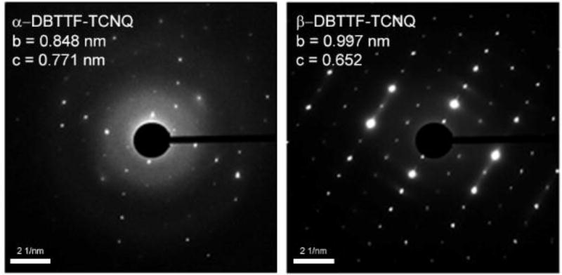
The crystal structure of the α-polymorph was confirmed by X-ray diffraction (XRD). The obtained unit cell parameters coincide with the previously reported ones[26] with a = 7.7576 Å, b = 8.3622 Å, c = 10.400 Å, α = 72.14°, β = 109.77°, and γ = 110.19°. The β-polymorph crystals were extremely thin, and even synchrotron XRD measurements were unsuccessful in determining their structure. Therefore, a combination of SAED, IR spectroscopy, XPS, optical absorbance, and DFT calculations was used to determine the unit cell and orientation of the bulk crystal, evaluate the D:A ratio, and to estimate the crystal structure. The SAED results for the two DBTTF-TCNQ polymorphs are shown in Figure 2. The parameters for the α-polymorph (Figure 2a) are similar to the triclinic unit cell reported by Kobayashi, et al, where the space-group is P1̄[26,27]. Earlier SAED measurements on microrods of DBTTF-TCNQ exhibited a unit cell structure similar to the α-polymorph discussed here[33]. In contrast, the β-polymorph has a distinct unit cell with lattice parameters of b = 0.997 nm, c = 0.652 nm, and an angle of 90° between them, suggesting a monoclinic symmetry (Figure 2b). DFT calculations were performed to obtain additional insight on the packing and electronic structure of the β-polymorph. By using lattice parameters obtained from SAED measurements as an initial input, several crystal structures have been optimized. The most stable structure obtained has the following unit cell parameters: a = 8.83 Å, b = 9.57 Å, c = 6.83 Å, α = 83.59°, β = 84.99°, and γ = 88.54°. This geometric structure was then used for all electronic structure calculations. As SAED measurements suggest that the unit cell of this system could be of a higher than the triclinic symmetry resulting from our calculations, further investigations are needed to fully characterize the β-polymorph. In particular, unit cells containing two or more donor-acceptor pairs should be considered for donor-acceptor crystals with high symmetry, as is suggested by the available experimental data.
Figure 2.
SAED patterns for the α-DBTTF-TCNQ (left panel) and β-DBTTF-TCNQ (right panel). Measured lattice parameters are listed below the corresponding patterns.
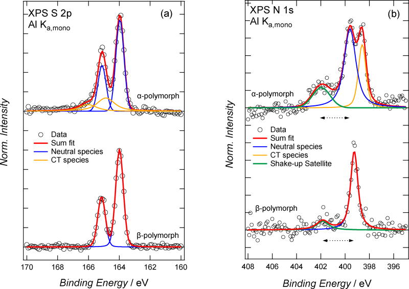
X-ray photoelectron spectroscopy (XPS) identifies and quantifies the chemical composition of the crystals, and can also provide information about the degree of charge transfer between the donor and acceptor in the complex, as we will show in the next section. In this study, we are able to use the S 2p spectra to represent features of the donor moiety because DBTTF is sulfur-containing and TCNQ is not (Figure 3a). Similarly, the N1s spectrum is representative of the acceptor (Figure 3b). Details of the spectral fitting are included in the supplementary materials. Relative sulfur and nitrogen content was estimated by XPS by using the S 2s and N 1s photoemission (PES) lines and correcting by the photoionization cross sections and spectrometer transmission function. The sulfur fraction, [S]/([S]+[N]), is 0.56 ± 0.1 for the α-crystals and 0.59 ± 0.1 for the β-crystals. Within experimental error, this result confirms that each polymorph has a 1:1 donor-to-acceptor ratio. While the α-polymorph is known to have a 1:1 ratio from X-ray diffraction, this finding is not trivial, as we have shown that different D:A ratios can be obtained for other systems by tuning the growth conditions[34].
Figure 3.
XPS for α-DBTTF-TCNQ (top) and β-DBTTF-TCNQ (bottom). The S-2p spectra are shown in (a), and N-1s spectra in (b). Data (open circles) and spectral fits (as solid lines) of neutral and CT moieties as well as the shake-up satellite are shown. The horizontal arrow line in (b) indicate the estimation of the HOMO-LUMO transition, in the presence of a core-hole, of the TCNQ moiety in each polymorph.
In order to align the crystals such that we access the D/A charge-transfer stack in our electrical measurements, we measured the optical absorbance of each crystal type between 0.5 eV and 3.0 eV (near IR to near UV) by using a combined grating monochromator and Cassegrain-type microscope. The results are shown in the supplementary information (Figure S2). In these spectra, a charge-transfer band is present around 0.7 eV for each crystal type. This band exhibits high intensity when the incident light is polarized in the direction of the stack axis (i.e. the direction of charge-transfer), and negligible intensity when light is polarized perpendicularly to the stack axis. We concluded that the stack axis is the long crystal axis of the α-polymorph, in agreement with a previous report[31], and the short axis of the elliptical β-polymorph.
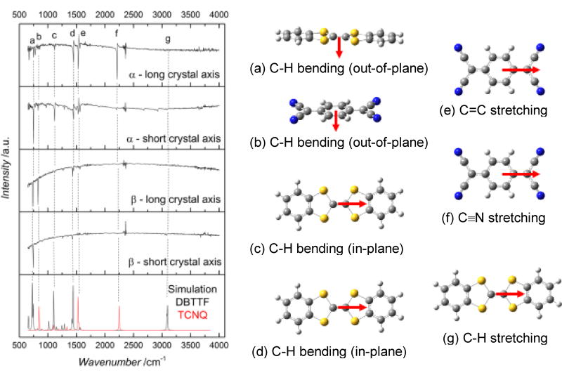
Polarized IR spectroscopy was applied to each crystal, and the results are shown in Figure 4. The anisotropies of the spectra shown in this figure point to another key difference between the two polymorphs. For the α-polymorph, the observation of the vibrations labelled c, d, e, and f, which are each parallel to the long axes of the molecular DBTTF and TCNQ, indicates that these axes are oriented parallel to the surface of the crystal. The out-of-plane C-H stretching of the DBTTF molecule (vibration a), which is perpendicular to the molecular plane, shows strong anisotropy and is most pronounced when the light is polarized along the long axis of the bulk crystal surface. Vibrations e and f, C = C and C ≡ N stretching on the TCNQ molecule respectively, occur in plane and have a transition moment parallel to the molecular long axis. They are strongest when the light is polarized parallel to the short axis of the bulk crystal. Together, a, e, and f show that the molecular CT stack axis is parallel to the long axis of the crystal, in agreement with the absorption data. The β-polymorph, on the other hand, shows strong anisotropy in the vibration labelled “b”, and weak intensity in all directions for vibrations c, d, e, f, and g. This indicates that the short molecular axis of the DBTTF and TCNQ is parallel to the bulk crystal surface, and the stack axis is parallel to the short axis of the crystal, confirming our optical absorbance measurements.
Figure 4.
IR spectra for each type of crystal, polarized along both the long and short axes. Vibrations a-g are identified within the spectra, and pictured at the right. CN stretching (f) frequency shifts with respect to TCNQ charge.
A summary of D and A molecular orientation within the single crystals of each polymorphs, as well as with respect to the crystal edge parallel to the substrate, as obtained by combining the above mentioned measurements is included in Figure 5.
Figure 5.
Molecular orientation of DBTTF and TCNQ, respectively with respect to the crystal surface, and long and short bulk crystal axes. The xy plane is drawn as a guide, and is oriented to the crystal face. The α-polymorph crystal structure is used here, while the β-polymorph structure is approximated based on spectroscopy.
2.3. Degree of Charge Transfer
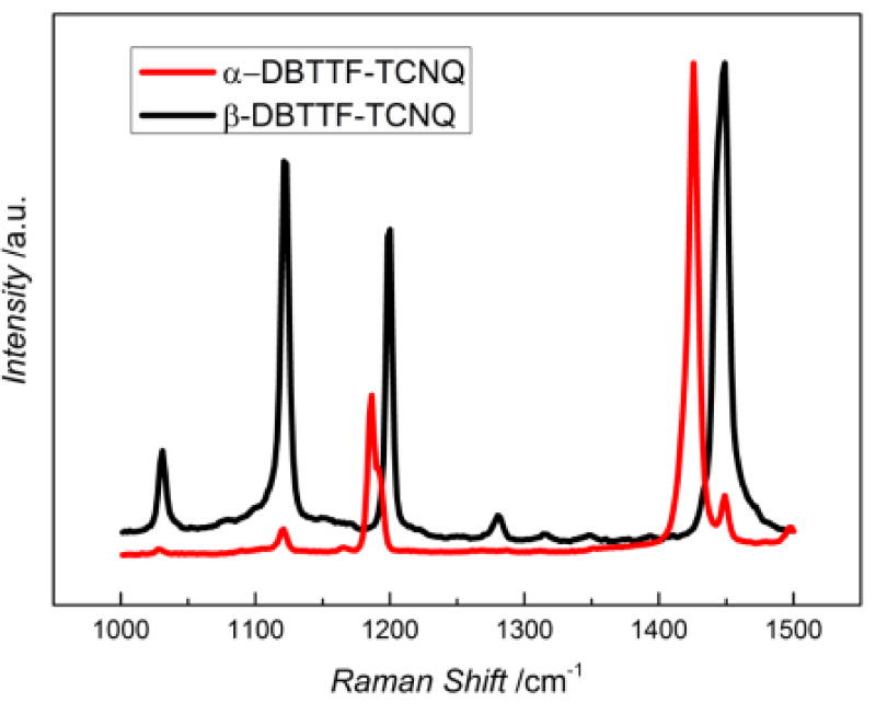
Charge-transfer complexes are characterized by partial ionicity. Organic metals fall in the 0.5e – 0.75e range, although having such degree of charge transfer does not guarantee metallicity[2]. Techniques to quantify the degree of charge transfer exploit the change in the bond lengths and vibration frequencies of the acceptor/donor as a result of the partial addition/loss of charge. These include Raman and IR spectroscopies, X-ray and neutron scattering[18,19,25,35–37]. In this study we determined the degree of charge-transfer via Raman spectroscopy by evaluating the dependence of the TCNQ ν4 (exocyclic C=C stretching) vibration frequency on the surrounding charge[36]. The results are shown in Figure 6. In a neutral molecule, this mode appears at 1454 cm−1, while in the completely ionized case it occurs at 1395 cm−1[36]. The α-polymorph exhibited a shift to 1426 cm−1 in our measurements, corresponding to a degree of charge transfer of 0.5e. This value is in agreement with the value reported in the literature based on IR spectroscopy[25]. The weakly intense peak present at 1450 cm−1 was predicted to correspond with the C=C stretching on the donor moiety, and was thus not used for the calculation of the degree of charge-transfer. The β-polymorph appears more neutral, showing a very modest shift to 1448 cm−1, which corresponds to ρ = 0.13e.
Figure 6.
The Raman spectrum for each polymorph from 1000 to 1500 cm−1. The ν4 C=C stretching for neutral TCNQ occurs at 1454 cm−1 and for the TCNQ anion at 1395 cm−1, and is assumed to shift linearly based on acquired charge. The spectrum obtained for the α-DBTTF-TCNQ is shown in red and for the β-DBTTF-TCNQ in black.
XPS provides a complementary measurement to detect elements in different electronic states, but it only probes the first 5–10 nm of the crystal surface. As shown in Figure 3a, the spectral shapes of the DBTTF in the α- and β-structures have pronounced differences. The S atoms in the α-polymorph display a shoulder from 165–166 eV and show higher intensity at 164.5 eV when compared to the β-DBTTF-TCNQ polymorph. The spectra were deconvoluted and we applied the methods used by Medjanik, et al[38] for spectral assignment. The states of the sulfur atoms here are adequately described by two pairs of lineshapes, which suggests that the atoms detected at the surface of the α-polymorph are in two different chemical (or electronic) environments – one charge-transfer state and one neutral. In contrast, the S 2p spectrum of the β-DBTTF-TCNQ shows that the S atoms are in one chemical (or electronic) state. The single state present in the β-DBTTF-TCNQ spectrum is assigned to neutral DBTTF and this indicates that the degree of CT at the surface of the crystal is zero. The fraction of charged DBTTF molecules in the α-polymorph based on the fitted results of the S 2p spectrum is 0.31 ± 0.02. While we cannot confidently report ρ based on this measurement, it is clear that the α-polymorph contains more charged S atoms than the β-polymorph. The N1s spectra for the polymorphs also convey the differences between the two types of crystal, and are shown in Figure 3b. The α-polymorph is described by three lineshapes: one centered at 398.6 eV, one centered at 399.6 eV, and one centered at 402.0 eV. Similar to the studies focusing on TTF-TCNQ[39] and F4-TCNQ[40], we assign the low-binding-energy feature at 398.6 eV as the TCNQ moiety within the CT complex that does undergo CT and the high-binding-energy feature at 399.6 eV as the TCNQ moiety that does not undergo CT. The N 1s spectrum of the β-DBTTF-TCNQ displays a prominent peak at 399.2 eV, and a less intense, broad peak at 401.8 eV. This spectrum is very similar to earlier reports of TCNQ[41], and we assign the main peak as the direct N 1s photoemission of electrons in the TCNQ moiety of the CT crystal while the broad feature is assigned as a shake-up satellite feature. The fraction of charged TCNQ in the same polymorph is estimated from the fit results in Figure 2b as (0.23 ± 0.02). The fraction of DBTTF molecules that undergo CT is greater than TCNQ within the α-DBTTF-TCNQ polymorph. This provides structural insight into the localization of the charge within the α-DBTTF-TCNQ polymorph, where a greater amount of charge is near the thiophene group relative to the cyano group. The XPS results also provide additional evidence of the different electronic structures between the two polymorphs, where CT is detected at the surface in the α-DBTTF-TCNQ structure and not in the β-DBTTF-TCNQ.
The complementary measurements described in this section confirm that the α-polymorph exhibits a high degree of charge transfer of 0.5e, while the β-polymorph is nearly neutral. Such a difference results from the shift in the molecular overlap of the donor and acceptor molecules, in agreement with the theoretical work suggesting that ρ, similar to charge carrier mobility, depends on the molecular overlap[23].
2.4. Charge Transport in DBTTF-TCNQ Polymorphs
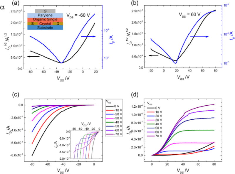
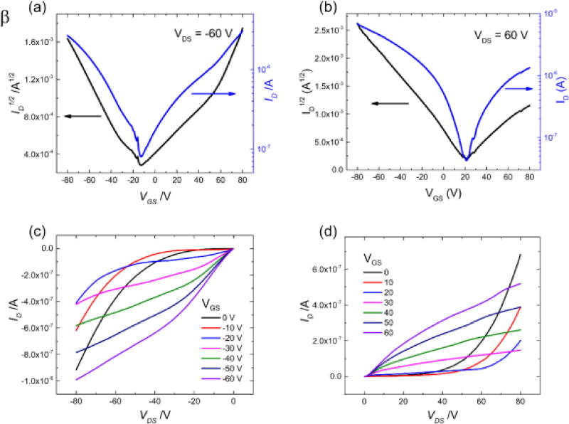
In this section we present the effect of the differences in the crystal structure and partial ionicity on the charge transport in this material system. We measured the electrical characteristics of the two DBTTF-TCNQ polymorphs by fabricating single crystal OFETs of the top-gate, bottom-contact design. The device structure is included as an inset in Figure 7a. At least 30 crystals of each polymorph were investigated and all measurements were performed along the D/A stack direction. Current-voltage (I-V) characteristics for a typical α-polymorph device are shown in Figure 7, while in Figure 8 we include the I-V curves for the β-polymorph. Transfer characteristics were taken for VDS = ±60 V, and the hole and electron mobilities, μh and μe, were calculated from the saturation regime using standard procedures[42–44]. The non-linear behavior of the low VDS region of the output characteristics originates from the injection barriers between the metal contacts and the semiconductor materials, which are inherent in ambipolar FET devices.
Figure 7.
Electrical characteristics for the α-polymorph, with device structure shown as an inset of plot (a). The channel geometry is L/W = 0.85. The transfer characteristics for negative drain voltage are shown in (a) and for positive drain voltage in (b), with the black axis showing the square root of the drain current versus the voltage and the blue axis showing a log-scale plot of the drain current versus voltage. The output characteristics for the α-polymorph are shown for negative and positive gate voltage are shown in (c) and (d) respectively, indicating electron-favored transport. The inset in plot (c) shows the output characteristics scaled to lower current values to show the hole accumulation, which is about one order of magnitude smaller than the ambipolar current demonstrated when |VGS-VT| < |VD|.
Figure 8.
Electrical characteristics for the β-polymorph. The channel geometry is L/W = 0.75. The transfer characteristics for negative drain voltage are shown in (a) and for positive drain voltage in (b). Panels (c) and (d) show the output characteristics for the β-polymorph.
Ambipolar transport is observed in both polymorphs, but the differences between hole and electron enhancement are clear. In the α-polymorph the electron transport is dominant, with the average electron mobility μeα = 0.4 ± 0.2 cm2V−1s−1 being one order of magnitude greater than the average hole mobility in the same crystals, μhα = 0.04 ± 0.02 cm2V−1s−1. Differences in measured mobility values for these single crystals are the result of small variations in the orientation of the crystal with respect to the source and drain contacts, as well as different crystal quality. Nevertheless, the electron mobility is always larger than the hole mobility, with a ratio of 10–12 between the two being typical. These results are in agreement with those reported previously for solution grown microrods of the α-polymorph DBTTF-TCNQ on similar contacts, though the electron mobility in our devices is slightly higher[33]. This is likely due to the fact that we used parylene dielectric instead of bare SiO2; numerous semiconductor materials have been shown to exhibit diminished electron transport on SiO2 dielectric compared to a polymer or self-assembled monolayer-treated SiO2 dielectric because of the increased density of trapping states formed here[45,46]. We note, however, that another study showed only electron transport in the α-polymorph, with a similar device structure, but at much lower applied voltages (linear regime of device operation)[47]. We believe hole transport is observed in our studies because the devices are biased at higher drain voltages. The β-polymorph shows contrary behavior and favors hole transport with mobilities of μhβ = 0.1 ± 0.07 cm2V−1s−1 and μeβ = 0.03 ± 0.02 cm2V−1s−1, as shown in Figure 8. For all measured samples, a ratio of 3–5 between the two values is typical, with the hole mobility always surpassing the electron mobility. These trends are consistent for all the crystals we investigated in this study.
3. Discussion
It is well known that the differences in crystal structure that are inherent in polymorphs result in modifications in the band structures and physical properties[48,49]. This has been measured, for example, in thin films of diindenoperylene by a combination of UPS, IPES (inverted photoemission spectroscopy), low-energy electron diffraction (LEED), and XPS[50]. In order to understand the differences induced in the band structure of the DBTTF-TCNQ polymorphs, we performed both UV-Vis-NIR absorption spectroscopy and UPS measurements. Details about these measurements and their results are included in the supplementary information (Figure S3). The optical absorption measurements show that the α-polymorph CT band peaks at 0.78 eV, while the β-polymorph peaks at 0.73 eV. Each of these absorption bands results from the CT excitations from the HOMO level of the DBTTF to the LUMO level of TCNQ and thus provide an estimate for the band-gap of each DBTTF-TCNQ polymorph, suggesting a narrower value for the β-polymorph. These results demonstrate that (1) polymorphism in molecular crystals results in changes in HOMO/LUMO levels which may impact charge injection, and (2) the band-gap formation of the CT salt is more complex than simply mixing the levels of the donor and acceptor species. Based on the UPS results, we find a HOMO shift with respect to the Fermi energy level of 1.03 ± 0.07 eV for the α-polymorph and 1.10 ±0.05 eV for the β-polymorph, which implies that the different polymorphs have different hole-injection barriers when contacted to Au source/drain electrodes. While we cannot unambiguously quantify the difference in HOMO between the two structures because the standard deviations in these measurements are of similar magnitude to the energy shift value (ΔEHOMO=0.07eV), the UPS measurements suggest that the shift is present. Such a small shift, however, is not sufficient to explain the differences observed in charge transport, as it can be overcome by band bending.
The existence of distinct unit cells implies that the molecular overlap between the donor (DBTTF) and the acceptor (TCNQ) is different between the two polymorphs (see Figure 5). Calculations and experimental work previously performed on mono-molecular crystals showed that very small changes in the intermolecular overlap of the adjacent organic semiconductor molecules can yield dramatic changes in intermolecular electronic coupling, which directly impact charge transport properties[51–53]. In order to evaluate this effect in CT complexes, in parallel to our experimental measurements aimed at understanding the electronic structure of the polymorphs, we performed DFT calculations on the derived β-structure and compared the results with those previously reported on the α-polymorph. For the β-polymorph, the effective electron coupling values for holes and electrons along the stacking directions are estimated to 8 meV and 18 meV, respectively. In addition to the electronic interaction along the stacking directions, significant direct electronic coupling was estimated between neighboring donor molecules (th =14 meV) and between neighboring acceptor molecules (te = 11 meV). Overall, the electronic interaction for holes and electrons is comparable. Thus, the band structure calculations (see Figure S4) indicate that the conduction band and valence band widths are nearly equal (150 meV and 138 meV, respectively). The calculated electronic couplings result in an effective mass for holes of 0.94 m0 (the effective mass calculations for electrons have not converged), where m0 represents the electron mass in vacuum. The couplings derived for the β-polymorph are much smaller compared to the reported values for the α-polymorph, where the effective electronic couplings along stacking directions for holes and electrons were estimated as 85 meV and 71 meV, respectively[5]. As result, the effective masses for holes and electrons for the α-polymorph were found to be about two times smaller than the value estimated here for holes in the β-polymorph. To conclude, the electronic structure results suggest a more efficient charge transport in the α-polymorph, in agreement with our experimental results. In addition, they also point to an intrinsic balanced transport in both polymorphs, i.e. similar mobilities for electrons and holes in each type of crystal. In devices, however, the presence of extrinsic factors such as the injection barriers formed at the metal/semiconductor interface or polarization at the semiconductor/dielectric interface may, and indeed have, led to different results. Takahashi, et al, showed that in OFETs fabricated on the α-polymorph,[7,47] electron-only transport, ambipolar transport, and hole-only transport can be achieved by selecting source-drain electrodes of different work functions. Since we used the same type of metal (gold) to contact both polymorphs in the present study, contact choice alone did not cause the differences we observed. A possible reason for the unbalanced electrical properties of the two crystalline structures may be related to their different responses to the presence of the trap states and defects, as we have demonstrated for another system[48]. A more significant contribution to these differences was suggested by a recent theoretical study, which showed that the effect of molecular overlap on electronic coupling in CTs is not necessarily mirrored for holes and electrons – i.e, their transfer integrals and therefore their mobilities, do not increase and decrease simultaneously[6]. Consequently, the bulk material may exhibit primarily hole, primarily electron, or ambipolar transport, depending on the strength of interactions of molecular orbitals participating in charge transport. For example, if the electronic coupling is dominated by the interaction between the donor HOMO and the acceptor LUMO, balanced electron/hole transport is expected. Otherwise, electron or hole dominant transport, or even unipolar transport may be achieved. In addition, the shifts in molecular overlap induce modulation of ρ, as proposed by Sini, et al[23], and confirmed here experimentally. The higher degree of charge transfer observed in the α-DBTTF-TCNQ suggests a higher crystal binding energy in the α-polymorph than the β-polymorph, as these two features are directly related[54]. Therefore, we attribute the differences in transport – electron-favored transport in the α-polymorph and hole-favored transport in the β-polymorph – to different D/A electronic coupling and the presence of different degrees of charge transfer between the D and A species, both caused by differences in the D/A overlap.
4. Conclusions
In conclusion, we discovered a new polymorph of the charge transfer complex DBTTF-TCNQ, which we refer to as the β-polymorph. The existence of two distinct crystalline structures with the same D/A ratio provides us with a unique system for the study of the impact of the donor-acceptor interactions on the optoelectronic properties of organic charge-transfer complexes. We find that the α-polymorph shows a large degree of charge transfer between the constituent molecules of about 0.5e, while in the β-polymorph the charge transfer is weak, quantified by a degree of charge transfer of about 0.1e. Interestingly, while both crystals exhibit ambipolar transport, electron-transport dominates in the α-polymorph, whereas hole-dominant charge transport is observed in the β-polymorph. The changes in the position of the HOMO/LUMO levels as a result of different crystalline structures are minimal as determined by UPS. We conclude that the differences detected in the electrical properties are a result of the interplay between the effect of the varying degree of charge transfer and electronic coupling between the donor and acceptor. These differences likely result in a variance in the molecular orbitals contributing to transport due to differing band structures between the two polymorphs.
5. Experimental Section
Selected Area Electron Diffraction (SAED)
SAED experiments were performed in a Zeiss Libra 120 transmission electron microscope at 120kV using a LaB6 filament and low electron dose conditions. Al (111) of 0.234 nm d spacing was used as the electron diffraction calibration standard.
X-ray Photoelectron Spectroscopy (XPS)
XPS measurements were performed in a commercial instrument (base pressure 1 × 10⁻⁹ Torr or better) equipped with a hemispherical electron energy analyzer and monochromatized Al Kα photons (1486.6 eV)[55]. Crystals of both polymorphs were laminated onto gold substrates and contacted to the substrate using silver epoxy.
IR Spectroscopy
IR spectra were measured by using a Thermofisher Scientific continuum IR microscope equipped with an iS50R FT-IR spectrometer. The anisotropy of the spectra were measured by polarizing the incident light with a wire-grid polarizer. For the spectral assignment, key vibrations were simulated by using GAUSSIAN09 with the 6-31G(d) basis set at the B3LYP level.
Raman Spectroscopy
The measurements were performed using a Renishaw inVia Raman microscope with a 532 nm excitation laser polarized along different crystal axes. As with the IR spectroscopy, spectral assignment was accomplished by simulating key vibrations using GAUSSIAN09 with the 6-31G(d) basis set at the B3LYP level.
Electrical Measurements
To fabricate the field-effect transistors, source/drain electrodes (5 nm Ti/45 nm Au) were patterned by photolithography and deposited by e-beam evaporation on a 200 nm SiO2 substrate that served the role of an insulating substrate. Following cleaning with hot acetone, hot isopropanol, and a UV/ozone treatment, the crystals were laminated by hand onto the substrate as they were thin enough to stick by electrostatic adhesion. The crystals were aligned with the contacts so that the charge-transfer stack axis was directed across the OFET channel. To achieve the top-gate configuration, 300–750 nm N-parylene (εr = 2.65, thickness determined from capacitance measurements) was deposited onto the crystals following a procedure described elsewhere[56,57], and silver (60 nm) was thermally evaporated to act as a gate contact. Electrical properties were measured in air and in the dark by using an Agilent 4155C semiconductor parameter analyzer.
Electronic Structure Calculations
Following our recent work[58], the geometry optimization of the β-polymorph was performed by means of the αPBE functional with 30% nonlocal Hartree-Fock exchange contribution and using the 6-31G basis set. The calculations were performed using a 6 × 8 × 6 Monkhorst-Pack k-point mesh with a semi-empirical dispersion correction. This correction is based on the Grimme’s D2 model[59], but uses standard van der Waals radii as reported by Bondi[60] with the exception of hydrogen[61]. For the sake of comparison with the reported results for the α-polymorph[5], the electronic structure of the β-polymorph was computed at the B3LYP/6-31G level of theory using a 8 × 8 × 10 Monkhorst-Pack k-point mesh. All periodic boundary condition calculations were performed using the CRYSTAL14 program[62]. The electronic couplings between the frontier orbitals of the donor and of the acceptor (tH(D)-L(A)),,the effective couplings (theff, teeff) along the stacking direction and the electronic couplings between neighboring donor and acceptor molecules were evaluated at the B3LYP/6-31G level with the GAUSSIAN09 package[63].
Supplementary Material
Acknowledgments
We acknowledge Dr. Rachel Williamson of the Australian Synchrotron in her efforts to discern the structure for the β-DBTTF-TCNQ. We would also like to thank Dr. Alejandro Briseno and Dr. Marcos Reyes-Martinez at the University of Massachusetts at Amherst for their advice and training in preparing the parylene deposition system. This research was partially supported by the National Science Foundation under grants DMR-1105147 and ECCS-1254757 and by the U.S. Army Research Laboratory and U.S. Army Research Office under contract/grant number W911NF-13-1-0387. KPG acknowledges the NSF Graduate Research Fellowship Program (GRFP) and Graduate Research Opportunities Worldwide (GROW) under grant DGE-0907738. TEM (J.C.) experiments were conducted at the Center for Nanophase Materials Sciences, which is a DOE Office of Science User Facility.
Footnotes
Supporting Information is available from the Wiley Online Library or from the author.
Contributor Information
Dr. Katelyn P. Goetz, Department of Physics, Wake Forest University, Winston Salem, NC 27109, USA
Dr. Jun’ya Tsutsumi, Flexible Electronics Research Center, National Institute of Advanced Industrial Science and Technology (AIST), Tsukuba, Ibaraki 305-8562, Japan
Dr. Sujitra Pookpanratana, Engineering Physics Division, National Institute of Standards and Technology (NIST), Gaithersburg, Maryland 20899-1070, USA
Dr. Jihua Chen, Center for Nanophase Materials Sciences, Oak Ridge National Laboratory, Oak Ridge, TN 38831, USA
Nathan S. Corbin, School of Chemistry and Biochemistry and Center for Organic Photonics and Electronics Georgia Institute of Technology, Atlanta, Georgia 30332, USA
Dr. Rakesh K. Behera, School of Chemistry and Biochemistry and Center for Organic Photonics and Electronics Georgia Institute of Technology, Atlanta, Georgia 30332, USA
Dr. Veaceslav Coropceanu, School of Chemistry and Biochemistry and Center for Organic Photonics and Electronics Georgia Institute of Technology, Atlanta, Georgia 30332, USA
Dr. Curt A. Richter, Engineering Physics Division, National Institute of Standards and Technology (NIST), Gaithersburg, Maryland 20899-1070, USA
Dr. Christina A. Hacker, Engineering Physics Division, National Institute of Standards and Technology (NIST), Gaithersburg, Maryland 20899-1070, USA
Prof. Tatsuo Hasegawa, Flexible Electronics Research Center, National Institute of Advanced Industrial Science and Technology (AIST), Tsukuba, Ibaraki 305-8562, Japan Department of Applied Physics, The University of Tokyo, 7-3-1 Hongo, Bunkyo-ku, Tokyo 113-8656, Japan.
Prof. Oana D. Jurchescu, Department of Physics, Wake Forest University, Winston Salem, NC 27109, USA
References
- 1.Horiuchi S, Hasegawa T, Tokura Y. J. Phys. Soc. Japan. 2006;75:051016. [Google Scholar]
- 2.Goetz KP, Vermeulen D, Payne ME, Kloc C, McNeil LE, Jurchescu OD. J. Mater. Chem. C. 2014;2:3065. [Google Scholar]
- 3.Black HT, Perepichka DF. Angew. Chemie. 2014;53:2138. doi: 10.1002/anie.201310902. [DOI] [PubMed] [Google Scholar]
- 4.Black HT, Lin H, Bélanger-Gariépy F, Perepichka DF. Faraday Discuss. 2014:1. doi: 10.1039/c4fd00133h. [DOI] [PubMed] [Google Scholar]
- 5.Zhu L, Yi Y, Li Y, Kim EG, Coropceanu V, Brédas J-L. J. Am. Chem. Soc. 2012;134:2340. doi: 10.1021/ja210284s. [DOI] [PubMed] [Google Scholar]
- 6.Geng H, Zheng X, Shuai Z, Zhu L, Yi Y. Adv. Mater. 2015;27:1443. doi: 10.1002/adma.201404412. [DOI] [PubMed] [Google Scholar]
- 7.Takahashi Y, Hasegawa T, Abe Y, Tokura Y, Saito G. Appl. Phys. Lett. 2006;88:073504. [Google Scholar]
- 8.Tsutsumi J, Matsuoka S, Inoue S, Minemawari H, Yamada T, Hasegawa T. J. Mater. Chem. C. 2015;3:1976. [Google Scholar]
- 9.Park SK, Varghese S, Kim JH, Yoon S-J, Kwon OK, An BK, Gierschner J, Park SY. J. Am. Chem. Soc. 2013;135:4757. doi: 10.1021/ja312197b. [DOI] [PubMed] [Google Scholar]
- 10.Tayi AS, Shveyd AK, Sue AC-H, Szarko JM, Rolczynski BS, Cao D, Kennedy TJ, Sarjeant AA, Stern CL, Paxton WF, Wu W, Dey SK, Fahrenbach AC, Guest JR, Mohseni H, Chen LX, Wang KL, Stoddart JF, Stupp SI. Nature. 2012;488:485. doi: 10.1038/nature11395. [DOI] [PubMed] [Google Scholar]
- 11.Horiuchi S, Hasegawa T, Tokura Y. Mol. Cryst. Liq. Cryst. 2006;455:295. [Google Scholar]
- 12.Kagawa F, Horiuchi S, Tokunaga M, Fujioka J, Tokura Y. Nat. Phys. 2010;6:169. [Google Scholar]
- 13.Alves H, Molinari A, Xie H, Morpurgo AF. Nat. Mater. 2008;7:574. doi: 10.1038/nmat2205. [DOI] [PubMed] [Google Scholar]
- 14.Zhang J, Geng H, Virk TS, Zhao Y, Tan J, Di C, Xu W, Singh K, Hu W, Shuai Z, Liu Y, Zhu D. Adv. Mater. 2012;24:2603. doi: 10.1002/adma.201200578. [DOI] [PubMed] [Google Scholar]
- 15.Qin Y, Zhang J, Zheng X, Geng H, Zhao G, Xu W, Hu W, Shuai Z, Zhu D. Adv. Mater. 2014;26:4093. doi: 10.1002/adma.201400056. [DOI] [PubMed] [Google Scholar]
- 16.Pfattner R, Rovira C, Mas-Torrent M. Phys. Chem. Chem. Phys. 2015;17:26545. doi: 10.1039/c4cp03492a. [DOI] [PubMed] [Google Scholar]
- 17.Mori T, Inokuchi H. Solid State Commun. 1986;59:355. [Google Scholar]
- 18.Flandrois S, Chasseau D. Acta Crystallogr. Sect. B. 1977;33:2744. [Google Scholar]
- 19.Umland TC, Allie S, Kuhlmann T, Coppens P. J. Phys. Chem. 1988;92:6456. [Google Scholar]
- 20.Yamamoto HM, Hagiwara M, Kato R. Synth. Met. 2003;134–449:133. [Google Scholar]
- 21.Guionneau P, Kepert CJ, Bravic G, Chasseau D, Truter MR, Kurmoo M, Day P. Synth. Met. 1997;86:1973. [Google Scholar]
- 22.Mori T, Inokuchi H. Bull. Chem. Soc. Jpn. 1987;60:402. [Google Scholar]
- 23.Sini G, Sears JS, Brédas J-L. J. Chem. Theory Comput. 2011;7:602. doi: 10.1021/ct1005517. [DOI] [PubMed] [Google Scholar]
- 24.Zhu L, Yi Y, Fonari A, Corbin NS, Coropceanu V, Brédas J-L. J. Phys. Chem. C. 2014;118:14150. [Google Scholar]
- 25.Kistenmacher TJ, Emge TJ, Wiygul FM, Bryden WA, Chappell JS, Stokes JP, Chiang L-Y, Cowan DO. Solid State Commun. 1981;39:415. [Google Scholar]
- 26.Kobayashi H, Nakayama J. Bull. Chem. Soc. Jpn. 1981;54:2408. [Google Scholar]
- 27.Emge TJ, Wiygul FM, Chappell JS, Bloch AN, Ferraris JP, Cowan DO, Kistenmacher TJ. Mol. Cryst. Liq. Cryst. 1982;87:137. [Google Scholar]
- 28.Hunter CA, Sanders JKM. J. Am. Chem. Soc. 1990;112:5525. [Google Scholar]
- 29.Hu P, Ma L, Tan K, Jiang H, Wei F, Yu C, Goetz KP, Jurchescu OD, McNeil LE, Gurzadyan GG, Kloc C. Cryst. Growth Des. 2014;14:6376. [Google Scholar]
- 30.Buurma AJC, Jurchescu OD, Shokaryev I, Baas J, Meetsma A, de Wijs GA, de Groot RA, Palstra TTM. J. Phys. Chem. C. 2007;111:3486. [Google Scholar]
- 31.Tsutsumi J, Yamada T, Matsui H, Haas S, Hasegawa T. Phys. Rev. Lett. 2010;105:226601. doi: 10.1103/PhysRevLett.105.226601. [DOI] [PubMed] [Google Scholar]
- 32.Tsutsumi J, Matsui H, Yamada T, Kumai R, Hasegawa T. J. Phys. Chem. C. 2012;116:23957. [Google Scholar]
- 33.Wu H, Wang F, Xiao Y, Pan G. J. Mater. Chem. C. 2013;1:2286. [Google Scholar]
- 34.Vermeulen D, Zhu LY, Goetz KP, Hu P, Jiang H, Day CS, Jurchescu OD, Coropceanu V, Kloc C, McNeil LE. J. Phys. Chem. C. 2014;118:24688. [Google Scholar]
- 35.Herbstein FH. Crystalline Molecular Complexes: Structures and Principles; First. Oxford University Press; Oxford: 2005. [Google Scholar]
- 36.Matsuzaki S, Kuwata R, Toyoda K. Solid State Commun. 1980;33:403. [Google Scholar]
- 37.Chappell JS, Bloch AN, Bryden WA, Maxfield M, Poehler TO, Cowan DO. J. Am. Chem. Soc. 1981;103:2442. [Google Scholar]
- 38.Medjanik K, Gloskovskii a, Kutnyakhov D, Felser C, Chercka D, Baumgarten M, Müllen K, Schönhense G. J. Electron Spectros. Relat. Phenomena. 2012;185:77. [Google Scholar]
- 39.Rojas C, Caro J, Grioni M, Fraxedas J. Surf. Sci. 2001;485–546:482. [Google Scholar]
- 40.Koch N, Duhm S, Rabe JP, Vollmer A, Johnson RL. Phys. Rev. Lett. 2005;95:237601. doi: 10.1103/PhysRevLett.95.237601. [DOI] [PubMed] [Google Scholar]
- 41.Lindquist JM, Hemminger JC. J. Phys. Chem. 1988;92:1394. [Google Scholar]
- 42.Klauk H. Chem. Soc. Rev. 2010;39:2643. doi: 10.1039/b909902f. [DOI] [PubMed] [Google Scholar]
- 43.Kang MS, Frisbie CD. ChemPhysChem. 2013;14:1547. doi: 10.1002/cphc.201300014. [DOI] [PubMed] [Google Scholar]
- 44.Smits E, Anthopoulos T, Setayesh S, van Veenendaal E, Coehoorn R, Blom P, de Boer B, de Leeuw D. Phys. Rev. B. 2006;73:205316. [Google Scholar]
- 45.Chua L, Zaumseil J, Chang J, Ou EC-W, Ho PK-H, Sirringhaus H, Friend RH. Nature. 2005;434:194. doi: 10.1038/nature03376. [DOI] [PubMed] [Google Scholar]
- 46.He T, Stolte M, Burschka C, Hansen NH, Musiol T, Kälblein D, Pflaum J, Tao X, Brill J, Würthner F. Nat. Commun. 2015;6:5954. doi: 10.1038/ncomms6954. [DOI] [PubMed] [Google Scholar]
- 47.Takahashi Y, Hasegawa J, Abe Y, Tokura Y, Nishimura K, Saito G. Appl. Phys. Lett. 2005;86:063504. [Google Scholar]
- 48.Stevens LA, Goetz KP, Fonari A, Shu Y, Williamson RM, Brédas J-L, Coropceanu V, Jurchescu OD, Collis GE. Chem. Mater. 2015;27:112. [Google Scholar]
- 49.Troisi A, Orlandi G. J. Phys. Chem. B. 2005;109:1849. doi: 10.1021/jp0457489. [DOI] [PubMed] [Google Scholar]
- 50.Krause S, Schöll a, Umbach E. Org. Electron. 2013;14:584. [Google Scholar]
- 51.Kwon O, Coropceanu V, Gruhn NE, Durivage JC, Laquindanum JG, Katz HE, Cornil J, Brédas J-L. J. Chem. Phys. 2004;120:8186. doi: 10.1063/1.1689636. [DOI] [PubMed] [Google Scholar]
- 52.Brédas J-L, Calbert JP, da Silva Filho DA, Cornil J. Proc. Natl. Acad. Sci. 2002;99:5804. doi: 10.1073/pnas.092143399. [DOI] [PMC free article] [PubMed] [Google Scholar]
- 53.Coropceanu V, Cornil J, da Silva Filho DA, Olivier Y, Silbey R, Bredas J-L. Chem. Rev. 2007;107:926. doi: 10.1021/cr050140x. [DOI] [PubMed] [Google Scholar]
- 54.Torrance JB, Silverman BD. Phys. Rev. B. 1977;15:788. [Google Scholar]
- 55.The identification of commercial equipment or vendor is not intended to imply recommendation or endorsement by NIST, nor is it intended to imply that the materials or equipment identified are necessarily the best available for the purpose.
- 56.Podzorov V, Pudalov VM, Gershenson ME. Appl. Phys. Lett. 2003;82:1739. [Google Scholar]
- 57.Reyes-Martinez MA, Crosby AJ, Briseno AL. Nat. Commun. 2015;6:6948. doi: 10.1038/ncomms7948. [DOI] [PMC free article] [PubMed] [Google Scholar]
- 58.Fonari A, Corbin NS, Vermeulen D, Goetz KP, Jurchescu OD, McNeil LE, Bredas JL, Coropceanu V. J. Chem. Phys. 2015;143:224503. doi: 10.1063/1.4936965. [DOI] [PubMed] [Google Scholar]
- 59.Grimme S. J. Comput. Chem. 2006;27:1787. doi: 10.1002/jcc.20495. [DOI] [PubMed] [Google Scholar]
- 60.Bondi A. J. Phys. Chem. 1964;68:441. [Google Scholar]
- 61.Civalleri B, Zicovich-Wilson CM, Valenzano L, Ugliengo P. CrystEngComm. 2008;10:405. [Google Scholar]
- 62.Dovesi R, Orlando R, Erba A, Zicovich-Wilson CM, Civalleri B, Casassa S, Maschio L, Ferrabone M, De La Pierre M, D’Arco P, Noël Y, Causà M, Rérat M, Kirtman B. Int. J. Quantum Chem. 2014;114:1287. [Google Scholar]
- 63.Frisch MJ, Trucks GW, Schlegel HB, Scuseria GE, Robb MA, Cheeseman JR, Scalmani G, Barone V, Mennucci B, Petersson GA, Nakatsuji H, Caricato M, Li X, Hratchian HP, Izmaylov AF, Boino J, Zheng G, Sonnenberg JL, Hada M, Ehara M, Toyota K, Fukuda R, Hasegawa J, Ishida M, Nakajima T, Honda Y, Kitao O, Nakai H, Vreven T, Montgomery JE, Peralta JA, Jr, Ogliaro F, Bearpark M, Heyd JJ, Brothers E, Kudin KN, Staroverov R, Kobayashi VN, Normand K, Raghavachari J, Rendell A, Burant JC, Iyengar SS, Tomasi J, Cossi M, Rega N, Millam JM, Klene M, Knox JE, Cross JB, Bakken V, Adamo C, Jaramillo J, Gomperts R, Stratmann RE, Yazyev O, Austin AJ, Cammi R, Pomelli C, Ochterski JW, Martin RL, Morokuma K, Zakrzewski VG, Voth GA, Salvador P, Dannenberg S, Dapprich JJ, Daniels AD, Farkas Ö, Foresman JB, Ortiz JV, Cioslowski J, Fox DJ. Gaussian 09 Revision E.01. 2009 [Google Scholar]
Associated Data
This section collects any data citations, data availability statements, or supplementary materials included in this article.


