Abstract
High-density on-chip electrochemical biosensor arrays are advancing toward a crucial role in health monitoring and development of new medicines and medical treatments. Nanopore and ion channel based sensors especially have great potential but present demanding resolution/speed/power/area requirements on instrumentation circuits. This paper presents a pixel-level current readout circuit and new group-cluster architecture to address the circuit challenges in high performance biosensor arrays. Fabricated in 0.5 μm CMOS, this electrochemical voltammetry circuit achieves 7.2 pArms noise in an 11.5 kHz bandwidth and only consumes 21 μW power and 0.06 mm2 area per readout channel. Cyclic voltammetry experiments in a potassium ferricyanide solution and patch-clamp whole-cell experiments were performed to validate the circuit’s feasibility for electrochemical biosensor applications.
Index Terms: Current readout, compact, ultra-low power, electrochemical, sensor array
I. INTRODUCTION
Biosensors play crucial roles in health monitoring and biomedical research into new forms of treatment and drug discovery. For example, biosensors can diagnose and monitor diseases by detecting biomolecules (disease indicator) such as glucose, DNA and proteins [1-5]. Biosensors are also important for development of medicines for chronic pain, hypertension, cancer and epilepsy [6]. Electrochemical techniques are important for biosensor development because electrochemical sensors have unique features such as high sensitivity, selectivity, low power consumption, and suitability for miniaturization [7]. Electrochemical biosensors can detect many hazardous biological targets, including pathogens such as cholera toxin, mycotoxins, hepatitis, bacillus anthracis, rabies virus, and E. Coli [8-13].
Ion channel proteins are one class of biosensor interface that are especially important because of their unique role in biology and their great potential as drug targets [6]. Ion channels are typically studied within the lipid bilayer of a living cell, which has a very limited lifetime outside of its natural environment, generally less than 1 hour. In addition, formation of ion-channel-containing membranes in the laboratory has a very low yield, around 30% based on empirical evidence [14]. In contrast, traditional electrochemical studies take a significant amount of time to setup and perform, making it difficult to obtain the quantity of data needed to complete biomedical research. DNA sequencing using electrochemical techniques suffers from this experiment-time vs. information tradeoff as well. New solutions, such as a high-throughput artificial membrane protein array [15] and a nano-patch-clamp integrated system [16, 17] have been proposed to address these issues and permit rapid parallel measurement. These high-throughput on-chip biosensor arrays could also be adapted to antibody/antigen immunosensor development.
Complementary metal–oxide–semiconductor (CMOS) technology for integrated circuits enables the implementation of high performance, low power and low cost circuits within tiny silicon chips. Novel integration technologies enable electrochemical transducers to be integrated monolithically with CMOS circuits on a single chip to decrease system cost and size while reducing noise to improve detection limits [18]. Our group has introduced the lab-on-CMOS platform for high-throughput biosensor arrays as shown in Fig. 1 [15, 19]. Here, a sensor array is formed on the surface of a CMOS instrumentation chip for low-noise and high-density measurement, and a planar carrier package extends the surface area beyond CMOS chip to allow integration a with multi-channel microfluidic component that transports, mixes, etc. biological samples and control solutions. Highly integrated biosensor array platforms like this require a readout circuit with pico-ampere level noise, micro-watt power consumption, ultra-compact size and >10 kHz bandwidth to allow parallel measurement applications [6, 14].
Fig. 1.
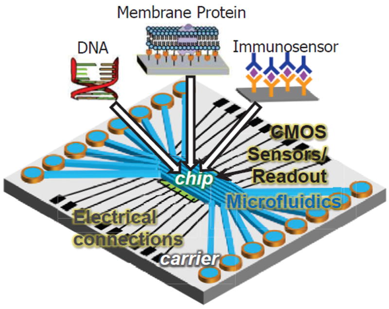
Concept structure a lab-on-CMOS platform of a high-throughput on-chip biosensor array. Over 100 sensing elements can be implemented on this platform.
The literature contains numerous examples of CMOS electrochemical current readout circuits for multi-channel measurement [20-23], including a recent review [18]. However, these circuits mainly target low-frequency/DC current measurement. Although CMOS instruments have been reported to measure DNA in nanopores and ion channel currents achieving pA-noise over 10 kHz bandwidth recording [16, 24, 25], these circuits consume a large amount of power or occupy large area and are not well suited for high-density on-chip biosensor array applications. In addition, a chopper-stabilized current conveyor circuit that achieves very low noise has been reported [26]. However, it has a very low current gain that requires a high precision analog-to-digital convertor (ADC), which consumes significant area and power.
This paper presents a new CMOS instrumentation circuit for electrochemical biosensor arrays with over 100-channels/chip. The circuit achieves pA level noise, micro-watt power consumption per channel, ultra-compact size and over 10 kHz bandwidth. This paper expands on preliminary results in [6] by more thoroughly describing the circuit design and noise analysis and by reporting new results of post-fabrication circuit characterization and electrochemical and biological experiments. Section II discusses instrumentation requirements and compares traditional current readout performance to identify starting points for this work. Section III presents the pixel-level current readout circuit and new group-cluster architecture that addresses key limitations of exiting designs. Section IV describes the circuit block design and implementation, and section V presents noise analysis to optimize circuit component sizes. Section VI reports the fabricated circuit’s performance along with electrochemical and biological experiment results.
II. INSTRUMENTATION REQUIREMENTS AND ANALYSIS OF CURRENT READOUT OPTIONS
A. Instrumentation Requirements
The critical performance factors in CMOS circuits for biosensor arrays include noise, input current range, bandwidth, power and area. Biosensor response current signal level and bandwidth vary significantly with the type of biomolecules employed. Table 1 lists reported characteristics for a sub-class of electrochemical biosensors featuring membrane protein or nanopore interfaces which exhibit a combination of resolution and bandwidth needs that are more demanding than most biosensor applications. This work aims to meet these needs while also providing a signal range suitable for most biosensor applications. Thus the readout circuit design requirements were set to a 10 nA bidirectional current range with noise down to 10 pA noise in a 10 kHz bandwidth. In addition to these signal requirements, this work targets applications with high throughput on-chip electrochemical biosensor arrays, which imposes stringent requirements on readout circuit area and power. For example, to implement over 100 channels in a 2.5 mm × 2.5 mm chip area, the circuit area per channel must be less than 0.0625 mm2. For on-chip biosensors, the chip can act as a heater and degrade or denature bio-interfaces A heat flux of 80 mW/cm2 can cause damage to biological tissue [27]. Thus, for an on-chip array with a circuit area per channel of 0.0625 mm2, the power consumption per channel must be less than 50 μW. Furthermore, because of the inherent tradeoff between a circuit’s performance and its area and/or power, the need to simultaneously address these stringent requirements makes readout circuit design even more challenging.
TABLE I.
CURRENT SPECIFICATIONS ON NOISE, BANDWIDTH AND CURRENT RANGE FOR ELECTROCHEMICAL BIOSENSOR STUDY
B. Analysis of Current Readout Topologies
To measure pA level currents, the electrochemical readout circuit must have both low noise and large amplification gain. The most common basis for an electrochemical current readout circuit is a transimpedance amplifier (TIA), which can be implemented as a resistive feedback configuration or a switched-capacitor feedback configuration [26, 28, 29]. However, both of these configurations have drawbacks for high-density biosensor array recording.
To measure pA currents, the resistive feedback TIA may use a large feedback resistor (>1 GΩ) to achieve high signal-to-noise ratio and high gain, which requires considerable chip area. Although an active feedback structure has been reported to reduce the feedback resistor area for pA level noise, the area was so large that only eight recording channels could be implemented in a 9 mm2 area [25, 30]. In addition, feedback resistance mismatch due to process variations generates large gain variation in a multi-channel readout, requiring additional cost for gain calibration.
The switched-capacitor feedback TIA behaves like an integrator and can measure small currents with large gain and pA noise by charging a small feedback capacitance over a long period of time. As a result, the switched-capacitor feedback TIA requires much less area than the resistive feedback TIA. However, a long integration time necessitates a low signal bandwidth, according to the Nyquist–Shannon sampling theorem. In addition, as a discrete-time solution, the switched capacitor TIA has switching noise and noise alias problems [31, 32] and shows larger noise than the resistive feedback approach at bandwidth over 2 kHz [31]. Furthermore, the switching noise in this circuit injects charge to the sensing electrode and disturbs the electrochemical charge balance at the electrode-electrolyte interface. As a result, low concentration redox reactions cannot be properly observed [26]. Also, as with the resistive TIA, feedback mismatch can add calibration cost.
In contrast to TIAs, the current conveyor topology is an attractive solution for high-density on-chip biosensor arrays because it can achieve very low power and very small area[20]. Current conveyors function like a current buffer, which isolates the electrochemical sensor from following stages. The current conveyor holds the sensing electrode voltage at a constant value and provides an output current that is linearly proportional to the input current. Current conveyors can be as simple as an operational transconductance amplifier (OTA) and one additional transistor, and they do not need large capacitors or resistors [33], making them compact with power consumption down in the micro watt level. In addition, as a continuous time solution, the current conveyor does not inject charge into the electrode-electrolyte interface or affect redox reactions. These features make the current conveyor an attractive solution for high-density on-chip electrochemical biosensor array.
Some current conveyor topologies have been built for electrochemical sensing, but all exhibit limitations for the target applications. The bandwidth of the circuit in [33] is less than 1Hz. The circuit in [34] shows large noise and needs a high-resolution current-to-digital convertor, which occupies a large area and requires additional power. The design in [26] requires additional chopper clocks that take more area and power, and has very low current gain that requires a high-resolution current-to-digital convertor occupying extra area and power.
A qualitative performance comparison between the two TIAs and a current conveyor is summarized in Table II. Although each option has some strengths and weaknesses, the current conveyor has unique advantages for the target application and was chosen as the basis for the new topology introduced below.
TABLE II.
PERFOMRANCE COMPARISON OF TRADITIONAL CURRENT READOUTS FOR TARGET APPLICATIONS
| Circuit | Pros | Cons |
|---|---|---|
|
| ||
| Res. feedback TIA | Simple; Bidirectional; No interference to redox reactions | Large area, Large gain variation |
|
| ||
| Switched- cap. TIA | Bidirectional; Medium area; Low noise | Switching noise and noise folding; Large gain variation; Interference to redox reactions. |
|
| ||
| Current conveyor | Very small area; Low power; No interference to redox reactions; | Large noise |
| Low gain | ||
III. INSTRUMENTATION ARCHITECTURE DESIGN
A current conveyor topology and a new system architecture was developed to overcome the disadvantages of traditional current conveyors while maintaining the area and power efficiency desired for high-throughput on-chip electrochemical biosensor arrays. The current conveyor design provides accurate gain, good noise performance and sufficient bandwidth with a small transistor count. The proposed group-cluster system architecture provides large current gain with low area and power demands.
A. Current Conveyor Topology
The new, compact, current conveyor topology shown in Fig. 2 was designed to address the weaknesses in existing electrochemical current readout circuits. The desired input bias voltage, VWE, is set externally. The input sensor current, Iin, is taken from the working electrode (WE), and the voltage at WE is held to VWE by feedback in OTA1. The output current is defined as Io2. A high-precision current mirror was designed to achieve ultra-low current gain variation among different recording channels. With stage one providing a current gain of A and stage two a gain of B, the two-stage architecture in Fig. 2 achieves a large current gain of Io2/Iin = AB.
Fig. 2.
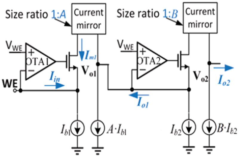
Simplified circuit block of a two-stage current conveyor for bidirectional current sensing with current gain of AB. WE is the current sensing electrode. Iin is the input current, Io1, and Io2 are the circuit output current of the two stages, respectively. Im, is the transistor current in the first stage.
The OTAs consume very low power because they are connected to transistor gates that do not require any drive current. As a continuous-time solution, this circuit does not inject charge to the electrode-electrolyte interface and thus does not affect redox reactions. Any voltage change at Vo1 or Vo2 can change the current mirror gain, thus Vo1 and Vo2 must be held at a DC voltage by their respective following stages. Compared to the single-stage current conveyor used in previous work [26, 33, 34], this two-stage topology can effectively boost the current gain. The higher gain allows the ADC to be implemented externally while maintaining good system noise performance, and external ADC placement helps to minimize the local heating of biosensor interfaces in on-chip systems like the Fig. 1 lab-on-CMOS platform.
B. Group-cluster Architecture
Sharing circuit resources in multi-channel recording instrumentation can effectively reduce the circuit area and power consumption. Fig. 3 (a) shows an example of a two-channel recording circuit utilizing the current readout in Fig. 2, where the “feedback” block in each stage of Fig. 3 represents all of the circuitry in the Fig. 2 OTA feedback path, i.e., the transistor, current sources, and current mirror. Because the OTA’s positive terminals are connected to the same voltage, VWE, a shared-segment OTA can be used [35]. As shown in Fig. 3 (b), the OTAs in each stage can be separated into two segments: a shared segment and unshared pixel segments. The shared segment is connected to a common bias voltage VWE and can be shared by all channels, leaving only a pixel segment needed for each channel.
Fig. 3.
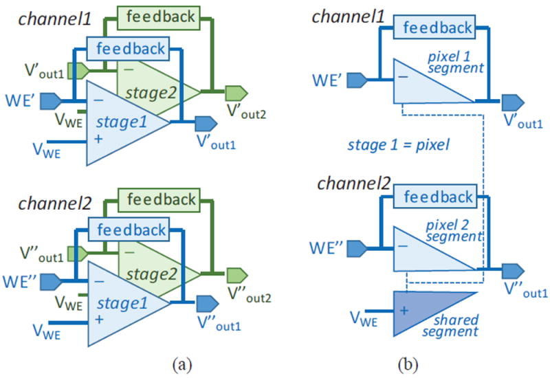
(a) Block diagram of two two-stage current readout channels with conventional OTAs, and (b) stage 1, pixel stage, with shared-segment OTAs. WE’ and WE’’ are the recording electrodes for channel 1 and 2, respectively.
To further reduce circuit area and power in a multi-channel recording system, a single second stage from Fig. 2, which we will now call a gain stage, can be shared by multiple pixel-stage channel amplifiers using a multiplexer in an interleaved architecture. By extending the shared segment concept to the gain stage amplifiers and combining the shared segment OTA concept and the interleaved two-stage structure, the resulting “group-cluster” architecture shown in Fig. 4 was introduced to achieve high performance with a large number of sensor channels. In Fig. 4, the first stage in Fig. 2 is represented by the pixel amplifier stage and can locally read sensor currents. The second stage in Fig. 2 is represented by the gain amplifier stage in Fig. 4 and provides additional current gain. Each recording channel has a pixel amp, and M pixels form a “cluster”. Each cluster is connected to one of N shared gain amps through an M:1 multiplexer, and N gain amps with their associated pixel clusters form a “group”. Thus each group supports M×N channels with M×N shared-segment pixel amps and N shared-segment gain amps. A full system can be composed of Q groups, where the gain amps of each group are connected through an N:1 multiplexer to Q-channel signal processing circuitry for filtering and digitization. Note that the high gain of the two-stage architecture relaxes the resolution requirement for digitization, allowing the ADC to be placed externally and reducing power consumption of an array readout chip. This power reduction combined with significant sharing of amplifier hardware resources for recording M×N×Q channels will minimize the local heating of biosensor interfaces in on-chip systems like the Fig. 1 lab-on-CMOS platform.
Fig. 4.
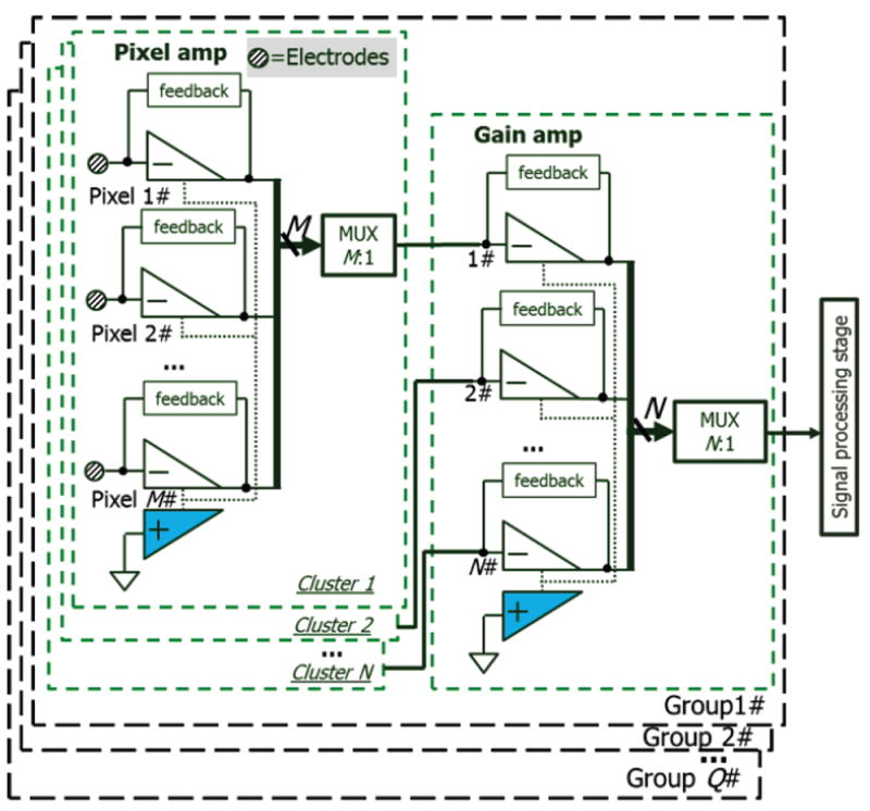
Block diagram of group-cluster architecture for M·N·Q recording channels. The highlighted blocks represent the shared OTA segments.
The maxim values of M, N and Q are limited by the desired channel sampling rate and the number of external ADCs employed. Assuming K ADCs with a conversion time of κ, the channel sampling rate can be expressed by K/(κ×M×N×Q). Moreover, a large M and N also reduces noise performance by affecting OTA common-mode rejection ratio, as discussed further in Section V.
IV. CIRCUIT BLOCK DESIGN AND IMPLEMENTATION
A. Current Conveyor Feedback Element
The input current range of the circuit depends directly on the magnitude of the current sources in Fig. 2, which is affected by current source mismatch. Defining ΔA as the deviation between current gain A and the true I11:I12 current ratio, and defining ΔB as the deviation between current gain B and the true I21:I22 current ratio, as shown in Fig. 5, we can write
| (1) |
Fig. 5.
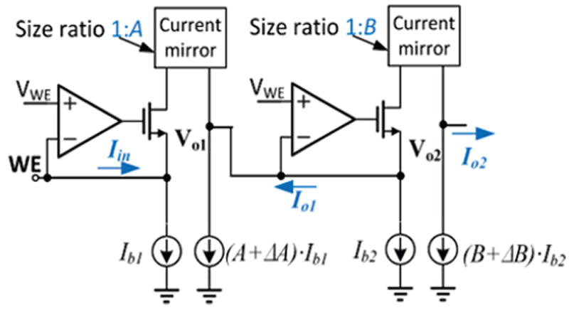
Analysis of current source mismatch effect on circuit performance.
The ΔA and ΔB deviations can generate a large output current offset and can reduce input current range. Thus, precision current mirrors and the current sources with well-matched transistor sizes are needed to enable small offset and large current range. With good matching techniques, 0.1% mismatch in transistor size can be achieved [36]. Assuming ΔA/A = 0.1%, and setting Ib1 =10nA, and Iin=10nA, equation. (1) estimates the Io1 offset error due to mismatch is only 0.5% of the input current.
To provide a precise current ratio, a cascoded current mirror structure was used. The schematic of the pixel amplifier is shown in Fig. 6. Mn(1,2,3) and MAn(1,2,3) form two current sources, equal to Ib and AIb, respectively. Transistors Mp(1,2,3) and MAp(1,2,3) form a cascoded current mirror to provide an accurate current ratio, A. Mp3,n3,Ap3,An3 are operated in deep linear region to reduce noise, and they function as degeneration resistances that are more compact than physical resistors in a CMOS process. A 1pF CL is used to improve circuit stability by creating a dominate pole at the gate of transistor Mf. Noise analysis and transistor size optimization are discussed in section V.
Fig. 6.
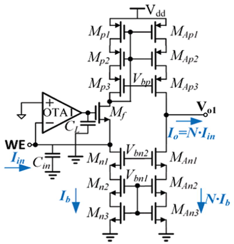
Schematic of a pixel amplifier. Cin is the total capacitance including parasitic capacitance and sensor capacitance. The transistors represents the “feedback” in Fig. 4.
B. Shared-segment OTA
A shared-segment OTA topology has been demonstrated to have desirable stability, bandwidth, and isolation between recording channels [35]. Because these performance advantages match our system requirements, this topology was used as a starting point to build the shared-segment OTA in Fig. 7, which serves as OTA1 in Fig. 6. Analysis of a structure that is similar to the OTA1 and Mf in Fig. 6 shows that the high open loop gain of OTA1 can largely suppress the noise contribution of transistor Mf [23]. Compared to the topology in [35], MpN3 and MnN3 in Fig. 7 were added to improve output impedance, which can help achieve large gain. Assuming the transconductance and output impedance of MpN3,nN3 are equal to gm,N3 and ro,N3, respectively, the output gain is improved by gm,N3×ro,N3. In the shared segment, the negative feedback loop formed by Mpb1, Mps1 and Mns3, regulates the common node voltage (Vc) for good isolation between pixel segments [35].
Fig. 7.
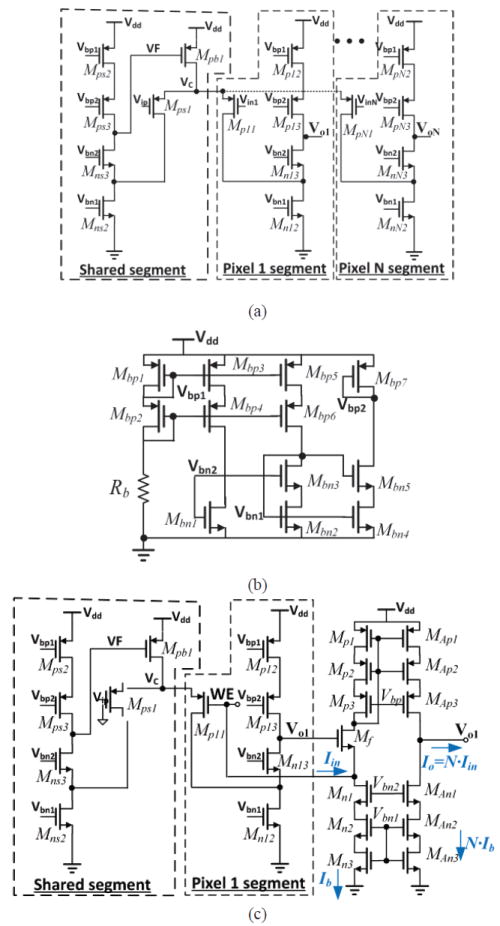
(a). Schematic of shared-segment structure OTA with N recording channels. (b) OTA bias circuit. (c). Full transistor-level diagram of a single-channel pixel amplifier stage.
The OTA bias circuit is shown in Fig. 7 (b), where resistor Rb and a current mirror were used to generate desired bias voltages. The complete transistor-level diagram of one channel of the pixel amplifier is shown in Fig. 7 (c). All the bias voltage are generated on chip. The OTA adds several mV offset to WE voltage. However, this error does not affect sensor performance because it is tolerated by most electrochemical experiments [37]. The power-supply-rejection ratio (PSRR) of the OTA is very high, especially at low frequency. Although Vdd ripple changes Vbn1, the impacts on Ib and AMb is turned into a common-mode signal by the current mirror Mp2 and Mp2’, and the resulting current is cancelled at node “Vo1” at low frequency. Simulation shows that the PSRR is 161dB in a 10 kHz bandwidth. The full OTA noise performance and design optimizations are discussed in section V.
C. Multiplexer
All of the multiplexers in Fig. 4 need to have low on-resistance for small voltage drop to maximize input current range. The multiplexers also need to provide DC bias to the outputs of inactive pixel/gain amplifiers to reduce settling time when any pixel/gain amplifier becomes active. Fig. 8 (a) shows the multiplexer topology that was implemented for two example recording channels with the multiplexer switch positions set to activate pixel amplifier #1. Single-pole double-throw switches were used to set the inactive pixel amplifier’s output at a DC bias that is equal to the middle of the power supply range. As a result, the turn-off resistance is very large and crosstalk noise is very small [38]. As shown in Fig. 8 (b), transmission gates with large W/L transistors were used as switches to reduce the turn-on resistance.
Fig. 8.

The schematic of (a) a M:1 MUX (multiplexer) in Fig. 4, and (b) the switches. Φ and Φ̄ are two inverted digital control signals.
D. Self-test Current Pulse Generator
To study the current through ion channel proteins, the biosensors would ideally be integrated directly on the surface of the CMOS readout chip to minimize the parasitic and connection capacitance and achieve good noise performance [25]. To generate simulated ion channel currents for circuit performance characterization and self-test functions, an on-chip test module was included. Ion channel currents are current pulses with pico-ampere amplitude Iamp and ≪ 1 ms pulse width Iwidth. A current splitter array can generate femtoampere current but cannot generate bidirectional current pulses [39]. To resolve this problem, a compact solution shown in Fig. 9 (a) was developed. A capacitor is connected to a pixel amplifier input, the voltage of which is VWE. Pulses of voltage Vin are applied on capacitor C to generate current pulses Iin, as shown in Fig. 9 (b). Assuming the slope of Vin during rising/falling times is SL, then Iamp = C×SL. An arbitrary signal generator was used to generate Vin.
Fig. 9.
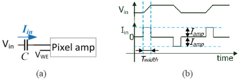
(a) The schematic and (b) waveforms of the current pulse generator.
E. Signal Processing Stage
The signal processing stage in Fig. 4 would digitize the gain amplifier output current and provide further digital signal processing and data storage. Because sensor current is greatly amplified before reaching to this stage, the ADC would not require ultra-low noise, greatly reducing its power and area in a CMOS implementation. To shorten the development time of the prototype current readout chip, a data acquisition card (NI USB-6259, National Instruments) was used to implement the digitization function. Since most ADCs take voltage inputs, a current-to-voltage (I/V) converter was included on the readout chip. A resistance feedback TIA was chosen for the I/V converter because it does not require any additional control signals. A feedback resistor array was implemented to allow testing of different current gains and ranges.
V. NOISE ANALYSIS
As the first stage, the pixel amplifier dominates circuit contributions to input referred noise. Noise analysis can assist in reducing noise by identifying major noise sources and optimizing component sizes. Transistors have two noise components: thermal noise and flicker noise. Transistors Mp3,n3,Ap3,An3 are operated in the linear region and act as resistors. To understand their impact on the noise of other transistors, we first ignore the flicker noise of Mp3,n3,Ap3,An3 and replace them with equivalent resistances Rp,n,Ap,An, as shown in Fig. 10 (a), to simplify the noise analysis. Next, we ran simulations to find the dimensions of Mp3,n3,Ap3,An3 for desired noise performance with that small flicker noise. The ratio of RAp and Rp was set to A to produce equal voltage drop on RAp and Rp. As a result, the source terminal voltages of Mp2 and MAp2 are equal. The same resistor ratio was also applied to RAn and Rn.
Fig. 10.
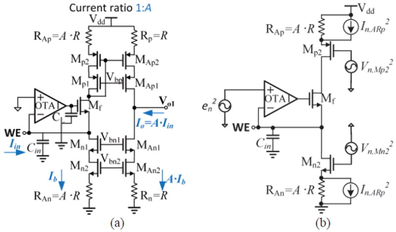
Equivalent circuit of pixel amplifier for noise analysis with (a) transistors in linear region replaced by resistors and (b) non-dominated noise source components removed to simply noise analysis.
Analysis of a similar structure for OTA1 and Mf has shown that the loop gain formed by OTA1 and Mf greatly reduces Mf’s contribution to the input referred current noise [23]. Transistors Mp1,n1,Ap1,An1 have negligible noise contribution as cascode transistors [40]. Ignoring these negligible noise sources, the input referred current noise of the pixel amplifier is
| (2) |
where f is the frequency, Cin is the total input capacitance including parasitic capacitance and ion-channel sensor capacitance, en is the input referred noise of OTA1, in,(x) represents the current noise of component x. Equation (2) shows that the noise currents of transistors Mn2,p2 and resistors RAn,Ap dominate the input referred noise. As a result, the Fig. 10 (a) can be simplified into Fig. 10 (b) for noise analysis by removing the non-significance current sources.
The OTA noise need to be minimized to reduce system noise. Large M or N (defined in Fig. 4) adds capacitance to node Vc in Fig. 7. This capacitance becomes a limiting impedance at high frequency and thereby reduces OTA common-mode rejection ratio (CMRR), which is equivalent to adding a common mode noise to en.
An expression relating the input referred current noise and transistor sizes enables noise performance optimization. Large transistor sizes are used to reduce flicker noise. The voltage noise of Mn2 can be expressed as [41]
| (3) |
where gm is the transconductance of Mn2, k is the Boltzmann constant, T is the operating temperature in Kelvin, and Kf is a constant for flicker noise calculation. Considering the degeneration resistor effect, Mn2’s current noise is
| (4) |
For a fixed Ib value, gm is equal to , where μn is the electron mobility, Cox is the gate oxide capacitance per unit area, Wn and Ln are the transistor Mn2 size. Mp2 noise contribution follows an equation similar to (4). Therefore, to reduce input referred current noise contribution of Mp2 and Mn2, the transistor area were set at very large area to reduce flicker noise. Large transistor length of Mp2 and Mn2 also helps provide accurate current gain by reducing transistor mismatch effects.
The current noise of resistance R is equal to 4kT/R. To reduce the resistor’s current noise contribution, the resistance should be large. Equation (4) shows that large Rn and Rp also reduce the noise contributions of Mn2 and Mp2’s. The sizes of transistors implementing Rn and Rp need to be large to reduce flicker noise. Based on this noise analysis, the chosen pixel amplifier transistor sizes are summarized in Table III. Based on noise simulations, the equivalent resistance of transistor M’n3 in Fig. 6 (shown as R in Fig. 10) was identified as 137 kΩ.
TABLE III.
TRANSISTOR SIZES OF PIXEL AMPLIFIER
| Transistor | W/L (μm/μm) | Transistor | W/L (μm/μm) |
|---|---|---|---|
| Mp2,p3 | 3/24 | MAn1 | 10*2.1/12 |
| Mp1 | 4.2/12 | MAn2,An3 | 10*1.5/48 |
| Mn1 | 2.1/12 | Mps1,p11 | 40*4.2/1.2 |
| Mn2,n3 | 1.5/48 | Mns2,n12 | 8.4/2.4 |
| MAp3,Ap2 | 10*3/24 | Mp12,ps2 | 2.1/2.4 |
| MAp1 | 10*4.2/12 |
VI. Results
To evaluate the performance of the new pixel amplifier and the group-cluster architecture, one group (Q=1) with one cluster (N=1) having four pixels (M=4), which represents the full analog signal path for any given input channel, was implemented in On-Semiconductor 0.5 μm CMOS. The pixel amplifier OTA was also used in the gain amplifier to reduce development time. Fig. 11 shows the chip photo of the implemented circuit with four recording channels. The active area per channel is 0.06 mm2, which could allow over 100 channels to be implemented in a 2.5 mm × 2.5 mm chip area by duplicating this group with Q=25. An implementation with 400 channels could be realized, for example, by further expanding each group to have four clusters (N=M=4), employing the shared amplifier design in both the pixel stage and the cluster gain stage.
Fig. 11.
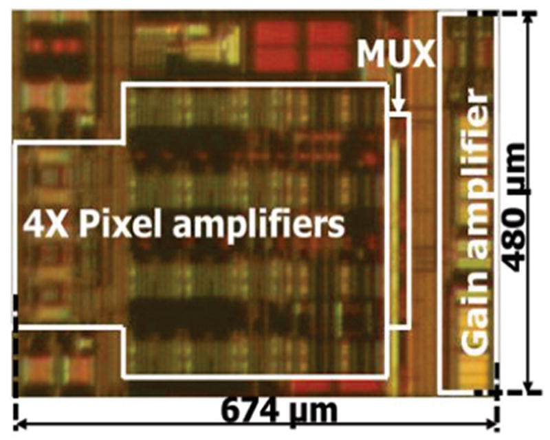
Chip photo of one cluster amplifier with four pixels. The active area per channel is 0.06 mm2, allowing over 100 channels in a 2.5 × 2.5 mm2 area.
The chip was powered by an ultra-low noise 3.3 V voltage regulator on a custom printed circuit board (PCB) built to characterize the chip. Key analog signal traces on the 4-layer PCB were surrounded by grounded traces to provide shielding of 60-Hz line noise and other environmental noise. A Faraday cage was used to provide additional noise suppression. A data acquisition card (NI USB-6259, National Instruments) was used for data digitization, and LabVIEW (National Instruments) was used to configure the data acquisition card and display, record, and store test results.
A. Electrical Characterization
To characterize the pixel amplifier’s input current range, a Keithley 6430 ultra-low noise current generator was used to generate different DC input currents. The feedback resistance Rf in the on-chip signal processing stage I/V convertor can limit input currents, and to evaluate the Rf effect on input current range, Rf was set at 1 MΩ and 10 MΩ. The input current ranges for these two resistance values are shown in Fig. 12. When Rf = 10 MΩ, the input current range is -9 to 20 nA with output error less than 3%. When the input current is out of range, the output voltage reaches the supply rails of 0 V or 3.3 V, which limits the input range. When Rf = 1 MΩ, the input current range is -110 to 90 nA with output error less than 1%. Larger Rf values produces higher resolution by providing larger gain but produces smaller input current range.
Fig. 12.
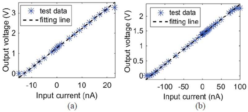
DC response test result of pixel amplifier when (a) Rf=10 MΩ and (b) Rf=1 MΩ.
To characterize the pixel amplifier’s AC response, a waveform generator (ETabor Electronics) was used to generate a sinusoid voltage signal that was applied across a resistor to generate an input sinusoid current with power of Spower. The frequency was swept from 50 Hz to 19 kHz, and the corresponding channel’s output power Rpower was recorded by an Agilent 4395A spectrum analyzer. The circuit’s bandwidth response plot obtained from is shown in Fig. 13 (a). The pixel amplifier has a low-frequency gain of 19.7 dB (9.7×) and a bandwidth of 11.5 kHz, created by the external LPF. Without the external LPF, the circuit’s bandwidth is 16 kHz. During the AC response test, another channel’s response power Rcrosstalk was recorded to measure crosstalk defined as Rcrosstalk/Rpower. The crosstalk test result and corresponding fitting curve are shown in Fig. 13 (b), demonstrating the crosstalk is -38.2 dB at 10 kHz.
Fig. 13.
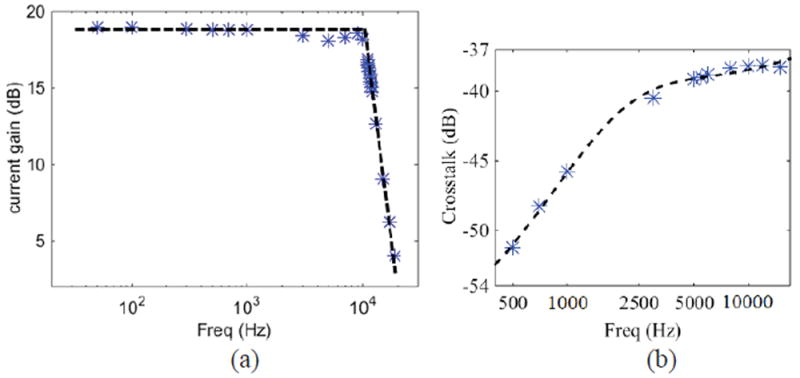
AC response test results of pixel amplifier: (a) gain response results, and (b) crosstalk response Rcrosstalk/Rpower results. Asterisk markers represent test data, and dashed line represents the fitting line.
To demonstrate the transient response of the two-stage circuit, the on-chip self-test current pulse generator produced a current pulse with amplitude Iamp=105 pA and pulse width Twidth =1 ms, as defined in Fig. 9. The circuit response output is shown in Fig. 14 where a low-pass filter (LPF) with cut-off frequency at 11.5 kHz was used to post-process the response data in Matlab. To characterize the noise response of the two-stage circuit, Rf was set to 100 MΩ, the input current was set at zero and the transient response was recorded. The same LPF in Matlab was used to post-process the data. Fig. 14 gives the peak-to-peak Vpk-pk value at the plateau region around 14 ms. Based on definition in [42], the output voltage noise Vo_rms is Vpk-pk/8. The input equivalent current noise is Vo_rms/Aν, where Aν is the current gain. As a result, the measured RMS noise was 7.2 pArms in 11.5 kHz bandwidth. The circuit’s performance is summarized and compared to other work in Table IV. The reported circuit has superior performance in power and area, and all other performance factors meet the biosensor array requirements.
Fig. 14.
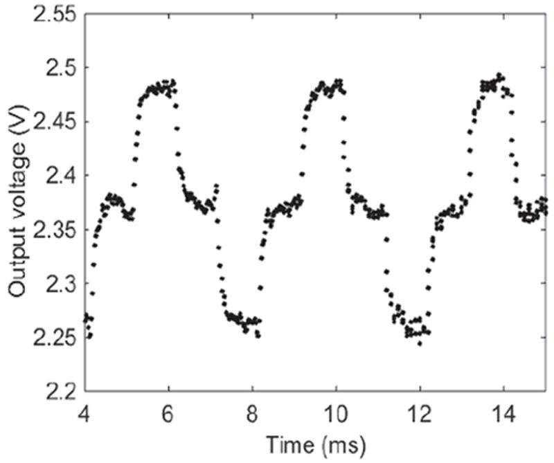
Transient current response of the two-stage circuit when Iamp = 105 pA and Iwidth = 1 ms.
TABLE IV.
COMPARISONS TO PREVIOUS WORK ON ELECTROCHEMICAL BIOSENSORS CURRENT READOUTS
| This work | [16] | [24] | [25] | [33] | [20] | |
|---|---|---|---|---|---|---|
| Power/chan. (μW) | 21 | 300 | 1500 | 5000 | 130 | 241 |
| Area/chan. (mm2) | 0.06 | 0.81 | 0.28 | 0.4 | - | 0.22 |
| BW. (Hz) | 11.5k | - | - | 1M | <1 | <100 |
| Noise over BW. (Arms) | 7.2p in 11.5kHz BW | 5p in 10kHz BW | 2.4p in 10kHz BW | 61p in 1MHz BW | <1p in 1Hz BW | <100f in <100Hz BW |
| Max. current (nA) | -110, 90 | ±20 | -12, 13 | >18 | 200 | 16000 |
| Process (μm) | 0.5 | 0.5 | 0.5 | 0.13 | 0.5 | 0.5 |
B. Electrochemical Experiments
Cyclic voltammetry (CV) is an electrochemical method, widely used in electrochemical biosensor development. This method applies a triangle stimulation voltage to the biosensor and records the response current to study the electrochemical response. Potassium ferricyanide (K4[Fe(CN)6]) solution is a commonly used electrolyte for electrochemical experiments. 100 μM K4[Fe(CN)6] with a 0.1M KCL buffer solution was used to validate the circuit’s performance with an electrochemical interface. The CV test platform is shown in Fig. 15. For this redox-reaction based system, three-electrode setup is better than two-electrode setup due to better control of the chemical reaction process [18, 37].
Fig. 15.
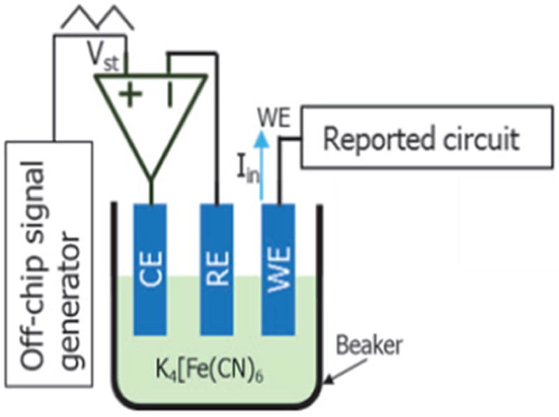
CV test setup.
A three-electrode electrochemical system was setup by using a 211 μm × 214 μm off-chip gold microelectrode as working electrode (WE), a Ag-AgCl electrode (CHI Instruments, Inc.) as reference electrode (RE), and a Pt electrode (CHI Instruments, Inc.) as counter electrode (CE). An off-chip, discrete control amplifier was used to drive the RE and CE. The voltage between RE and WE was swept from -0.5 V to 0 V at different scan rates, including 10, 20, 30, 40 mV/s. Due to the large signal magnitude, gain amplifier is off, and only pixel amplifier is used for recording. A zero-phase, low pass FIR filter was used to post-process the response data in Matlab. Fig. 16 (a) shows that the resulting reduction and oxidation current peaks are at -0.186 V and -0.25 V, respectively. The 64 mV peak potential difference is very close to the theoretical value of 59 mV for a fully reversible, single-electron redox process [37]. Fig. 16 (b) plots the oxidation peak current vs. the square root of scan rate and shows that the expected linear relationship was obtained with R-square error of 0.98. The oxidation peak current was defined as the current at -0.25 V after subtracting charging current calculated in the nonfaradaic response[37].
Fig. 16.
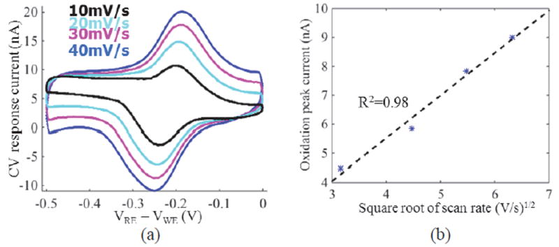
(a). CV test result of 100 μM K4[Fe(CN)6] solution at different scan rates using a 0.045 mm2 gold electrode, and (b) corresponding relation between oxidation peak current and scan rate. In (b), the asterisk markers represent test data, and the dashed line represents the fitting line.
C. Biological Experiments
To demonstrate the circuit’s ability to interface with a biological sample, cell membrane impedance was measured using off-chip whole-cell patch clamp experiments. Cell membranes can be modeled as a resistor in parallel with a capacitor, and membrane resistance and capacitance can be readily measured using the whole-cell configuration of patch clamp electrophysiology [43]. Changes in passive membrane properties, such as membrane resistance and capacitance, can be interpreted as an indicator of important cellular events such as maturation, morphological changes, alterations in ion channel expression responsible for determining cellular excitability, and changes in cell health [44-46]. Given the close relationship with cellular physiology, measurement of passive membrane properties can be utilized in a variety of biomedical applications including toxin detection and drug screening [17].
The setup of whole-cell patch clamp experiments is shown in Fig. 17, where a two-electrode system is used because no chemical reaction necessitating a third electrode occur. Cells were placed in an external solution that mimics the extracellular milieu of the in vivo environment. A glass capillary was heat-pulled to a fine tip to seal onto the cell membrane. The pipette contains an internal solution that dialyzes with the intracellular compartment following breakage of the small patch of membrane between the electrode and cell. For this study, primary cortical neurons isolated from embryonic rats onto plastic coverslips (Thermanox) were cultured according to the supplier’s protocol (Life Technologies). The external solution was an oxygenated physiological saline solution containing (in mM) 126 NaCl, 2.5 KCl, 1.25 NaH2PO4, 2 CaCl2 2H2O, 2 MgSO4 7H2O, 26 NaHCO3, and 10 Glucose. Borosilicate glass pipettes were fabricated with a pipette puller (Sutter Instruments) and filled with internal solution (in mM) of 135 K Gluconate, 7 NaCl, 10 HEPES, 2 MgCl2, 2 Na2ATP, and 0.3 Na2GTP. Once the pipette was properly affixed to the patch clamp micromanipulator (Narishige), primary cortical neurons were approached, sealed, and recorded using our fabricated CMOS current readout chip.
Fig. 17.
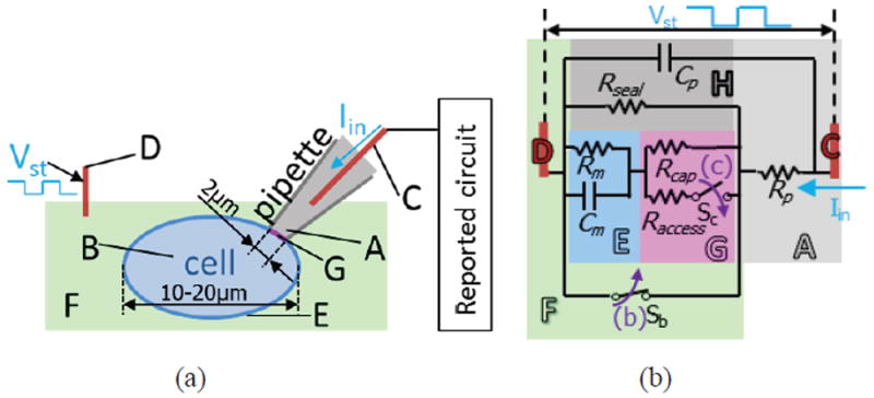
(a) Whole-cell patch clamp test setup and (b) electrical circuit modeling the successive patch-clamp procedures, adapted from [42]. A: pipette internal solution, B: cell cytoplasm, C: electrode 1, D: electrode 2, E: cell membrane, F: external solution (bath), G: cell patch in pipette, H. pipette edge. Rp and Cp are the pipette resistance and capacitance, respectively. Rm and Cm are the cell membrane resistance (due to ion channel) and cell capacitance, respectively. Rseal is the leak resistance and represents the quality of the seal between the pipette and membrane. Rcap is the cell-attached patch resistance inside the pipette tip. Raccess is the access resistance after the cell-attached patch is broken, representing the access to the inside of the whole cell. Rcap, Rseal ≫ Raccess, Rm. In (b), switch Sb and Sc represent patch-clamp procedures' equivalent actions in the circuit model.
To measure the cell membrane impedance, 100 Hz voltage pulses Vst were applied at the external solution electrode following established methods [43], where pulse amplitudes were kept small enough to avoid damaging the cell and large enough to provide good signal-to-noise ratio. The pipette electrode voltage was set at VWE by the reported circuit. The response current pulses during key stages of the test procedure were recorded and are shown in Fig. 18. The currents are associated with the ion flow path between the pipette internal solution and external solution. The monitored resistance was calculated from Vpp/Ipp, where Vpp and Ipp are the peak-to-peak value of applied voltage pulse and recorded current pulse, respectively. In Fig. 18 (a), the pipette is in the external solution and does not touch the cell. The ions can freely flow between the pipette internal solution and external solution under voltage stimulation. As a result, a large (nA-level) current pulse was observed. The monitored resistance is called “pipette resistance”. In Fig. 18 (b), the pipette firmly touches the cell membrane and negative pressure is applied inside the pipette, which pulls the cell membrane toward the pipette. As a result, the ion flow path between internal and external solution is so narrow that only very small (pA-level) current could be generated, corresponding to gigaohm resistance. This procedure is called “gigaseal”. In Fig. 18 (c), the negative pressure inside the pipette is increased causing breakage of the cell membrane patch inside the pipette. The ions inside of the pipette internal solution flow through the cell membrane and generate a larger current response. The monitored resistance is equal to the cell membrane resistance plus the pipette resistance.
Fig. 18.
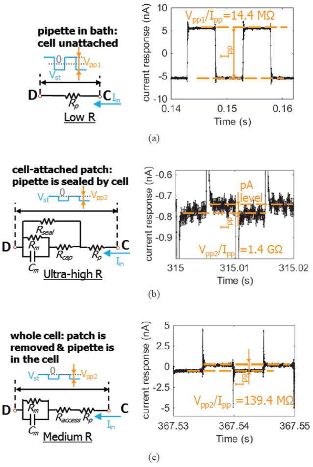
Equivalent circuit model during key experimental procedures: (a) pipette tip in bath: when the pipette tip is contacting the external solution and does not touch cell membrane; (b) cell-attached patch: when the pipette tip is touching the cell membrane and negative pressure is applied inside the pipette to pull cell membrane against pipette tip to form a seal between the pipette and membrane; (c) whole cell: when the cell patch inside the pipette tip is ruptured by larger negative pressure present inside the pipette to measure cell impedance.
Vpp was set at 160 mV for the measurement in Fig. 18 (a). Vpp was reduced to 70 mV and the offset was set at -35 mV for the measurements in Fig. 18 (b) and (c) to mitigate the potential for overstimulation and excitotoxicity. The spikes in Fig. 18 (b) and (c) shows capacitive transients in response to voltage pulses upon contact between the pipette and cell membrane [43]. Fig. 18 (b) and (c) show offset currents due to the stimulation voltage offset. To accurately measure the gigaseal resistance, a low-pass filter with cut-off frequency at 1 kHz was used to post-process the raw recorded data in Matlab. The calculated resistances for all the test procedures match very well to theoretical values, as listed in Table V. Our system repeated the biological interface measurements in Fig. 18 (a) and Fig 18 (b) more than five times with similar results. These two results require high circuit noise performance and demonstrate the circuit’s capability to measure over 1 GΩ passive membrane resistance. Furthermore, these patch clamp electrophysiology results suggest that the reported circuit is suitable for use with sensors that identify changes in cell health, excitability, and membrane integrity in response to varying environmental conditions. The results in Fig 18 (c) are biologically relevant but require a well-trained operator working under the time constraints of the cell’s lifetime (~1 hour). Moreover, they do not push the circuit’s performance limits. Thus, the measurements in Fig. 18(c) were only performed once.
Table V.
RECORDED RESISTANCE VS. THEORETICAL VALUES FOR WHOLE-CELL EXPERIMENTS PROCEDURES
| Experiment procedures | Resistance | |
|---|---|---|
| Tested | Theoretical | |
| Fig. 18 (a) | 14.4 MΩ (pipette resistance) | 10-15 MΩ (empirical value) |
| Fig. 18 (b) | 1.4 GΩ (gigaseal resistance) | >1 GΩ [42] |
| Fig. 18 (c) | 139.4 MΩ (membrane resistance) | ~100-200 MΩ [45] |
VII. Conclusion
This paper presents a new CMOS readout circuit for electrochemical biosensor arrays that simultaneously provides good noise performance and bandwidth while achieving very low power consumption and small circuit size. The new pixel-level current readout circuit and new group-cluster system architecture significantly reduce the circuit power and area without compromising other performance requirements. Noise analysis was presented for design optimization. Circuit characterization results show that circuit achieves 7.5 pArms noise in 11.5 kHz bandwidth and over 90 nA bidirectional input current range while only consuming 21 μW power and 0.06 mm2 area per channel. Electrochemical CV experiments and patch-clamp whole-cell experiments validate the circuit’s feasibility for many biosensor applications.
Acknowledgments
Thanks to Lin Li and Heyu Yin for microelectrode fabrication.
This work was supported by National Science Foundation (NSF) grant ECCS-1307939, and National Institutes of Health (NIH) R01ES022302.
References
- 1.Wilkins E, Atanasov P. Glucose monitoring: state of the art and future possibilities. Medical engineering & physics. 1996;18:273–288. doi: 10.1016/1350-4533(95)00046-1. [DOI] [PubMed] [Google Scholar]
- 2.Schena M. DNA microarrays: a practical approach. Oxford university press; 1999. [Google Scholar]
- 3.Trojanowicz M. Miniaturized biochemical sensing devices based on planar bilayer lipid membranes. Fresenius’ journal of analytical chemistry. 2001;371:246–260. doi: 10.1007/s002160101005. [DOI] [PubMed] [Google Scholar]
- 4.Ahmed MU, Hossain MM, Tamiya E. Electrochemical biosensors for medical and food applications. Electroanalysis. 2008;20:616–626. [Google Scholar]
- 5.Lillehoj PB, Huang M-C, Truong N, et al. Rapid electrochemical detection on a mobile phone. Lab on a Chip. 2013;13:2950–2955. doi: 10.1039/c3lc50306b. [DOI] [PubMed] [Google Scholar]
- 6.Li H, Parsnejad S, Mason AJ. Single ion channel CMOS electrochemical instrument for high throughput recording arrays. Circuits and Systems (MWSCAS), IEEE 58th International Midwest Symposium on; Fort Collins, Colorado. 2015. [Google Scholar]
- 7.Li H, Mu X, Yang Y, et al. Low power multi-mode electrochemical gas sensor array system for wearable health and safety monitoring. Sensors Journal, IEEE. 2014;14:3391–3399. [Google Scholar]
- 8.Vidal JC, Bonel L, Ezquerra A, et al. Electrochemical affinity biosensors for detection of mycotoxins: A review. Biosensors and Bioelectronics. 2013;49:146–158. doi: 10.1016/j.bios.2013.05.008. [DOI] [PubMed] [Google Scholar]
- 9.Hashimoto K, Ito K, Ishimori Y. Microfabricated disposable DNA sensor for detection of hepatitis B virus DNA. Sensors and Actuators B: Chemical. 1998;46:220–225. [Google Scholar]
- 10.Aguilar Z, Narasimhan PY, Wansapura C, et al. Electrochemical Immunoassay Detection of Bacillus Anthracis Protective Antigen. ECS Transactions. 2008;13:1–15. [Google Scholar]
- 11.Skládal P. Advances in electrochemical immunosensors. Electroanalysis. 1997;9:737–745. [Google Scholar]
- 12.Muhammad-Tahir Z, Alocilja EC. Fabrication of a disposable biosensor for Escherichia coli O157: H7 detection. Sensors Journal, IEEE. 2003;3:345–351. [Google Scholar]
- 13.Viswanathan S, Wu L, Huang M, et al. Electrochemical immunosensor for cholera toxin using liposomes and poly (3, 4-ethylenedioxythiophene)-coated carbon nanotubes. Analytical Chemistry. 2006;78:1115–1121. doi: 10.1021/ac051435d. [DOI] [PubMed] [Google Scholar]
- 14.Liu X, Li L, Mason AJ. High throughput single-ion-channel array microsystem with CMOS instrumentation. Engineering in Medicine and Biology Society (EMBC), 2014 36th Annual International Conference of the IEEE; 2014. pp. 2765–2768. [DOI] [PubMed] [Google Scholar]
- 15.Li L, Mason A. Development of an integrated CMOS-microfluidic instrumentation array for high throughput membrane protein studies. Circuits and Systems (ISCAS), 2014 IEEE International Symposium on; 2014. pp. 638–641. [Google Scholar]
- 16.Weerakoon P, Culurciello E, Klemic KG, et al. An integrated patch-clamp potentiostat with electrode compensation. Biomedical Circuits and Systems, IEEE Transactions on. 2009;3:117–125. doi: 10.1109/TBCAS.2008.2005419. [DOI] [PubMed] [Google Scholar]
- 17.Du E, Ha S, Diez-Silva M, et al. Electric impedance microflow cytometry for characterization of cell disease states. Lab on a Chip. 2013;13:3903–3909. doi: 10.1039/c3lc50540e. [DOI] [PMC free article] [PubMed] [Google Scholar]
- 18.Li H, Liu X, Li L, et al. CMOS Electrochemical Instrumentation for Biosensor Microsystems: A Review. Sensors. 2016;17:74. doi: 10.3390/s17010074. [DOI] [PMC free article] [PubMed] [Google Scholar]
- 19.Huang Y, Mason AJ. Lab-on-CMOS integration of microfluidics and electrochemical sensors. Lab on a Chip. 2013;13:3929–3934. doi: 10.1039/c3lc50437a. [DOI] [PMC free article] [PubMed] [Google Scholar]
- 20.Li H, Boling CS, Mason AJ. CMOS amperometric ADC with high sensitivity, dynamic range and power efficiency for air quality monitoring. Biomedical Circuits and Systems, IEEE Transactions on. 2016;10:817–827. doi: 10.1109/TBCAS.2016.2571306. [DOI] [PMC free article] [PubMed] [Google Scholar]
- 21.Gore A, Chakrabartty S, Pal S, et al. A multichannel femtoampere-sensitivity potentiostat array for biosensing applications. Circuits and Systems I: Regular Papers, IEEE Transactions on. 2006;53:2357–2363. [Google Scholar]
- 22.Jafari H, Soleymani L, Genov R. 16-channel CMOS impedance spectroscopy DNA analyzer with dual-slope multiplying ADCs. Biomedical Circuits and Systems, IEEE Transactions on. 2012;6:468–478. doi: 10.1109/TBCAS.2012.2226334. [DOI] [PubMed] [Google Scholar]
- 23.Nazari MH, Mazhab-Jafari H, Leng L, et al. CMOS neurotransmitter microarray: 96-channel integrated potentiostat with on-die microsensors. Biomedical Circuits and Systems, IEEE Transactions on. 2013;7:338–348. doi: 10.1109/TBCAS.2012.2203597. [DOI] [PubMed] [Google Scholar]
- 24.Goldstein B, Kim D, Xu J, et al. CMOS low current measurement system for biomedical applications. Biomedical Circuits and Systems, IEEE Transactions on. 2012;6:111–119. doi: 10.1109/TBCAS.2011.2182512. [DOI] [PubMed] [Google Scholar]
- 25.Rosenstein JK, Ramakrishnan S, Roseman J, et al. Single ion channel recordings with CMOS-anchored lipid membranes. Nano letters. 2013;13:2682–2686. doi: 10.1021/nl400822r. [DOI] [PMC free article] [PubMed] [Google Scholar]
- 26.Jafari HM, Genov R. Chopper-stabilized bidirectional current acquisition circuits for electrochemical amperometric biosensors. Circuits and Systems I: Regular Papers, IEEE Transactions on. 2013;60:1149–1157. [Google Scholar]
- 27.Seese TM, Harasaki H, Saidel GM, et al. Characterization of tissue morphology, angiogenesis, and temperature in the adaptive response of muscle tissue to chronic heating. Laboratory investigation; a journal of technical methods and pathology. 1998;78:1553–1562. [PubMed] [Google Scholar]
- 28.Levine PM, Gong P, Levicky R, et al. Active CMOS sensor array for electrochemical biomolecular detection. Solid-State Circuits, IEEE Journal of. 2008;43:1859–1871. [Google Scholar]
- 29.Yang C, Huang Y, Hassler BL, et al. Amperometric electrochemical microsystem for a miniaturized protein biosensor array. Biomedical Circuits and Systems, IEEE Transactions on. 2009;3:160–168. doi: 10.1109/TBCAS.2009.2015650. [DOI] [PubMed] [Google Scholar]
- 30.Rosenstein JK, Wanunu M, Merchant CA, et al. Integrated nanopore sensing platform with sub-microsecond temporal resolution. Nature methods. 2012;9:487–492. doi: 10.1038/nmeth.1932. [DOI] [PMC free article] [PubMed] [Google Scholar]
- 31.Crescentini M, Bennati M, Carminati M, et al. Noise limits of CMOS current interfaces for biosensors: A review. Biomedical Circuits and Systems, IEEE Transactions on. 2014;8:278–292. doi: 10.1109/TBCAS.2013.2262998. [DOI] [PubMed] [Google Scholar]
- 32.Liu X, Li H, Yin L, et al. Noise analysis and characterization of a full differential CMOS interface circuit for capacitive closed-loop micro-accelerometer. Journal of Harbin Institute of Technology. 2010;17:684–689. [Google Scholar]
- 33.Narula HS, Harris JG. A time-based VLSI potentiostat for ion current measurements. Sensors Journal, IEEE. 2006;6:239–247. [Google Scholar]
- 34.Genov R, Stanacevic M, Naware M, et al. 16-channel integrated potentiostat for distributed neurochemical sensing. Circuits and Systems I: Regular Papers, IEEE Transactions on. 2006;53:2371–2376. [Google Scholar]
- 35.Ayers S, Gillis KD, Lindau M, et al. Design of a CMOS potentiostat circuit for electrochemical detector arrays. Circuits and Systems I: Regular Papers, IEEE Transactions on. 2007;54:736–744. doi: 10.1109/TCSI.2006.888777. [DOI] [PMC free article] [PubMed] [Google Scholar]
- 36.Hastings A. The art of analog layout. Prentice Hall; 2006. [Google Scholar]
- 37.Bard AJ, Faulkner LR. Electrochemical methods: fundamentals and applications. Vol. 2. Wiley; New York: 2000. [Google Scholar]
- 38.Chae MS, Liu W, Sivaprakasam M. Design optimization for integrated neural recording systems. Solid-State Circuits, IEEE Journal of. 2008;43:1931–1939. [Google Scholar]
- 39.Linares-Barranco B, Serrano-Gotarredona T. On the design and characterization of femtoampere current-mode circuits. Solid-State Circuits, IEEE Journal of. 2003;38:1353–1363. [Google Scholar]
- 40.Razavi B. Design of analog CMOS integrated circuits. McGraw-Hill; 2003. [Google Scholar]
- 41.Johns D, Martin K. Analog Integrated Circuit Design. Wiley; 1997. [Google Scholar]
- 42.http://mdc.custhelp.com.
- 43.Molleman A. Patch clamping: an introductory guide to patch clamp electrophysiology. John Wiley & Sons; 2003. [Google Scholar]
- 44.Hamill OP, Marty A, Neher E, et al. Improved patch-clamp techniques for high-resolution current recording from cells and cell-free membrane patches. Pflügers Archiv. 1981;391:85–100. doi: 10.1007/BF00656997. [DOI] [PubMed] [Google Scholar]
- 45.Purcell EK, Yang A, Liu L, et al. BDNF profoundly and specifically increases KCNQ4 expression in neurons derived from embryonic stem cells. Stem cell research. 2013;10:29–35. doi: 10.1016/j.scr.2012.08.005. [DOI] [PMC free article] [PubMed] [Google Scholar]
- 46.Magnuson DS, Morassutti DJ, Staines WA, et al. In vivo electrophysiological maturation of neurons derived from a multipotent precursor (embryonal carcinoma) cell line. Developmental brain research. 1995;84:130–141. doi: 10.1016/0165-3806(94)00166-w. [DOI] [PubMed] [Google Scholar]


