Abstract
Purpose
We present the first prototype Scintillator High‐Gain Avalanche Rushing Photoconductor Active Matrix Flat Panel Imager (SHARP‐AMFPI). This detector includes a layer of avalanche amorphous Selenium (a‐Se) (HARP) as the photoconductor in an indirect detector to amplify the signal and reduce the effects of electronic noise to obtain quantum noise‐limited images for low‐dose applications. It is the first time avalanche a‐Se has been used in a solid‐state imaging device and poses as a possible solution to eliminate the effects of electronic noise, which is crucial for low‐dose imaging performance of AMFPI.
Methods
We successfully deposited a solid‐state HARP structure onto a 24 × 30 cm2 array of thin‐film transistors (TFT array) with a pixel pitch of 85 μm. The HARP layer consists of 16 μm of a‐Se with a hole‐blocking and electron‐blocking layer to prevent charge injection from the high‐voltage bias and pixel electrodes, respectively. An electric field ( E S e ) up to 105 V μm−1 was applied across the a‐Se layer without breakdown. A 150 μm thick‐structured CsI:Tl scintillator was used to form SHARP‐AMFPI. The x‐ray imaging performance is characterized using a 30 kVp Mo/Mo beam. We evaluate the spatial resolution, noise power, and detective quantum efficiency at zero frequency of the system with and without avalanche gain. The results are analyzed using cascaded linear system model (CLSM).
Results
An avalanche gain of 76 ± 5 was measured at E S e = 105 V μm−1. We demonstrate that avalanche gain can amplify the signal to overcome electronic noise. As avalanche gain is increased, image quality improves for a constant (0.76 mR) exposure until electronic noise is overcome. Our system is currently limited by poor optical transparency of our high‐voltage electrode and long integrating time which results in dark current noise. These two effects cause high‐spatial frequency noise to dominate imaging performance.
Conclusions
We demonstrate the feasibility of a solid‐state HARP x‐ray imager and have fabricated the largest active area HARP sensor to date. Procedures to reduce secondary quantum and dark noise are outlined. Future work will improve optical coupling and charge transport which will allow for frequency DQE and temporal metrics to be obtained.
Keywords: avalanche gain, digital detectors, selenium, solid state
1. Introduction
1.A. Limitations of existing flat‐panel imagers at low dose
Active Matrix Flat Panel Imagers (AMFPI) have revolutionized medical imaging due to their high image quality and real‐time readout capabilities.1, 2 In an indirect AMFPI, a scintillator is used to convert x rays to optical photons, which are then detected by an array of pixelated amorphous silicon photodiodes, and generate electron–hole pairs (EHPs). The charge image is read out using an array of amorphous silicon thin‐film transistors (TFTs). Indirect detectors are widely used for fluoroscopy and general radiography due to their higher quantum efficiency afforded by the structured Cesium iodide activated with Thallium (herein referred to as CsI) scintillators. Unfortunately, the indirect AMFPI suffers from reduced image performance at low dose. Based on pixel pitch (a p ) and x‐ray energy, we consider low dose to be a detector exposure of <0.1 μR for fluoroscopy and <1 mR for mammography. At these exposures, the pixel electronic noise (S n ) degrades image quality.3, 4 Two solutions have been proposed to overcome the degradation effects of S n while maintaining the use of the TFT array. The first is to reduce S n of the TFT array, and the second is to amplify the signal with photoconductive avalanche gain (g av ).
Active pixel sensor (APS) designs have been proposed as a strategy to reduce S n . These designs incorporate additional transistors at each pixel to reduce the S n by up to a factor of two.5, 6, 7, 8 However, APS does not completely eliminate the degradation of image quality and adds substantial cost to manufacturing. In this work, we use g av in amorphous selenium (a‐Se) to amplify the signal in the photoconductor before charge storage in the pixel capacitor. Avalanche gain potentially overcomes the effects of S n at all spatial frequencies while using identical readout electronics to those used in the existing direct AMFPI. We present the first image sensor to incorporate a solid‐state avalanche a‐Se layer called High‐Gain Avalanche Rushing Photoconductor (HARP) as the optical sensing layer in an indirect AMFPI.
1.B. Scintillator high‐gain avalanche rushing photoconductor AMFPI
The indirect detector presented in this work is referred to as Scintillator HARP (SHARP)‐AMFPI (Fig. 1).9, 10, 11 A HARP layer is deposited directly onto a TFT array, and a scintillator is then coupled to the optical HARP structure to complete the indirect detector. Amplification of the photoconductive signal prior to image readout by the TFT array will eliminate the degradation effect of electronic noise for imaging performance at low dose. It has previously been demonstrated that a g av of 10–20 should be sufficient to achieve x‐ray quantum noise‐limited images for most medical applications.9
Figure 1.

Cross section of SHARP‐AMFPI detector. Optical photons generated from a scintillator are converted to EHPs in the a‐Se and undergo avalanche multiplication providing nearly noiseless signal gain to overcome electronic noise. Thicknesses not drawn to scale.
1.C. Avalanche gain in a‐Se
Amorphous materials have the advantage of large area deposition compared to their crystalline counterparts, and the only amorphous semiconductor capable of avalanche gain is a‐Se. With an applied electric field in selenium (E Se ) > 70 V μm−1, holes undergo impact ionization to produce additional EHPs thereby amplifying the signal. The magnitude of g av is determined by the impact ionization coefficient, α, given by the empirical formula:12
| (1) |
The parameters, α 1 and α 2 , are experimentally fitted. The magnitude of g av also depends on the thickness D of a‐Se:
| (2) |
To achieve g av = 10 required for medical imaging applications, an E Se of 92 V μm−1 (with D = 15 μm) is needed. To maintain a moderate bias voltage (Vb < 3000 V), the thickness of a‐Se is generally limited to 8–15 μm but can range from 1 to 30 μm.13, 14 To maintain E Se = 90 V μm−1 reliably, the a‐Se layer must be isolated from the positive and negative bias electrodes by a hole‐blocking (n‐type semiconductor) and electron‐blocking (p‐type) layer, respectively, to prevent charge injection. Without blocking layers, dark current increases substantially at high E Se , which would produce Joule heating resulting in crystallization of the a‐Se and permanent material damage.15 This multilayer blocking structure is crucial for practical success of HARP technology with minimal dark current.16
HARP was first commercialized over two decades ago17 in a vacuum tube‐based optical imaging camera. The sensor was fabricated on an ITO‐coated glass substrate utilizing an n‐i‐p deposition sequence and a scanning electron beam readout with a one inch diameter active area.18 Solid‐state HARP requires the reverse deposition in a p‐i‐n sequence. This structure is substantially more difficult to fabricate due to the lack of hole‐blocking layers with room temperature deposition capabilities. Since only holes undergo avalanche multiplication, the hole injection is far more critical than the electron injection. Materials that require an elevated substrate or curing temperature during deposition will raise the temperature of the a‐Se above its glass transition, which leads to recrystallization. As a‐Se crystalizes, the band gap decreases and the conductivity increases thereby shorting the HV bias and pixel electrodes. Several attempts have been made to create a solid‐state detector using an n‐i‐p sensor including electroded HARP19 and a HARP layer coupled to a CMOS sensor through indium bump bonding;20 however, both methods are impractical for the fabrication of an AMFPI. Recently, we successfully developed the p‐i‐n HARP structure, which was the first solid‐state HARP layer scalable to large area.21 This p‐i‐n HARP structure can be deposited directly onto a TFT array to create a highly sensitive optical sensor and SHARP‐AMFPI with an optically coupled scintillator (Fig. 1).
2. Materials and methods
2.A. Prototype detector fabrication
Our HARP structure21 was deposited on to a TFT array with a pixel pitch of 85 μm and a total active area of 24 × 30 cm2. The HARP layer structure is shown in Fig. 2(a) and the top view of the detector is shown in Fig. 2(b). First, a 2 μm thick inorganic electron‐blocking layer was thermally deposited directly onto the TFT array. A 16 μm thick layer of intrinsic stabilized a‐Se was then deposited followed by a 2 μm thick layer of a wide bandgap organic polymer to act as the hole‐blocking layer. The high‐voltage (HV) electrode was a thin layer of semitransparent chromium (Cr). Multiple HV electrodes ranging from 1 × 1 cm2 to 9 × 7 cm2 were deposited, thereby allowing each region to be tested separately to minimize damage associated with possible breakdown. The entire detector structure was encapsulated with 20 μm of an organic dielectric which improves the detector stability. The SHARP‐AMFPI was completed by incorporating a 150 μm structured CsI scintillator with a fiber optic faceplate (FOP) and reflective backing (FOS 150 HL, Hamamatsu Photonics K.K., Shizuoka, Japan). This combination of pixel size and CsI thickness is well suited for breast imaging due to the high‐spatial resolution and high detection efficiency of the scintillator. Foam compression was used between the top of the scintillator and the detector housing to improve the optical coupling between the scintillator and HARP layer. The FOP attenuates over 99% of the x rays at mammographic energies; thus, direct x‐ray interactions can be neglected.9 The detector was housed in a standard mammography cassette with a carbon fiber cover.22
Figure 2.

(a) Cross section of multilayer HARP structure (not to scale). (b) Top view of the 24 × 30 cm2 TFT array covered with a continuous layer of avalanche a‐Se. Multiple HV electrodes were used to assess gain uniformity while minimizing risk of breakdown. The scintillator is not shown. [Color figure can be viewed at wileyonlinelibrary.com]
2.B. SHARP‐AMFPI evaluation
The x‐ray imaging performance of the SHARP‐AMFPI is characterized with an IMS Giotto imaging system using a 30 kVp Mo/Mo x‐ray beam (0.47 mm HVL). The bias voltage (V b ) was applied via a HV power supply (PS350, Stanford Research Systems, Sunnyvale, CA, USA) with a 2 MΩ output resistance in series to minimize ripples in the V b . The integration window was ~2 s and the frame rate was 0.2 Hz. For sensitivity measurements, the offset‐corrected frame was averaged over a ~1 cm2 area in a region without visible defects. In this first prototype detector, the electron transport through the hole‐blocking layer has not yet been optimized. Electrons trapped at the interface between the a‐Se and hole‐blocking layer could reduce the E se and x‐ray sensitivity in subsequent frames, that is, ghosting.23 Thus, between each measurement, V b was removed and uniform light exposure from a built‐in light source behind the TFT array was used to eliminate any trapped charge and its associated ghosting artifacts.
The sensitivity of SHARP‐AMFPI as a function of E Se was evaluated. The modulation transfer function (MTF), noise power spectrum (NPS), and detective quantum efficiency (DQE) of the system were measured at E Se = 10 V μm−1 and 90 V μm−1 (g av = 7). E Se = 90 V μm−1 is used since it provides a gain of ~10 required by a properly optimized system. The MTF was measured using the slanted edge technique with a tungsten edge.24 The 2D NPS was calculated using an ROI of 320 × 230 pixels which was limited by the size of the CsI scintillator used. Dead pixels were identified as having a gain value greater than 5× the standard deviation of the mean gain. The maximum number of dead pixels within the ROI is one and four at E Se = 10 and 90 V μm−1, respectively. The defective pixels were corrected using the mean of the four neighboring pixels. The offset and gain table were computed using the average of ten frames to reduce additional noise, and they were used to correct the images before calculating sensitivity, MTF, and NPS.
Finally, x‐ray images were acquired with the prototype SHARP‐AMFPI with and without g av . The first object was a Canadian penny with the heads side removed which allowed for easy visual assessment of image quality. Images were acquired at E Se ranging from 15 to 105 V μm−1 with an exposure of 0.76 mR which is equivalent to 1/15 of the mean detector exposure behind the breast in screening mammography.25 Then, x‐ray images were also acquired at E Se = 105 V μm−1 with exposure levels incrementally reduced to as low as 0.02 mR. The second object was the CIRS BR3D breast‐imaging phantom to provide visual comparison of image quality with avalanche gain using a tissue‐like phantom. For all images, only an offset correction was performed on each frame (without gain or dead pixel corrections) to demonstrate the uniformity in g av on a pixel by pixel level.
2.C. Cascaded linear system model (CLSM) for SHARP‐AMFPI
A cascaded linear system model (CLSM) was previously developed for SHARP‐AMFPI to understand the factors affecting DQE, which is given by:9
| (3) |
where T b (f), T c (f), and T a (f) are the MTF of the scintillator, the optical coupling between the scintillator and the HARP, and the pixel aperture function, respectively. The scintillator performance is characterized by its x‐ray quantum efficiency (η), the Swank factor A S , and the x ray to optical photon conversion gain g (optical photons/x‐ray photon). The optical coupling efficiency between CsI and HARP layer is given by δ. The performance of HARP is characterized by its optical quantum efficiency γ and the avalanche gain g av . Finally, a p is the pixel aperture and q 0 is the number of x‐ray quanta per mm2. The electronic noise power density is given by S n (e2 mm2). The first term in the denominator represents the x‐ray quantum noise. The second term represents the secondary quantum noise, which depends on the characteristics of various gain stages. The final term represents the effect of electronic noise. Optimal performance can be achieved when the first term (x‐ray quantum noise) is large with respect to the secondary quantum noise and electronic noise. The secondary quantum noise is negligible when g ηδγ ≫ 2 and the electronic noise can be neglected if (a p g av gηδγ)2 q 0 ≫ S n ; hence, the effect of electronic noise scales inversely with g av .2
For this work, the CsI scintillator is modeled to have η = 0.75 and an inherent conversion gain of 15 optical photons/keV.26 The mean x‐ray energy of the incident beam is 18 keV, which leads to an average conversion gain g = 270. The semitransparent Cr HV bias electrodes have δ = 0.25. The transparency of the electrode was measured using a UV/Vis Spectrophotometer (Lambda 950, PerkinElmer, Waltham, MA, USA). The optical quantum efficiency of HARP for green light (emitted from CsI) is γ = 0.02 at E Se = 10 V μm−1 and γ = 0.28 at E Se = 90 V μm−1. This leads to a total x ray to charge conversion gain of 18 EHPs/x ray at E Se = 90 V μm−1 and less than two EHP/x ray at E Se = 10 V μm−1. Therefore, we expect the detector performance to have a secondary quantum sink at 10 V μm−1.27 These parameters are summarized in Table 1.
Table 1.
Parameters used to model DQE(0)
| Parameter | Value |
|---|---|
| X‐ray quantum efficiency | η = 0.75 |
| Swank factor | As = 0.95 |
| X‐ray conversion gain | 15 photons/kev |
| Optical coupling | δ = 0.25 |
| Optical conversion gain | γ = 0.02 10 V μm−1 |
| Optical conversion gain | γ = 0.28 90 V μm−1 |
| Avalanche gain | g av = 7 |
| Electronic noise |
σ TFT = 1400 electrons S n = 14160 e2 mm2 |
3. Results
3.A. Detector performance characterization
Using optical photons generated from the CsI scintillator (λ = 540 nm), the absolute and relative optical sensitivity of the SHARP‐AMFPI as a function of E Se is shown in Fig. 3. Relative sensitivity is normalized to 1 at E Se = 70 V μm−1 to demonstrate the magnitude of g av . The estimated absolute quantum efficiency used for modeling purposes is also shown and has the units of EHP/optical photon. At E Se < 70 V μm−1, geminate recombination in a‐Se reduces the sensitivity to 0.02 EHP/optical photon (2.0% efficiency) at E Se = 10 V μm−1. Neglecting the effects of avalanche gain, the optical quantum efficiency of the absolute sensitivity saturates below 0.45 at high‐electric fields for 540 nm light. The monotonically increasing quantum efficiency is a result of the Onsager theory.28 At E Se > 70 V μm−1, impact ionization begins to occur and g av is shown to increase rapidly with E Se , with a maximum value of 76 ± 5 at E Se = 105 V μm−1. There is excellent agreement between the avalanche gain in the SHARP‐AMFPI prototype detector and the HARP single pixel structure,29 demonstrating the scalability of solid‐state HARP deposition and its compatibility with TFT readout. The stability of the SHARP‐AMFPI prototype indicates that there is no damaging E Se edge effect near the TFT pixel electrode edge. Finally, these results validate our choice of p‐layer material and thickness to effectively encapsulate the TFT topology.
Figure 3.
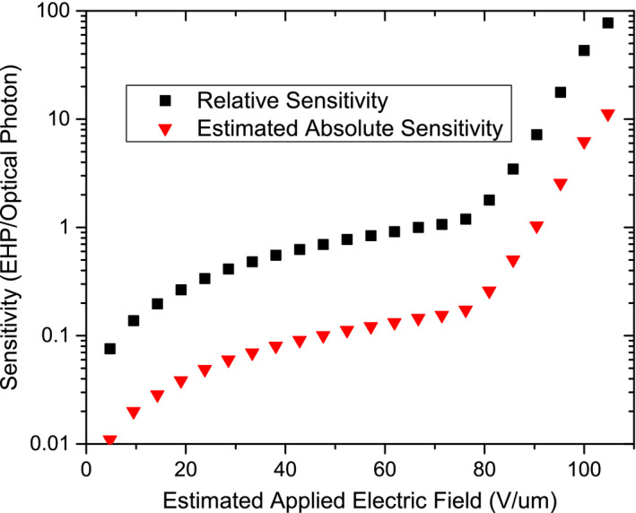
Relative and estimated absolute optical sensitivity of the SHARP‐AMFPI. Relative sensitivity is normalized to E S e = 70 V μm−1. Absolute sensitivity is the effective number of EHPs generated per optical photon incident on the a‐Se. [Color figure can be viewed at wileyonlinelibrary.com]
The linearity of the SHARP‐AMFPI detector with and without g av is shown in Fig. 4 on a log–log scale. Linear fits are shown with the slope at 10 V μm−1 and 90 V μm−1 being 0.245 ± 0.003 and 23.5 ± 0.38 ADU/mR, respectively, with both fittings have r2 values >0.99. The 98‐fold increase in signal is a result of g av = 7 and a 14‐fold increase in the detection efficiency for green light (reduction in geminate recombination) from E Se = 10 V μm−1 to E Se = 90 V μm−1. Saturation of the pixel capacitor from signal and dark current provided the upper limit of the exposure at avalanche fields. Increasing the exposure at low E Se has no merit as it will be shown that the system is limited by secondary quantum noise.
Figure 4.
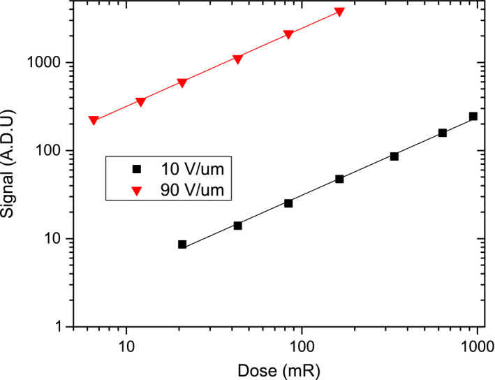
Linearity of the detector. Signal in ADU is shown as a function of exposure to the detector for E S e = 10 and 90 V μm−1 (g av = 7). [Color figure can be viewed at wileyonlinelibrary.com]
Figure 5 shows the measured MTF of the prototype detector for E Se = 10 and 90 V μm−1 (g av = 7). As expected, there is no measurable difference in spatial resolution by the incorporation of g av . The nonavalanche NPS is shown in Fig. 6(a), where the NPS is largely white and dominated by electronic and secondary quantum noise. The electronic noise component of the NPS is 0.015 ADU2 mm2 at all spatial frequencies. X‐ray quantum noise is not seen because at E Se = 10 V μm−1, the quantum efficiency of HARP for green light is only 0.02, preventing x‐ray quantum noise‐limited performance even with an exposure as high as 945 mR. This confirms our predicted values of less than two ehp/x‐ray photon, wherein secondary quantum noise dominates the NPS. When the HV is increased to achieve g av = 7, the dark NPS has increased to 0.17 ADU2 mm2 and remains white as shown in Fig. 6(b). Additionally, correlated x‐ray quantum noise from the scintillator becomes apparent in the NPS.
Figure 5.
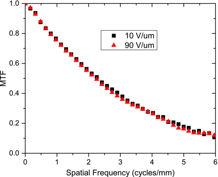
MTF of SHARP‐AMFPI with 150 μm of CsI for E S e = 10 and 90 V μm−1 (g av = 7). [Color figure can be viewed at wileyonlinelibrary.com]
Figure 6.
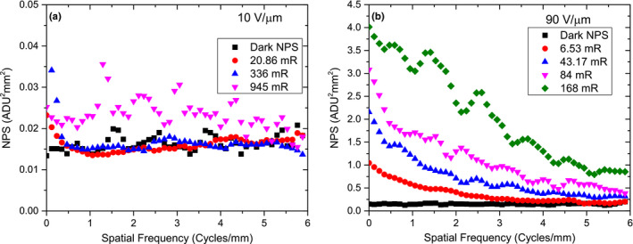
NPS as a function of exposure. (a) NPS for E S e = 10 V μm−1. Electronic noise and secondary quantum noise dominate the NPS. (b) E S e = 90 (g av = 7) quantum noise dominated the NPS. There is an increase in electronic noise at all frequencies with the addition of g av . [Color figure can be viewed at wileyonlinelibrary.com]
To understand the effects of the additional dark current noise, we consider DQE(0) for E Se = 10 V μm−1 (g av = 1, γ = 0.02) and E Se = 90 (g av = 7, γ = 0.28). DQE(0) was calculated by 1/(q*NNPS(0)) where NNPS is the normalized NPS and q is the quanta flux. The DQE(0) measurements were obtained by extrapolating the NNPS to zero frequency to obtain NNPS(0). The measured DQE(0) can be seen in Fig. 7 as a function of exposure. For E Se = 10 V μm−1, DQE(0) < 0.07 for all exposure levels less than 1000 mR. This is due to secondary quantum sink as a result of poor optical quantum efficiency (γ = 0.02). With g av = 7 and a quantum efficiency of 0.28, DQE(0) = 0.52 at 168 mR and decreases to 0.16 at 6.5 mR due to electronic noise. The trend in measured DQE(0) with exposure is in good agreement with theoretical prediction and is discussed in the following section. The fluctuations in the DQE(0) measurement is due to variations in dark current. Normally, the dark current in a‐Se sensors has an exponential decay with time after the HV is turned on.30 Due to the 2 s integration window, the dark current (and dark current noise) during x‐ray exposure may be different from that during the offset frame acquisition.
Figure 7.
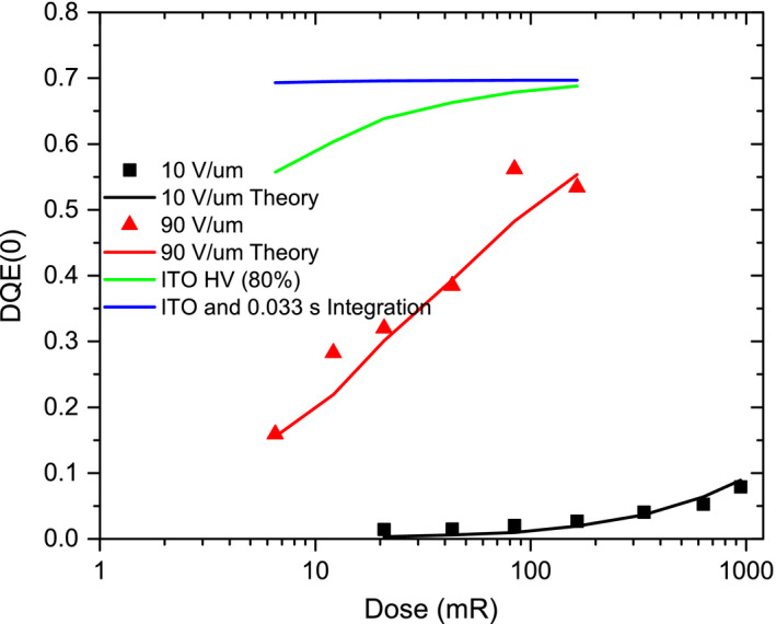
DQE(0) measured and modeled results. Solid dots represent DQE(0) calculated from measured NPS and MTF; solid lines represent modeled DQE(0) using Eq. (3). DQE(0) can be improved with the inclusion of an ITO HV electrode with 80% transmission and a shorter integrating time to reduce dark current noise. [Color figure can be viewed at wileyonlinelibrary.com]
3.B. Cascaded linear modeling for SHARP‐AMFPI
Using the parameters in Table 1 and Eq. (3), we model the DQE(0) and compare it to the measured results shown in Fig. 7. At E Se = 10 V μm−1, the quantum efficiency of HARP for green light is 0.02, which leads to a secondary quantum sink and poor DQE(0), even with an exposure as high as 945 mR. From the NPS measurements in Fig. 6(b), the dark noise increases from 0.018 ADU2 mm2 at E Se = 10 V μm−1 to 0.17 ADU2 mm2 at E Se = 90 V μm−1. As dark current increases at avalanche fields, an additional source of noise must be considered, which is the dark current shot noise.31 With dark current noise included in the S n term of Eq. (3), the variance is given by:
| (4) |
where σ TFT is the electronic noise and σdark is given by:
| (5) |
where Id is the injected dark current, Id‐measured is the measured dark current after avalanche gain, and T is the integrating window of the detector (2 s) between subsequent readouts. Good agreement is seen in Fig. 7 between the modeled and measured DQE(0) for all exposures when the dark current is modeled at 140 pA cm−2.
The DQE(0) results demonstrate the possibility of improvement in DQE for a system that is not already x‐ray quantum noise limited. The relatively large exposures used in this work are a result of two limitations of our prototype system: (a) the low transparency of the HV electrode and (b) the long integration window, which increases the contribution of dark current noise. Removing these limitations is also modeled in Fig. 7. The expected improvement is shown when the transparency of the HV electrode is increased from δ = 0.25 to δ = 0.8. We also model DQE(0) with a shorter integration window (33 ms). This results in lower dark current noise and increases the DQE(0) to its theoretical limit.
3.C. Imaging
X‐ray images obtained with the indirect SHARP‐AMFPI prototype are shown in Fig. 8 with an average detector exposure of 0.76 mR. The g av associated with the E Se used is summarized in Table 2. The difference in image quality between E Se = 15 V μm−1 and E Se = 71 V μm−1 is a result of an increased optical quantum efficiency of HARP for the green light emitted from the CsI. At avalanche fields, there is a substantial improvement in image quality up to E Se = 100 V μm−1, after which no further improvement is noticeable up to E Se of 105 V μm−1. This indicates that the effect of electronic noise is already overcome with g av of ~30. The apparent variation in gray level in the background is due to the thickness nonuniformity of the x‐ray object, which has over a tenth value difference in attenuation from the thinnest to thickest location.
Figure 8.
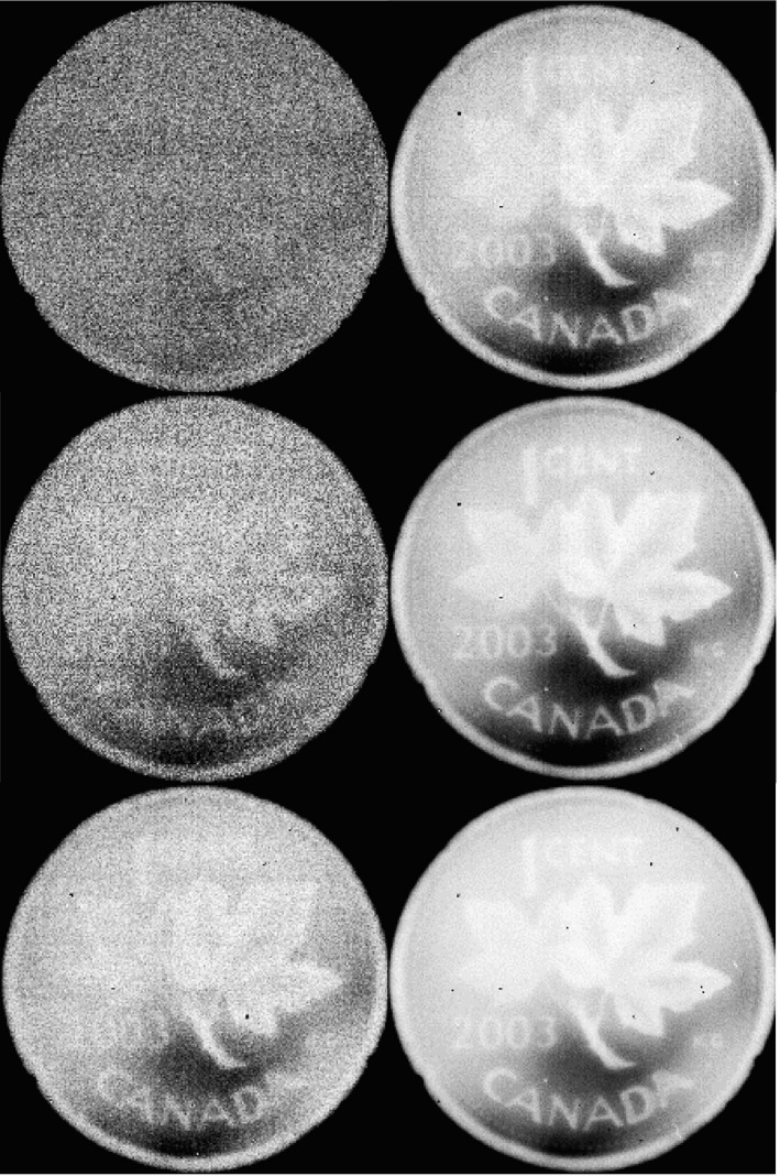
Images of the tails side of a penny with constant 0.76 mR exposure. Left column from top to bottom E S e = 15, 71, and 95 V μm−1. Right column from top to bottom E S e = 95, 100, and 105 V μm−1.
Table 2.
g av and γ used for imaging
| E Se (V μm−1) | 15 | 71 | 90 | 95 | 100 | 105 |
|---|---|---|---|---|---|---|
| g av | 1 | 1.1 | 7.0 | 17.0 | 30.7 | 76.1 |
| γ | 0.02 | 0.15 | 0.28 | 0.31 | 0.33 | 0.38 |
Fig. 9 shows x‐ray images acquired with the average detector exposure reduced from 0.24 mR to 0.02 mR while keeping E Se = 105 V μm−1 constant. These lower exposures are well below that expected for SHARP‐AMFPI in mammography. The detector exposure is estimated as the average value behind the entire x‐ray object. The structural features within the penny can still be seen at exposures as low as 0.02 mR. It is important to note that no image processing has been applied except for an offset subtraction utilizing a dark frame taken immediately before the irradiated frame. As a result, gain variation in the charge amplifiers of the TFT array can be seen in the low‐exposure images as vertical lines.
Figure 9.
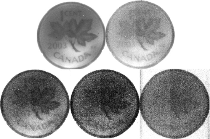
X‐ray images taken at 105 V μm−1 while the detector exposure is reduced. In the top row from left to right, the exposure was 0.24 and 0.11 mR. In the bottom row, the exposure was 0.05, 0.03, and 0.02 mR from left to right.
Figure 10 demonstrates imaging performance with the CIRS BR3D phantom. Images were acquired with E Se = 10, 80, 90, 100 V μm−1. The effects of electronic noise are once again reduced, and image quality continuously improves with E Se through a gain of 30. In addition to improvements in soft tissue contrast, microcalcification beads become clear in the bottom right corner. The cross structure in the images is a result of tiling of the small area CsI scintillator and no gain correction to account for variation in light output.
Figure 10.
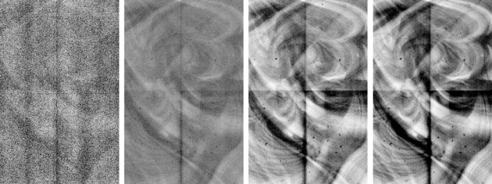
Images of a CIRS BR3D breast‐imaging phantom. From left to right, E S e = 15, 71, 90, and 100 V μm−1. Not only the soft tissue contrast improves but also microcalcification beads become visible in the lower right quadrant. The cross structure is a result of scintillator tiling.
3.D. Future detector improvements
To improve the DQE(0), either the signal must be increased or S n must be decreased. Due to dark current shot noise and the risk of breakdown with increasing E Se , g av should be the lowest value required to overcome S n . To minimize the required g av and E Se , the optical gain parameters in Table 1 should be maximized. The optical coupling efficiency is currently limited by the transparency of the HV electrode (δ = 0.25). Using a highly transparent HV bias electrode, such as Indium Tin Oxide (ITO) with δ > 0.8, the signal can be increased by 320% which will reduce the g av requirements while maintaining the same imaging performance. In turn, this will reduce E Se which will improve detector stability as well as reducing dark current and therefore dark current shot noise. The improvement in DQE(0) with parameters for ITO is shown in Fig. 7. The dark current noise can also be reduced by decreasing the integration time window. For example, a reduction in the integrating window from 2 s to 0.033 s (typical for real time imaging) increases DQE(0) to near the theoretical limit of the scintillator for all exposures considered. This improvement is shown in Fig. 7. For an application, such as CBCT where the readout rate is as fast as 100 fps, the effective noise would be even less.
Further improvement in optical gain can be achieved by increasing the intrinsic optical quantum efficiency of a‐Se (γ) to green light. It has been demonstrated in HARP tube that a layer of tellurium (Te) doped a‐Se can increase the optical sensitivity from γ = 0.38 to γ = 0.72.32 Under avalanche fields, the optical quantum efficiency for light generated from CsI (540 nm) can be increased by nearly a factor of two which will further improve the DQE of SHARP‐AMFPI and allow for measurements at lower exposures. This will also allow the g av and therefore E Se to be reduced, leading to lower dark current and associated noise. An alternative approach is to use a scintillator that emits in the blue wavelength. Currently, the only structured blue scintillator is CsI:Na; however, due to its hydroscopic instabilities, it has not been used in a commercial AMFPI.
Finally, the CsI scintillator must be optimized for specific medical applications in conjunction with the x‐ray energy and required spatial resolution. In addition to the FOS used in this work, CsI has also been deposited onto an Al or a‐C substrates. Lubinsky et al. have shown through pulse height analysis that the choice of substrates can determine the light output and x‐ray photon attenuation as a result of the geometry (e.g., substrate face up or face down).33 The thickness of CsI has been investigated from 150 to 1000 μm. It has been shown that thicker columnar CsI can provide higher quantum efficiency with minimal penalty on the swank factor.26 Increasing the thickness of CsI will also reduce the risk of direct interactions in the a‐Se.
4. Conclusion
We present the first prototype large area flat panel detector with avalanche gain. SHARP‐AMFPI achieved an optical g av = 76 ± 5 at E Se = 105 V μm−1. There is no change in MTF with the inclusion of g av , and spatial resolution is limited by the optical spread in the CsI scintillator. NPS shows the addition of noise associated with dark current which is normally negligible at low field a‐Se AMFPIs. A CLSM for indirect detectors was modified to include dark current noise and fit the measured DQE(0) results. It is shown that with improved optical coupling and a shorter integrating window, DQE(0) limited by the x‐ray quantum efficiency and Swank factor of the scintillator can be achieved. Nonetheless, we demonstrate the ability of avalanche gain to improve the DQE of a system which is not quantum noise limited. Our future work is to improve the transparency of the HV electrode and reduce the effects of ghosting by improvements in the n‐type blocking layer. With further improvement in the HARP structure, frequency‐dependent DQE, ghosting, and lag effects can be analyzed.
Acknowledgments
We gratefully acknowledge financial support from the National Institutes of Health (R01 EB002655 and R01 CA148053). Research on blocking layers was carried out in part at the Center for Functional Nanomaterials, Brookhaven National Laboratory, which is supported by the U.S. Department of Energy, Office of Basic Energy Sciences, under Contract No. DE‐SC0012704. This work has partially been published in as a SPIE medical imaging conference preceding paper entitled “Solid‐state flat panel imager with avalanche amorphous selenium” (2016). This work expands the initial findings to include detailed MTF, NPS, and DQE measurements and modeling.
References
- 1. Rowlands JA, Yorkston J. Flat panel detectors for digital radiography. Handbook Med Imaging. 2000;1:223–328. [Google Scholar]
- 2. Liu X, Shaw CC. a‐Si: H/CsI (Tl) flat‐panel versus computed radiography for chest imaging applications: image quality metrics measurement. Med Phys. 2004;31:98–110. [DOI] [PubMed] [Google Scholar]
- 3. Koch A, Macherel J‐M, Wirth T, et al. Detective quantum efficiency of an x‐ray image intensifier chain as a benchmark for amorphous silicon flat panel detectors. Proc SPIE. 2001;4320:116. [Google Scholar]
- 4. Zhao W, Ji W, Debrie A, Rowlands J. Imaging performance of amorphous selenium based flat‐panel detectors for digital mammography: characterization of a small area prototype detector. Med Phys. 2003;30:254–263. [DOI] [PubMed] [Google Scholar]
- 5. Matsuura N, Zhao W, Huang Z, Rowlands J. Digital radiology using active matrix readout: amplified pixel detector array for fluoroscopy. Med Phys. 1999;26:672–681. [DOI] [PubMed] [Google Scholar]
- 6. Karim KS, Vygranenko YK, Avila‐Munoz A, et al. Active pixel image sensor for large‐area medical imaging. Proc SPIE. 2003;5030:38–47. [Google Scholar]
- 7. El‐Mohri Y, Antonuk LE, Koniczek M, et al. Active pixel imagers incorporating pixel‐level amplifiers based on polycrystalline‐silicon thin‐film transistors. Med Phys. 2009;36:3340–3355. [DOI] [PMC free article] [PubMed] [Google Scholar]
- 8. Zhao C, Kanicki J. Amorphous In–Ga–Zn–O thin‐film transistor active pixel sensor x‐ray imager for digital breast tomosynthesis. Med Phys. 2014;41:091902. [DOI] [PubMed] [Google Scholar]
- 9. Zhao W, Li D, Reznik A, et al. Indirect flat‐panel detector with avalanche gain: fundamental feasibility investigation for SHARP‐AMFPI (scintillator HARP active matrix flat panel imager). Med Phys. 2005;32:2954–2966. [DOI] [PubMed] [Google Scholar]
- 10. Reznik A, Zhao W, Ohkawa Y, Tanioka K, Rowlands J. Applications of avalanche multiplication in amorphous selenium to flat panel detectors for medical applications. J Mater Sci: Mater Electron. 2009;20:63–67. [Google Scholar]
- 11. Wronski M, Zhao W, Tanioka K, Decrescenzo G, Rowlands JA. Scintillator high‐gain avalanche rushing photoconductor active‐matrix flat panel imager: zero‐spatial frequency x‐ray imaging properties of the solid‐state SHARP sensor structure. Med Phys. 2012;39:7102–7109. [DOI] [PMC free article] [PubMed] [Google Scholar]
- 12. Juška G, Arlauskas K. Impact ionization and mobilities of charge carriers at high electric fields in amorphous selenium. Phys Status Solidi. 1980;59:389–393. [Google Scholar]
- 13. Tsuji K, Takasaki Y, Hirai T, Yamazaki J, Tanioka K. Avalanche phenomenon in amorphous selenium. Optoelectron‐Devices Technol. 1994;9:367–378. [Google Scholar]
- 14. Reznik A, Baranovskii S, Rubel O, et al. Avalanche multiplication in amorphous selenium and its utilization in imaging. J Non‐Cryst Solids. 2008;354:2691–2696. [Google Scholar]
- 15. Stephens R. Relaxation effects in glassy selenium. J Non‐Cryst Solids. 1976;20:75–81. [Google Scholar]
- 16. Scheuermann JR, Miranda Y, Liu H, Zhao W. Charge transport model in solid‐state avalanche amorphous selenium and defect suppression design. J Appl Phys. 2016;119:024508. [Google Scholar]
- 17. Tanioka K, Shidara K, Harai T. Highly sensitive camera tube using avalanche multiplication in an amorphous selenium photoconductive target. In: SPIE/IS&T 1992 Symposium on Electronic Imaging: Science and Technology; 1992:2–12.
- 18. Tanioka K. High‐gain avalanche rushing amorphous photoconductor (HARP) detector. Nucl Instrum Methods Phys Res, Sect A. 2009;608:S15–S17. [Google Scholar]
- 19. Bubon O, Decrescenzo G, Zhao W, et al. Electroded avalanche amorphous selenium (a‐Se) photosensor. Curr Appl Phys. 2012;12:983–988. [DOI] [PMC free article] [PubMed] [Google Scholar]
- 20. Takiguchi Y, Maruyama H, Kosugi M, et al. CMOS imager hybridized to an avalanche multiplied film. IEEE Trans Electron Devices. 1997;44:1783–1788. [Google Scholar]
- 21. Scheuermann JR, Goldan AH, Tousignant O, Léveillé S, Zhao W. Low dose digital X‐ray imaging with avalanche amorphous selenium. Proc SPIE. 2015;9412:94120E. [DOI] [PMC free article] [PubMed] [Google Scholar]
- 22. Scheuermann JR, Howansky A, Goldan AH, et al. Solid‐state flat panel imager with avalanche amorphous selenium. Proc SPIE. 2016;9783:978317. [Google Scholar]
- 23. Zhao B, Zhao W. Temporal performance of amorphous selenium mammography detectors. Med Phys. 2005;32:128–136. [DOI] [PubMed] [Google Scholar]
- 24. Fujita H, Tsai D‐Y, Itoh T, et al. A simple method for determining the modulation transfer function in digital radiography. IEEE Trans Med Imaging. 1992;11:34–39. [DOI] [PubMed] [Google Scholar]
- 25. Zhao B, Zhao W. Imaging performance of an amorphous selenium digital mammography detector in a breast tomosynthesis system. Med Phys. 2008;35:1978–1987. [DOI] [PMC free article] [PubMed] [Google Scholar]
- 26. Howansky A, Peng B, Lubinsky AR, Zhao W. Deriving depth‐dependent light escape efficiency and optical Swank factor from measured pulse height spectra of scintillators. Med Phys. 2017;44:847–860. [DOI] [PMC free article] [PubMed] [Google Scholar]
- 27. Cunningham IA, Westmore M, Fenster A. A spatial‐frequency dependent quantum accounting diagram and detective quantum efficiency model of signal and noise propagation in cascaded imaging systems. Med Phys. 1994;21:417–427. [DOI] [PubMed] [Google Scholar]
- 28. Pai DM, Enck RC. Onsager mechanism of photogeneration in amorphous selenium. Phys Rev B. 1975;11:5163–5174. [Google Scholar]
- 29. Scheuermann JR, Goldan AH, Tousignant O, Léveillé S, Zhao W. Development of solid‐state avalanche amorphous selenium for medical imaging. Med Phys. 2015;42:1223–1226. [DOI] [PMC free article] [PubMed] [Google Scholar]
- 30. Frey JB, Belev G, Tousignant O, Mani H, Laperriere L, Kasap SO. Dark current in multilayer stabilized amorphous selenium based photoconductive x‐ray detectors. J Appl Phys. 2012;112:014502. [Google Scholar]
- 31. Weisfield RL, Bennett NR. Electronic noise analysis of a 127‐μm pixel TFT/photodiode array. Proc SPIE. 2001;4320:209–218. [Google Scholar]
- 32. Park W‐D, Tanioka K. Avalanche characteristics of the Te‐doped amorphous se photoconductive target for a complementary metal–oxide–semiconductor image sensor. Jpn J Appl Phys. 2006;45:L307. [Google Scholar]
- 33. Lubinsky A, Zhao W, Ristic G, Rowlands J. Screen optics effects on detective quantum efficiency in digital radiography: zero‐frequency effects. Med Phys. 2006;33:1499–1509. [DOI] [PubMed] [Google Scholar]


