Abstract
Our latest developments in miniaturizing 3D printed microfluidics [Gong et al., Lab Chip, 2016, 16, 2450; Gong et al., Lab Chip, 2017, 17, 2899] offer the opportunity to fabricate highly integrated chips that measure only a few mm on a side. For such small chips, an interconnection method is needed to provide the necessary world-to-chip reagent and pneumatic connections. In this paper we introduce Simple Integrated Microgaskets (SIMs) and Controlled-Compression Integrated Microgaskets (CCIMs) to connect a small device chip to a larger interface chip that implements world-to-chip connections. SIMs or CCIMs are directly 3D printed as part of the device chip, and therefore no additional materials or components are required to make the connection to the larger 3D printed interface chip. We demonstrate 121 chip-to-chip interconnections in an 11×11 array for both SIMs and CCIMs with an areal density of 53 interconnections/mm2, and show that they withstand fluid pressures of 50 psi. We further demonstrate their reusability by testing devices 100 times without seal failure. Scaling experiments show that 20×20 interconnection arrays are feasible, and that CCIM areal density can be increased to 88 interconnections/mm2. We then show the utility of spatially distributed discrete CCIMs by using an interconnection chip with 28 chip-to-world interconnects to test 45 3D printed valves in a 9 × 5 array. Each valve is only 300 µm in diameter (the smallest yet reported for 3D printed valves). Every row of 5 valves is tested to at least 10,000 actuations, with one row tested to 1,000,000 actuations. In all cases there is no sign of valve failure, and the CCIM interconnections prove an effective means of using a single interface chip to test a series of valve array chips.
Graphical abstract
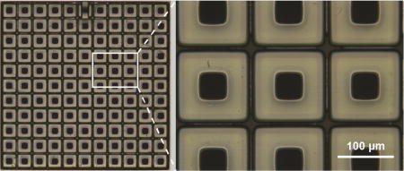
We develop a new high-density, reversible, chip-to-chip interconnection method for hundreds of interconnects that is 3D printed as part of the connecting chips.
1 Introduction
Our recent work has focused on developing materials, tooling, and methods to enable 3D printing to successfully fabricate microfluidic devices with features in the truly microfluidic, as opposed to millifluidic, regime1 for both passive and active components.2–4 For example, we recently (2017) developed a custom Digital Light Processing stereolithographic (DLP-SLA) 3D printer and associated photopolymerizable resin with which we demonstrated reliable 3D printing of flow channels with cross sections as small as 18 µm × 20 µm.4 Previously (2016), we demonstrated that our earlier custom resin and commercial 3D printer work (60 µm × 108 µm cross section flow channels)2 enabled dense 3D layout of devices that included integrated valves and pumps.3 We are now applying our new 3D printer and resin to realize even smaller valves and pumps, in which we are seeing a 30× reduction in valve volume compared to our 2016 work. Our expectation is that fully using all 3 spatial dimensions for component layout in conjunction with our new materials and methods will routinely result in 3D printed microfluidic devices with volumes on the order of 10 mm3 or less. With such small size (only a few mm on a side), we anticipate that many devices (tens to ~100) can be simultaneously printed in a single one hour 3D print run, thereby launching the possibility of using 3D printing for not only device prototyping, but also device manufacturing. This would have a profound impact on the microfluidics development process by eliminating the current separation between prototyping and manufacturing, which typically rely on entirely different processes and materials resulting in two independent and expensive development cycles, and instead consolidate them to use the same tools and materials.
A critical aspect of realizing this vision is being able to make 10’s to possibly 100’s of interconnections to such small chips in order to provide the necessary fluid and pneumatic i/o’s. However, current world-to-chip interconnect methods achieve an areal density of at best 1/mm2,5–15 and are therefore unsuitable for this purpose. In this paper we propose that the world-to-chip interface be delegated to a separate, larger interface chip that in turn is connected through a new high density chip-to-chip interconnect to a much smaller device chip. The interface chip would be re-usable with a sequence of disposable small device chips, and could itself be 3D printed. The interface chip could either be designed to be specific for a particular type of device chip, or it could be implemented as a more universal interface for a variety of device chips. In either case it could implement one of a number of world-to-chip interfaces (see for example a recent review in Ref. 16 that has some possible interfaces), together with the new high density interconnects we report in this paper in order to form a bridge between lab-scale support equipment and small-volume, highly integrated 3D printed chips, which in turn lend themselves to mass manufacturing with 3D printing.
The chip-to-chip interconnect method we develop in this paper is designed to meet the following criteria: (1) support large numbers of interconnects at (2) high density (10’s/mm2) while (3) withstanding pneumatic and fluid pressures typical for 3D printed microfluidic valves and pumps (at least 20 psi) and that are (4) reusable and (5) easy to align and connect. We show that these objectives can be achieved with a Simple Integrated Microgasket (SIM) that is directly 3D printed as part of a device chip. Moreover, we show that a more refined Controlled-Compression Integrated Microgasket (CCIM) can be directly integrated with no increase in fabrication time or complexity because of the ease of 3D printing. In both cases we demonstrate 11×11 arrays of interconnects in an area of 1.5×1.5 mm2 (53 interconnects/mm2) that withstand 100 separations and re-connections with no degradation in performance for an applied pressure up to 50 psi. We then investigate the scaling properties of CCIMs by demonstrating a 20×20 array of interconnects in an area of 3.0×3.0 mm2, and by showing that the areal density can be increased to 88 interconnects/mm2. In short, using our approach, large numbers of high density chip-to-chip interconnects can be readily formed as part of a 3D printed microfluidic device (including alignment structures) with no requirement for additional materials or separately fabricated parts, thereby facilitating the vision outlined above.17
Finally, to illustrate the utility of CCIM interconnects to accommodate a large number of world-to-chip connections, we use a spatially distributed set of discrete CCIMs as part of testing our new, miniaturized 3D printed pneumatic membrane valves that are only 300 µm in diameter. We demonstrate 28 world-to-chip connections in an interface chip with 28 chip-to-chip CCIMs to do lifetime testing of 45 valves arranged in a 9 × 5 array in a device chip.
2 Materials and methods
2.1 3D printer and materials
The 3D printer used in this work is the custom 3D printer we describe in Ref. 4 with a 385 nm LED light source and a pixel pitch of 7.6 µm in the plane of the projected image. The photopolymerizable resin is the poly(ethylene glycol) diacrylate (PEGDA, MW258) resin with 1% (w/w) phenylbis(2,4,6-trimethylbenzoyl)phosphine oxide (Irgacure 819) photoinitiator and 2% (w/w) 2-nitrophenyl phenyl sulfide (NPS) UV absorber described in the same reference, which also details the suppliers we use for these materials.
2.2 3D printing
3D prints are fabricated on diced and silanized glass slides.4 Each slide is prepared by cleaning with acetone and isopropyl alcohol (IPA), followed by immersion in 10% 3-(trimethoxysilyl) propyl methacrylate in toluene for 2 hours. After silane deposition slides are kept in toluene until use. The build layer thickness is 10 µm, and each build layer is exposed with a measured optical irradiance of 21.2 mW cm−2 in the image plane. Unless otherwise noted, the layer exposure time is 600 ms. After printing, unpolymerized resin in interior regions is gently flushed with IPA, followed by device UV curing in an inexpensive consumer UV nail curer (54 Watt Professional UV Nail Dryer, Royal Nails) that emits a broad spectrum.4
2.3 Surface roughness measurement
Surface roughness measurements are made with a 3D printed rectangular block comprised of 4 adjacent equal-area regions, each of which has a different layer exposure time (600, 800, 1000, and 1200 ms). After fabrication, the surface roughness is measured in three different ~0.1 mm2 areas in each exposure region and the average root-mean-square (RMS) roughness is calculated based on these measurements. Measurements are made with a Zeta-20 3D optical profiler (Zeta Instruments, San Jose, California) using a 10× objective lens.
2.4 Pressure and reusability measurements
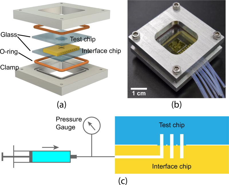
For pressure testing, an interface chip and test chip are aligned and clamped together with a custom aluminum clamp as shown in Figs. 1(a) and 1(b). The test chip and interface chip are first fitted together using the matching 3D printed alignment features on each chip. These are then placed between machined aluminum pieces that have central cut-outs to facilitate optical access to the test and interface chips. O-rings are used on the interior lips of the aluminum pieces to avoid direct contact between the metal and glass slides on which the chips are 3D printed. The only tool required is a hex key which is used to gently (using two fingers) torque the four screws that hold the aluminum pieces together.
Fig. 1.
(a) Clamping mechanism for interface and test chips. (b) Photo of clamped interface and test chips ready for pressure testing. (c) Schematic illustration of pressure test set up. Syringe pump is connected sequentially to individual tubes to pressure test each associated interconnection port microgasket (see text for details).
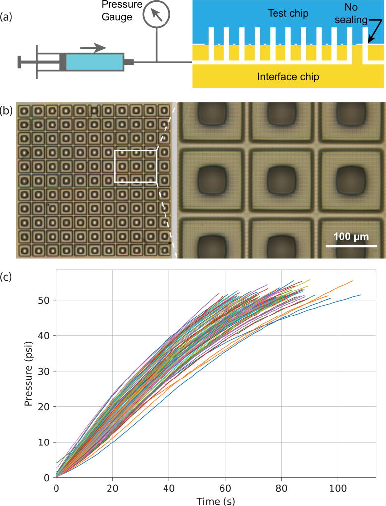
To test the performance of a single microgasket, a syringe pump is used to pressurize a given interconnect through its specific chip-to-world interface as shown in Fig. 1(c). Pressure is monitored with an electronic pressure transducer as the syringe pump pushes deionized (DI) water into the test chip at a flow rate of 50 µL/min. Any compromise in the seal integrity of the microgasket manifests itself as a drop in pressure, which is readily measured with the pressure transducer.
The same basic process is used to test the 11×11 interconnection arrays in Sections 3.2 and 3.3 except that a parallel technique is applied in which 120 (out of 121) interconnects on the interface chip are routed to a single PTFE tube such that they can all be pressurized simultaneously using a syringe pump. (See Ref. 3 for details on PTFE tubing and our attachment method.) If there is any leakage between the microgaskets and the interface chip, the pressure is released through the 121st interconnect which is deliberately fabricated with an incomplete microgasket, and which is connected to a second PTFE tube. Microgasket leakage therefore manifests itself as not only a drop in pressure, but also the appearance of DI water in the second PTFE tube. To test the reusability of the interconnections between the interface and test chips, the clamp mechanism and interface and test chips for the 11×11 interconnection arrays in Sections 3.2 and 3.3 are disassembled after a pressure test, followed by re-assembly and another pressure test. This is repeated 100 times.
3 Results and discussion
3.1 Concept
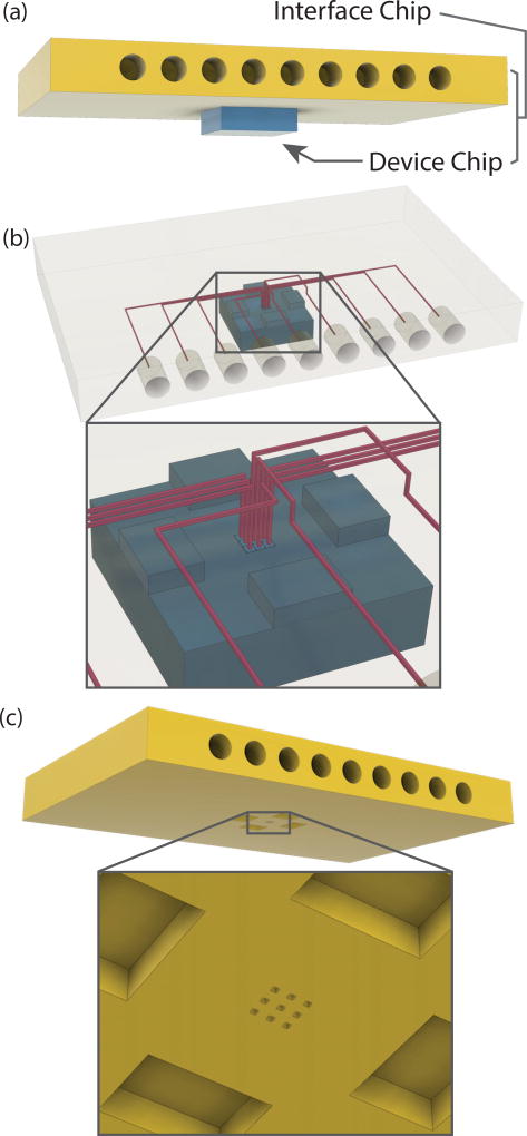
The basic idea of using an interface chip to act as a chip-to-world intermediary for a small device chip is shown in Fig. 2(a), where, as an example, 9 cylindrical recesses for PTFE tubing are shown as the world interface on one edge of the chip, and on the bottom of the chip is a small 3×3 array of vertical channels (Figs. 2(b) and (c)) that interface with a matching set of channels on the device chip.
Fig. 2.
(a) Schematic illustration of a 3.4×3.4×1 mm3 device chip connected to an interface chip (clamping mechanism not shown). The interface chip supplies a world-to-chip interface with an array of cylindrical recesses into which PTFE tubing is epoxied. (b) Schematic illustration of the interior of the interface chip showing how channels are routed from the cylindrical recesses to an array of interconnects on the device chip. Alignment blocks on the top of the device chip are also visible. (c) Underside of interface chip. Close-up shows that interconnects consist of an array of flow channels that terminate on the flat bottom surface of the chip, and that the device chip alignment blocks fit into recesses on the interface chip.
Alignment of the two chips is achieved with four rectangular recesses in the bottom of the interface chip (Fig. 2(c)) into which fit matching rectangular blocks on the device chip (Fig. 2(b)). We typically design the width of the rectangular blocks to be 2 pixels wider than the recesses to account for slight material shrinkage and to ensure a snug fit. With this approach we generally see an alignment accuracy of approximately one pixel between the vertical channels on the interface and device chips. Also, the recesses are designed to be deeper than the height of the blocks so that the lower surface of the interface chip contacts the upper surface of the device chip when they are clamped together as in Fig. 1.
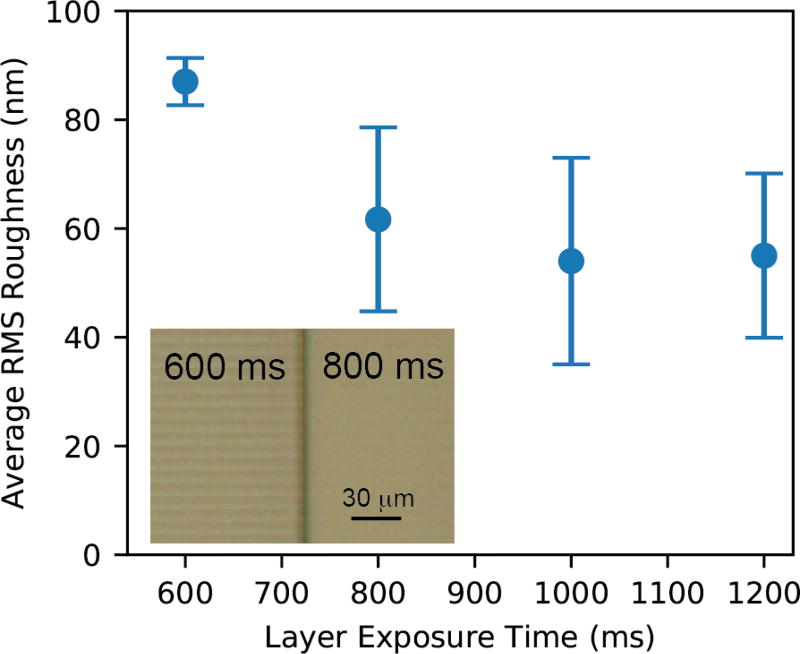
Fortunately, horizontal surfaces as fabricated in our custom 3D printer are exceptionally smooth. As seen in Fig. 3, the average RMS surface roughness is 87 nm for a layer exposure time of 600 ms. The roughness is primarily due to slightly depressed pixel edges as seen in the inset Zeta-20 microscope image as a barely visible square pattern of lines. This in turn is presumably due to the slightly lower optical dose along the projected pixel edges compared to the interior of each pixel region. Lower dose means less crosslinking in the polymer matrix such that some of the material may be marginally soluble in the isopropyl alcohol rinse that follows 3D printing. Note that as the layer dose increases, the average RMS roughness decreases until it asymptotes to ~55 nm. Compared to the 600 ms layer exposure time, an increase of 33% to 800 ms results in a noticeably decreased square pattern in the inset image, indicating that more of the photopolymerized material at the pixel edges remains as part of the final print after rinsing. Since the RMS roughness is already very small at 600 ms exposure time, we choose to use this exposure in our tests since longer exposure times involve a tradeoff with the minimum achievable channel height.2–4 We believe that the smooth as-printed horizontal surfaces in conjunction with the modest flexibility of our 3D printed material (Young’s Modulus ~7–8 MPa)4 are the fundamental reasons that our high density interconnects work so well.
Fig. 3.
Measured average surface roughness as a function of layer exposure time. The error bars indicate the standard deviation of the three measurements for each exposure time that are described in Sect. 2.3. Inset: microscope photo of device with adjacent regions having 600 and 800 ms layer exposure times. Faint pixelation is more observable for the former than the latter.
3.2 Simple integrated microgasket (SIM) approach
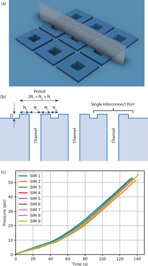
A simple approach to forming leak-free interconnects is shown in Fig. 4(a) in which a square microgasket is printed around each vertical channel on the device chip. We find that tall microgaskets (D = 100 µm) typically do not survive more than one clamping event in that many of the microgaskets become crushed. However, if the microgasket is only 10 µm thick (i.e., one build layer), it survives a clamping event without noticeable damage.
Fig. 4.
SIM design. (a) Integrated square microgaskets printed around each vertical channel on the top surface of a device chip. The top surface is in the XY plane with the Z direction being out of the plane. (b) Schematic illustration of the cross section of the vertical plane indicated in (a). The microgaskets have height D above the surrounding planar surface of the chip. (c) Pressure as a function of time for the test set up in Fig. 1(c) using the device and interface chips in Fig. 2 for each of the 9 chip-to-chip interconnects.
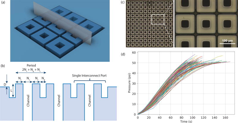
A schematic cross sectional profile of the microgaskets and channels is shown in Fig. 4(b). A channel is Nc pixels wide surrounded by a microgasket with a Ns pixel wide sealing surface and a gap of Ng pixels with the next microgasket. The period is
| (1) |
pixels, with a physical period of 7.6 µm times Nper.
We fabricated the interface and device chips shown in Fig. 2 (the latter with SIM microgaskets having a microgasket height of D = 10 µm) with an interconnection period of 24 pixels (182.4 µm) in both X and Y for an areal density of 30 interconnects/mm2 (see Table 1 for geometry details). Pressure test results for each of the 9 interconnects are shown in Fig. 4(c), in which the pressure that builds up during syringe pump operation is shown as a function of time for each of the tests. In all cases, the pressure rises monotonically to ~50 psi, at which point the test is terminated because leaks develop in the testing setup itself (i.e., the syringe gasket and various PTFE tube-to-tube connections). For each test, there is no evidence of leakage in the corresponding interconnect port, indicating that the ports maintain their integrity to at least 50 psi.
Table 1.
Experimentally tested interconnect array sizes and periods.
| Leak-free? | Array | Nc | Ns | Ng | Period (pixels) | Period (µm) | Density (mm2) |
|---|---|---|---|---|---|---|---|
| Y | 3×3 | 6 | 6 | 6 | 24 | 182.4 | 30.0 |
|
| |||||||
| Y | 11×11 | 6 | 5 | 4 | 20 | 152 | 43.3 |
|
| |||||||
| Y | 11×11 | 6 | 5 | 2 | 18 | 136.8 | 53.4 |
| 20×20 | |||||||
|
| |||||||
| Y | 11×11 | 6 | 4 | 1 | 15 | 114 | 76.9 |
|
| |||||||
| Y | 11×11 | 6 | 3 | 2 | 14 | 106.4 | 88.3 |
|
| |||||||
| N | 11×11 | 6 | 3 | 1 | 13 | 98.8 | 102.4 |
|
| |||||||
| N | 11×11 | 6 | 2 | 2 | 12 | 91.2 | 120.2 |
|
| |||||||
| N | 11×11 | 6 | 2 | 1 | 11 | 83.6 | 143.1 |
To test a larger number of interconnects at higher density, we designed an 11×11 array of interconnects as shown in Fig. 5 with a period of 18 pixels (136.8 µm) in both X and Y for an areal density of 53 interconnects/mm2 (third row in Table 1), and a microgasket height of D = 10 µm. Note that the fidelity and uniformity of the microgasket and vertical channel features is excellent, which is typical for the many SIM and CCIM devices we have 3D printed over several months.
Fig. 5.
(a) 11 × 11 interconnect array test set up. (b) Composite image from four Zeta-20 microscope images of fabricated 11×11 array of SIMs. Close up shows details of SIMs, including slight pixelation of the sealing surface. (c) Pressure as a function of time for the test set up in (a) repeated 100 times.
The results of pressure testing for 100 repeated tests are shown in Fig. 5(c). The pressure that builds up during syringe pump operation is shown as a function of time for each of the runs. In all cases, there is no evidence of leakage in the interconnect ports, indicating that the ports maintain their integrity to at least 50 psi. As before, testing is terminated at 50 psi due to leaks in the testing apparatus.
3.3 Controlled-compression integrated microgasket (CCIM) approach
After 100 pressure tests, the planar surface of the interface chip for the SIM case begins to show slight signs of wear when observed in the Zeta-20. We therefore investigated an alternate microgasket design in which the compression of the microgasket is controlled by the geometry of the design (CCIM), as shown in Figs. 6(a) and (b). The design features square microgaskets in a recessed region. The microgasket height, L, is 100 µm and the recess is 90 µm such that D = 10 µm as for the SIM case. When the CCIMs on a device chip are clamped to an interface chip, the microgaskets compress 10 µm (i.e., 10% of their height) because the planar surface of the interface chip lands on the surrounding planar surface of the device chip, preventing further compression of the microgaskets. This therefore limits the amount of force the microgaskets exert on the corresponding planar surface of the interface chip.
Fig. 6.
CCIM design. (a) Integrated microgaskets printed around each vertical channel in a square recess. (b) Schematic illustration of the cross section of the vertical plane in (a). The microgaskets have height D above the surrounding planar surface of the chip. (c) Composite image from four Zeta-20 microscope images of fabricated 11×11 array of CCIMs. Close up shows details of CCIMs. (d) Pressure as a function of time for the test set up in Fig. 5(a) repeated 100 times.
A fabricated 11×11 CCIM device chip is shown in Fig. 6(c) with the same XY dimensions as the SIM device chip in Fig. 4(c) (i.e., third row in Table 1). Corresponding pressure tests are shown in Fig. 6(d). Similar to the SIM device results, the CCIM tests show no evidence of leakage in the interconnect ports. Microscope observation of the interface chip interconnect surface shows less evidence of wear than for the SIM interconnect case. We have therefore focused on the CCIM design as our standard high density interconnect method. Note that with 3D printing there is no additional time, cost, or process complexity to fabricate the more complicated CCIM design compared to the SIM design. Nonetheless, the SIM design appears to be suitable for situations in which relatively few repeated sealings are required.
3.4 Scaling
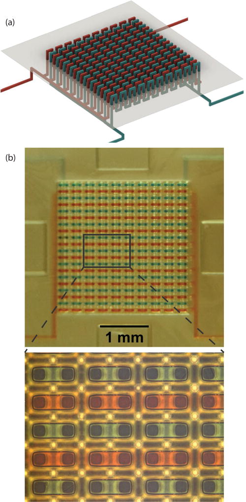
We investigated the potential to scale the CCIM design of Sect. 3.3 to larger numbers of interconnects. Keeping the same XY dimensions, we find that arrays of 20×20 interconnects are easily achieved. An example is shown in Fig. 7 in which two independent microfluidic channels are vertically routed up and down across the chip-to-chip interface in an area of only 3×3 mm2. One channel is filled with red food coloring and the other with blue food coloring. The close-up microscope image in Fig. 7(b) is focused on the highest horizontal channels in the device chip, and shows the very good fidelity and uniformity of the channels and interconnects.
Fig. 7.
(a) Schematic illustration of geometry to test 400 CCIM interconnects in a 20×20 array using two independent sets of flow channels (red and blue) that cross up and down between the chips. The plane shows the separation between device (upper) and interface (lower) chips. (b) Photograph of assembled device and interface chips. The two separate flow channels are filled with water containing red and blue food coloring. (Close-up) Microscope image of flow channels.
Continuing to scale up the array size with the same CCIM XY dimensions, we found limitations when we reached 1,024 interconnects (32×32 array). A small amount of differential shrinkage between the interface and device chips caused the outer interconnection ports to have enough misalignment that they would not seal. This can be overcome by increasing the size of the microgaskets and therefore the period of the interconnects. However, we chose not to pursue this approach because of the concomitant decrease in interconnection density.
Instead, we evaluated whether the interconnect density can be increased for 11×11 arrays, the results of which are summarized in Table 1. For a vertical channel width, Nc, of 6 pixels, we found that the seal width, Ns, could be decreased from 5 pixels to 3 pixels, such that, keeping the gap width, Ng, the same at 2 pixels, the period is reduced to 14 pixels (106.4 µm) for an areal density of 88 interconnects/mm2. With these dimensions, the interconnects still withstand an internal fluid pressure of 50 psi.
Decreasing the period any further results in interconnect arrays that do not fully seal. This appears to be due to shrinkage of the interface chip port geometry which is exacerbated by the relatively smaller volume of polymerized material that results from the high vertical channel density.
4 Demonstration: valve testing
In our group we now use CCIM interconnects for nearly all of our 3D printed microfluidic device development efforts because of how convenient it is to separate the chip-to-world interface from the actual device chip. As an example, consider the miniaturization of pneumatic membrane valves enabled by our custom 3D printer and NPS resin. We originally demonstrated membrane valves with a PEGDA material in 2014 using a conventional cleanroom fabrication process.18 These valves had a diameter of 700 µm. We reported our first 3D printed membrane valves in 2015 using a B9 Creator 3D printer with a custom PEGDA resin.19 Because of the limited resolution (50 µm pixel pitch) of the B9 Creator, the minimum demonstrated valve diameter was 2 mm. In 2016 we showed 1.08 mm diameter valves with a similar custom resin and an Asiga Pico Plus 3D printer having a 27 µm pixel pitch.3 Since our custom 3D printer has a 7.6 µm pixel pitch, this suggests that it should be able to fabricate 300 µm diameter valves (i.e., 1.08 mm × (7.6 µm/27 µm)), which we demonstrate in this section.
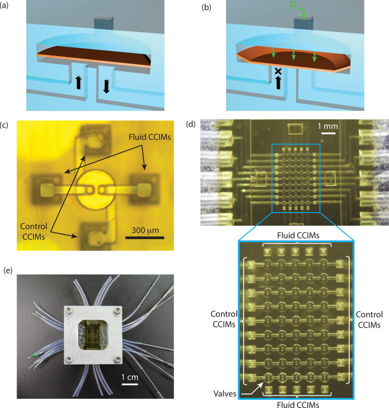
Figures 8(a) and (b) show the geometry of a 3D printed membrane valve. Fig. 8(c) shows a 300 µm diameter 3D printed valve with its two fluid channels and two control channels connected to CCIMs such that the PTFE tubing chip-to-world connections are made with a separate interface chip. The valve membrane consists of two stacked 5 µm layers, each exposed for 300 ms, and fluid and control chambers (i.e., the regions below and above the membrane in Fig. 8(a)) that are 20 µm and 30 µm tall, respectively. A control pressure of 9 psi works well to close such valves.
Fig. 8.
Schematic diagrams of 3D printed pneumatically actuated membrane valve in (a) open and (b) closed states. (after Ref. 3). (c) Single 300 µm diameter valve with fluid and control channels connected to individual CCIMs. (d) (upper) Microscope image of 45-valve arrayx chip assembled with corresponding interface chip in clamping fixture as shown in (e). (d) (lower) Close-up of 45-valve array with each row of valves having their control ports connected in series to a pair of CCIMs, and each column of valves having their fluid ports connected in series to a pair of CCIMs. Each valve is 300 µm in diameter.
To test the valves we constructed an array of 45 valves arranged in 9 rows and 5 columns as shown in Fig. 8(d). The control chambers of each row of valves are connected in series to a pair of CCIMs, and the fluid chambers of each column of valves are likewise connected in series to a pair of CCIMs such that there are a total of 28 CCIMs. The CCIMs are arranged around the periphery of the valve array, rather than concentrated in a small area as in Sect. 3. An interface chip connects these CCIMs through fluid channels to a set of 28 PTFE tubes as shown in Fig. 8(e), in which the interface and valve array chips are clamped together. The photograph in Fig. 8(d) is taken through the glass substrate of the valve array chip and focused on the valve array, which means the CCIMs and channels in the interface chip are somewhat out of focus since they are outside the depth of focus of the camera’s imaging system.
After 3D printing, unpolymerized resin is flushed from the channels and the fluid and control chambers of the valves by first clamping together the valve array and interface chips, after which vacuum and IPA is applied to a pair of tubes connected to one of the rows or columns of valves. This is repeated for each row and each column of valves until all of the unpolymerized resin is flushed. (Note that flushing unpolymerized resin from a valve’s control chamber necessitates two connections to the control chamber.) After thorough flushing, the valve array chip is separated from the interface chip and optically cured.
To test the valves, the valve array and interface chips are again clamped with the aluminum fixture. One set of PTFE tubes connected to the control chambers is blocked by inserting small pieces of wire into their ends (the left set of tubes in Fig. 8(e)), while the other control chamber PTFE tubes are connected to their own solenoid valves and a pressure source. This allows each row of valves to be actuated with a single solenoid valve connected to a manifold pressurized at 9 psi. A water source suspended ~30 cm above the valve chip (and therefore pressurized by gravity) is connected to each column of valves through the top PTFE tubes, and flow is observed through the bottom PTFE tubes as a function of whether any row of valves is actuated or not. The top 8 rows of valves were actuated 10,000 times and the bottom row was actuated 1,000,000 times, after which all of the valves still function normally. A video of valve operation after this lifetime testing is shown in Video S1†, where they are actuated with a 50 ms scrolling cycle.
Finally, we note that we have re-used the interface chip and its 28 world-to-chip connections to test a variety of 3D printed test chips containing different sized valves, displacement chambers,3 and pumps. Interconnect chip re-use has proven to be an extremely convenient laboratory benefit of CCIMs.
5 Conclusions
We have shown that high density chip-to-chip interconnections are feasible between two 3D printed chips using only 3D printed structures on the chips themselves, i.e., no additional materials or parts are needed to effect a seal between the chips other than a mechanism to press the chips together. We have also shown that passive integrated alignment structures are sufficient to attain the necessary alignment accuracy between the two chips. We have introduced both SIM and CCIM geometries for integrated microgaskets, and have shown that both approaches withstand internal fluid pressures up to at least 50 psi in 11×11 arrays of interconnections with an areal density of 53 interconnects/mm2, and can do so with no degradation in performance for 100 repeated tests. CCIM interconnections have been demonstrated for up to 400 interconnects (20×20), and up to an areal density of 88 interconnects/mm2. SIM and CCIM interconnections therefore fulfill the 5 chip-to-chip interconnect criteria set forth in the Introduction, namely, (1) support large numbers of interconnects at (2) high density while (3) withstanding pneumatic and fluid pressures typical for 3D printed microfluidic valves and pumps and that are (4) reusable and (5) easy to align and connect.
In addition, we have shown an application of spatially distributed CCIMs in which they are used to simplify testing a 45 valve array with 28 world-to-chip interconnects, in the course of which we have demonstrated the smallest 3D printed valves to date (300 µm diameter).
In this paper we have focused on connecting a single device chip to an interface chip. We should note that it is also possible to connect multiple device chips to the same interface chip and either drive them all in parallel, or create some combination of parallel and independent fluid and pneumatic connections. As a further observation, device chips could also be stacked vertically, one underneath another, with high density interconnections on both their top and bottom surfaces to chain them together. Finally, the 3D printed interface chip need not be only a passive device to route world connections to device chips; it could also incorporate active functions.
Supplementary Material
Acknowledgments
We are grateful to the National Institutes of Health (R01EB006124 and R15GM123405) for partial support of this work.
Footnotes
Electronic Supplementary Information (ESI) available: Video S1.
Conflicts of Interest
There are no conflicts of interest to declare.
References
- 1.Beauchamp MJ, Nordin GP, Woolley AT. Analytical and Bioanalytical Chemistry. 2017:1–9. doi: 10.1007/s00216-017-0398-3. [DOI] [PMC free article] [PubMed] [Google Scholar]
- 2.Gong H, Beauchamp M, Perry S, Woolley AT, Nordin GP. RSC Adv. 2015;5:106621–106632. doi: 10.1039/C5RA23855B. [DOI] [PMC free article] [PubMed] [Google Scholar]
- 3.Gong H, Woolley AT, Nordin GP. Lab on a Chip. 2016;16:2450–2458. doi: 10.1039/c6lc00565a. [DOI] [PMC free article] [PubMed] [Google Scholar]
- 4.Gong H, Bickham BP, Woolley AT, Nordin GP. Lab on a Chip. 2017;17:2899–2909. doi: 10.1039/c7lc00644f. [DOI] [PMC free article] [PubMed] [Google Scholar]
- 5.Bhagat AAS, Jothimuthu P, Pais A, Papautsky I. Journal of Micromechanics and Microengineering. 2006;17:42. [Google Scholar]
- 6.Miserendino S, Tai Y-C. Sensors and Actuators A: Physical. 2008;143:7–13. [Google Scholar]
- 7.Cooksey GA, Plant AL, Atencia J. Lab on a Chip. 2009;9:1298–1300. doi: 10.1039/b820683j. [DOI] [PubMed] [Google Scholar]
- 8.Sabourin D, Snakenborg D, Dufva M. Journal of Micromechanics and Microengineering. 2009;19:035021. [Google Scholar]
- 9.Lo R, Meng E. Journal of Micromechanics and Microengineering. 2011;21:054021. [Google Scholar]
- 10.Chen A, Pan T. Lab on a Chip. 2011;11:727–732. doi: 10.1039/c0lc00384k. [DOI] [PubMed] [Google Scholar]
- 11.Skafte-Pedersen P, Sip CG, Folch A, Dufva M. Journal of Micromechanics and Microengineering. 2013;23:055011. [Google Scholar]
- 12.Wilhelm E, Neumann C, Duttenhofer T, Pires L, Rapp BE. Lab on a Chip. 2013;13:4343–4351. doi: 10.1039/c3lc50861g. [DOI] [PubMed] [Google Scholar]
- 13.Pfreundt A, Andersen KB, Dimaki M, Svendsen WE. Journal of Micromechanics and Microengineering. 2015;25:115010. [Google Scholar]
- 14.Zhao S, Chen R, Yu Y, He L, Liu J, Chen X, Qin S. RSC Advances. 2015;5:97422–97426. [Google Scholar]
- 15.Wagler PF, Tangen U, Ott J, McCaskill JS. IEEE Transactions on Components, Packaging and Manufacturing Technology. 2015;5:291–300. doi: 10.1109/TCPMT.2015.2417801. [DOI] [PMC free article] [PubMed] [Google Scholar]
- 16.Temiz Y, Lovchik RD, Kaigala GV, Delamarche E. Microelectronic Engineering. 2015;132:156–175. [Google Scholar]
- 17.Nordin GP, Gong H, Woolley AT. MicroTAS 2017, Keynote address, slides. doi: 10.5281/zenodo.1133980. available at. [DOI] [Google Scholar]
- 18.Rogers CI, Oxborrow JB, Anderson RR, Tsai L-F, Nordin GP, Woolley AT. Sens. Actuators B. 2014;191:438–444. doi: 10.1016/j.snb.2013.10.008. [DOI] [PMC free article] [PubMed] [Google Scholar]
- 19.Rogers CI, Qaderi K, Woolley AT, Nordin GP. Biomicrofluidics. 2015;9:1–9. doi: 10.1063/1.4905840. [DOI] [PMC free article] [PubMed] [Google Scholar]
Associated Data
This section collects any data citations, data availability statements, or supplementary materials included in this article.


