Abstract
Studying the atomic structure of intrinsic defects in two-dimensional transition-metal dichalcogenides is difficult since they damage quickly under the intense electron irradiation in transmission electron microscopy (TEM). However, this can also lead to insights into the creation of defects and their atom-scale dynamics. We first show that MoTe2 monolayers without protection indeed quickly degrade during scanning TEM (STEM) imaging, and discuss the observed atomic-level dynamics, including a transformation from the 1H phase into 1T′, 3-fold rotationally symmetric defects, and the migration of line defects between two 1H grains with a 60° misorientation. We then analyze the atomic structure of MoTe2 encapsulated between two graphene sheets to mitigate damage, finding the as-prepared material to contain an unexpectedly large concentration of defects. These include similar point defects (or quantum dots, QDs) as those created in the nonencapsulated material and two different types of line defects (or quantum wires, QWs) that can be transformed from one to the other under electron irradiation. Our density functional theory simulations indicate that the QDs and QWs embedded in MoTe2 introduce new midgap states into the semiconducting material and may thus be used to control its electronic and optical properties. Finally, the edge of the encapsulated material appears amorphous, possibly due to the pressure caused by the encapsulation.
Introduction
Knowing the atomic arrangement of materials beyond the crystal structure is imperative for understanding their real-life performance, as defects often have a profound influence on material properties. The recent combination of advances in aberration corrected transmission electron microscopy (TEM) and two-dimensional (2D) materials has provided an unprecedented possibility both to directly image defects and to control them.1 Among 2D materials, the family of transition-metal dichalcogenides (TMDC) with the chemical structure MX2 (M is a transition metal and X is a chalcogen atom) displays arguably the widest range of material properties. Remarkably, even the same TMDC in its different configurations can exhibit different behaviors. For example, 2H, 1T, 1T′, and Td phases of MoTe2 all have different electronic characteristics (semiconductor, metal, semimetal, and superconductor, respectively).2−5 Also the electron mobilities of the different phases vary: 1T′ has a mobility of 4000 cm2/(V s), whereas that of 2H is 2 orders of magnitude lower.6 Further, similar to other TMDCs, although monolayer MoTe2 is a direct bandgap semiconductor, its bulk form has an indirect bandgap.7
Of the different MoTe2 phases, the normally metastable 1T′ becomes stable under strain against the otherwise more stable 2H.8,9 At temperatures below 240 K, 1T′ is expected to transition into the superconducting Td phase.10 Until now, different phases have been obtained in MoTe2 through methods including strain and exposure to electron beams, light, and different temperatures.11−15 However, the degree of control regarding the location and size of the transformed regions has remained poor.
Defects such as vacancies, grain boundaries, and edges have a significant impact on the physical properties of TMDCs. For example, it is possible to induce n-type or p-type transport in MoS2 via sulfur or molybdenum vacancies.16 Looped line defects consisting of 8-5-5-8-membered rings in MoS2 and WSe2 induce midgap states,17−19 as do grain boundaries consisting of 8-4-4- or 8-4-4-8-membered rings in MoS2.20,21 Mirror-symmetric grain boundaries in MoSe2 and MoTe2, studied both theoretically and experimentally by scanning tunneling spectroscopy, also show localized states within the band gap,16,22,23 in contrast to the mirror-symmetric grain boundary in MoS2 which acts as a 1D metallic quantum wire.24 Similarly, the optical properties of TMDCs are altered by defects because the response is directly related to the electronic band structure.25 The edges of TMDCs also have attractive optical properties since the intensity of visible light emitted by them is as high or even higher than the entire bulk of the crystal.16 Further, dopants in TMDCs induce localized states in the electronic band structure and also shift the photoluminescence energy.16 Recent studies demonstrate that producing atomic vacancies via electron- or ion-beam irradiation can enhance ferromagnetism in MoS216 and that grain boundaries consisting of 5–7 dislocation cores exhibit ferromagnetic behavior whereas those with 4–8 dislocation cores are antiferromagnetic.16,26 Despite such efforts toward finding new physical properties and functionalities in various 2D materials, the atomic structure of defects in MoTe2 remains poorly understood.
In this work, we study the atomic structure of MoTe2 samples consisting of mechanically exfoliated mono-, bi-, and triple-layer areas with scanning transmission electron microscopy (STEM). Although the as-exfoliated material deteriorates quickly under electron irradiation due to ionization damage, we were able to image local phase transitions between the 1H and 1T′ phases and the formation of 3-fold rotationally symmetric defects consisting of 4-8-4-membered rings at high electron doses, as well as the migration of grain boundaries between areas with opposite crystalline orientations (1H grains with misorientation of 60°). For further studies, we encapsulated MoTe2 between two graphene monolayers to both protect the material from oxidation and to mitigate damage during STEM imaging. We show that the as-prepared samples contain 3-fold rotationally symmetric quantum dots (QDs), and both reflection symmetric (QW1) and 2-fold rotational symmetric (QW2) quantum wires (QWs), all of which show dynamics during the experiment. We also find that the edge of the encapsulated material appears amorphous and changes constantly under the electron beam, which complicates the identification of the elemental structure of the edge.
Results
Atomic Scale Dynamics in Free-Standing MoTe2
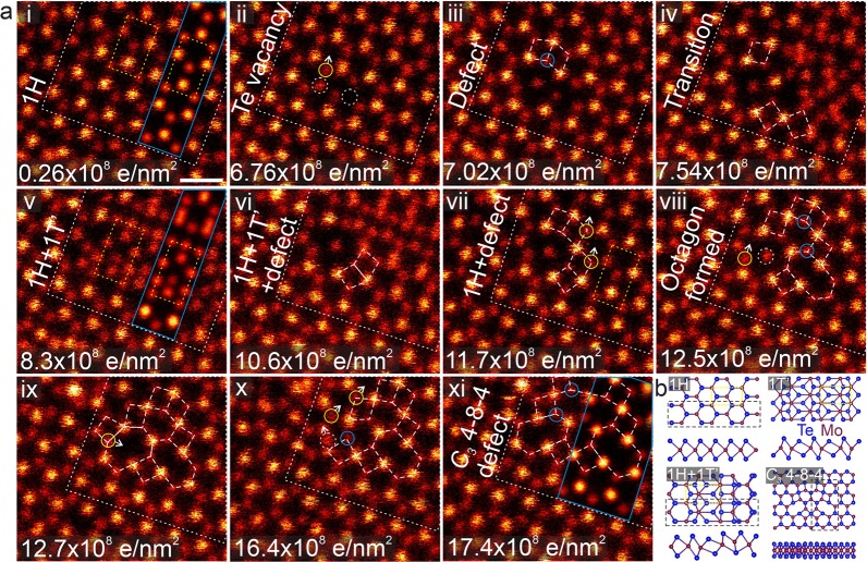
As with other TMDCs,27−29 MoTe2 monolayers damage quickly under electron irradiation (see Supplementary Figure 1). Nevertheless, it is possible to obtain atomic-resolution images of the structure when the exposure of the material is minimized. In Figure 1a we show an image sequence displaying initially a nearly perfect 1H structure, which is then partially converted into a 1T′ phase in panel a-v (after an additional electron dose of ∼8.1 × 10⁸e–/nm2). The energy difference between 1H and 1T′ is just 0.03 eV/atom (see Supplementary Table 1) at zero pressure, and 1T′ becomes favored under strains between 0.3% and 3% at room temperature.9 Hence, the local strain induced by the initially created Te vacancies (at a dose of ∼6.8 × 10⁸e–/nm2) most likely serves as the driving force for the observed transition from 1H to 1T′. After the vacancies have been created, some Mo atoms close to the defect shift to create diamond-shaped 4-membered rings. This leads eventually to the creation of a mixed 1H-1T′ area (after a dose of ∼8.3 × 10⁸e–/nm2). Further exposure to electron irradiation leads first to the creation of vacancies in the 1T′ phase and finally to its disappearance. Afterward, only the defected 1H phase remains. After a dose of ∼12.5 × 10⁸e–/nm2, an 8-membered ring appears in addition to the diamond-shaped ones. At the end of the image sequence, a structure consistent with a 3-fold rotationally symmetric (C3) defect made of 4-8-4-membered rings has been created.
Figure 1.
Phase transition and a 3-fold rotationally symmetric defect in a MoTe2 monolayer. (a) STEM-HAADF image sequence showing two phase transitions (1H → 1T′ and 1T′ → 1H) under electron irradiation. The overlaid areas outlined by blue lines in panels a-i, a-v, and a-xi are simulated images using the black dashed regions of the models in panel b. Images without overlays are shown in Supplementary Figure 2. The unit cells of the 1H and 1T′ phases are marked by yellow dashed frames. Te vacancies are marked by white dashed circles, while the Mo atom, before and after it shifts, is marked with yellow and blue solid circles, respectively. The areas surrounded by the white dashed lines show the same region in all frames. The experimental images display raw data in false color, and the scale bar is 0.5 nm.
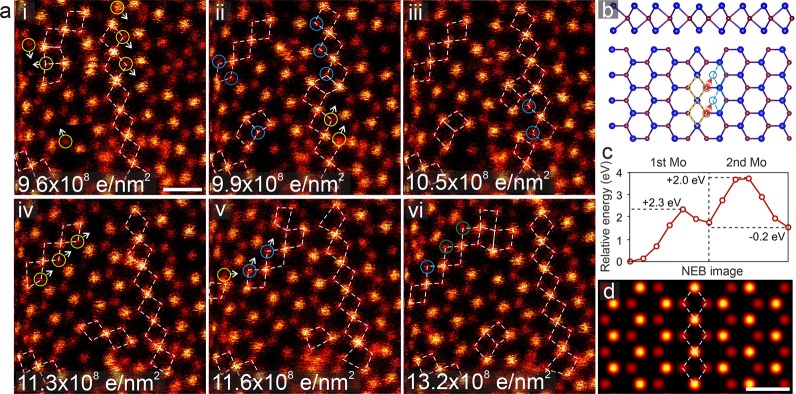
In another image sequence (Figure 2), we show a mirror-symmetric grain boundary between two 1H grains at ∼60° misorientation, similar to what has been reported in MoS2, MoSe2, and MoTe2/MoS2 heterostructures.22−24,30 At least in our case, the area around the boundary was initially a single-crystalline area of 1H, and the misoriented grains only appeared during the experiment (see also Supplementary Figures 3, 4, and 5). During the image sequence (Figure 2), molybdenum atoms at the grain boundary (typically) undergo correlated migration by half a lattice vector (see for example the three atoms marked yellow in Figure 2a-i where the arrow indicates the direction of movement; the new positions are marked in panel a-ii with blue circles), allowing the migration of the grain boundary within the crystal. According to our density functional theory (DFT) simulations (Methods), the migration of the first Mo atom at the boundary has an energy barrier of 2.3 eV, dropping to 2.0 eV for the second one. The migration of the mirror-symmetric grain boundaries in MoTe2 starts with the displacement of Mo atoms by half a lattice vector, which is similar to the grain boundary migration in MoSe2.31 In both materials, chalcogen vacancies are formed in the lattice by electron irradiation before Mo atoms shift to stabilize the system. However, for the grain boundaries in WSe217 and WS232 the migration starts with the movements of chalcogen atoms around the dislocation core in contrast to MoTe2 and MoSe2.
Figure 2.
Migration of grain boundaries in a MoTe2 monolayer. (a) STEM-HAADF image sequence showing the migration of grain boundaries. The arrows on the images show the direction of movement of the Mo atoms marked with circles. (b) Simulated model of the grain boundary. The migration of the boundary atoms is schematically indicated with arrows, similar to the experimental images. (c) Migration barriers for two of the Mo atoms at a four-unit model of the grain boundary calculated via DFT using the nudged elastic band method. (d) Image simulation of the grain boundary model. The experimental images display raw data in false color, and the scale bars are 0.5 nm.
Quantum Dots
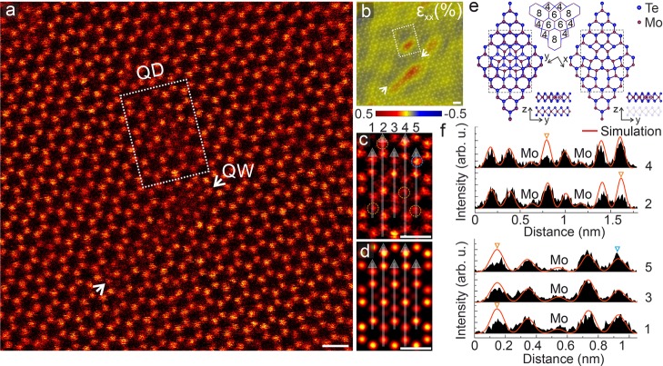
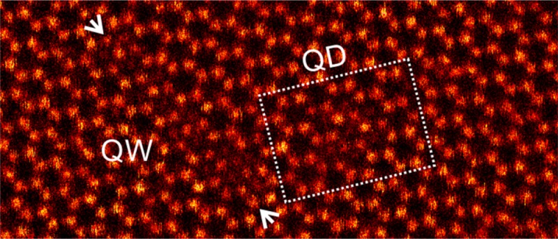
One of the most commonly observed defects in our samples is a QD structure shown for an encapsulated bilayer in Figure 3 (graphene is not visible due to the low contrast of C atoms as compared to Mo and Te; see also Supplementary Figure 6). We observed a concentration of 0.58/100 nm2 for the QDs (total area of 9500 nm2 was imaged). This defect appears as an ca. 1 nm round feature within the 2H phase. Because of the different atomic structure with respect to the surrounding crystal, the QD can also be visualized through geometric phase analysis (along with the resulting strain maps, see Figure 3b). Within the QD, the atomic structure has the appearance of the 1T phase. To ascertain the actual atomic structure, we created a large number of candidate structures for the defects and simulated STEM images based on DFT-relaxed atomic configurations. The best match to the experimental images was obtained for the structure shown in Figure 3. In this structure, one of the layers of the bilayer MoTe2 involves a 3-fold rotationally symmetric defect consisting of 4-8-4-membered rings, whereas the other layer is pristine. This defect is similar to that found in the nonencapsulated material after extensive electron-beam irradiation (Figure 1a-xi). An atomic model of the defected layer is shown in panel e. Intensity profiles recorded on the white lines over the simulated (panel d) and experimental images (panel c) show that the atomic model and the experimental image are in a good agreement. The intensity profiles also reveal that there are Te vacancies and one additional atom in this experimental QD structure as compared to the model (such irregularities, appearing at different atoms for each defect, are common among all the QD structures we observed). Unlike defects created by electron irradiation, these defects in one layer of the encapsulated MoTe2 bilayer are likely to have been formed during sample growth or preparation since they were observed from the beginning of the imaging and formation of additional QDs was only very rarely observed during the experiments.
Figure 3.
Structure of defects in encapsulated bilayer MoTe2. (a) STEM-HAADF image of an encapsulated MoTe2 bilayer with a QD defect (white dashed rectangle) and QW (marked by arrows). Image background has been subtracted using a Gaussian blur with a radius of 20 px. (b) εxx strain map of panel a overlaid on the atomic structure. (c) A close-up of the QD (treated by a Gaussian blur with a radius of 1 px). Orange and blue dashed circles show atomic vacancies and additional atoms, respectively. (d) Image simulation for the atomic model shown in panel e. (e) QD model with and without the second MoTe2 layer. Top views of the QD atomic model with a 3-fold rotationally symmetric defect consisting of 4-8-4-membered rings in the upper MoTe2 layer. (f) Intensity profiles along the white semitransparent arrows shown in panels c and d. Triangles show the locations of atomic vacancies and additional atoms as indicated in panel c. The scale bars are 0.5 nm.
Quantum Wires
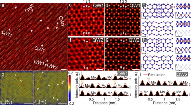
Besides the QD structures, our encapsulated samples also contain two different kinds of QWs (one was visible in Figure 3a). Several examples of both are shown in Figure 4. The concentration of QWs (0.48/100 nm2 in a total observed area of 9500 nm2) is slightly lower than that of the QDs, and they can also be easily detected from microscopy images through strain maps (Figure 4b), either in εxx or εyy depending on the direction of the QW with respect to the host lattice. A close-up image of the first type (QW1) is shown in Figure 4c along with a simulated image (Figure 4d) and the corresponding atomic structure (Figure 4e); QW2 is similarly displayed in Figure 4f-h. The atomic structures of the defects are shown in Figure 4e,h. QW1 includes reflection symmetric (σv∥) units consisting of 8-4-membered rings (Figure 4e). In contrast, QW2 is made of 2-fold rotational symmetric units (C2) also consisting of 8-4-membered rings (Figure 4h). Line profiles over the experimental and simulated STEM-HAADF images are plotted in Figure 4i,j. Similarly to QDs, QW structures also include Te vacancies. QD and QW defects are less stable compared to pristine 1H-MoTe2, and their formation energies are found to be 2.80, 4.81, and 3.73 eV respectively for QD, QW1, and QW2 (see also Supplementary Table 2). Among these defect structures, QD has one more Mo atom than a pristine structure of the same size, whereas the QWs are stoichiometric. The formation energy of the QD has thus been calculated using the chemical potential for bulk molybdenum. Line defects in the armchair direction were previously reported for few-layer MoTe2.33 In that work, it was concluded that line defects are mostly observed in only one of the MoTe2 layers within the few-layer structures, similar to the defects reported here. Further, it was suggested that line defects are formed via the rearrangement of Te vacancies. By contrast, the line defects discussed in our study are formed via the rearrangement of Mo atoms.
Figure 4.
Atomic structure of quantum wires. (a) STEM-HAADF image of several QWs in encapsulated bilayer MoTe2. Image background has been subtracted using a Gaussian blur with a radius of 12 px. The scale bar is 2 nm. (b) εxx and εyy strain maps of panel (a). The scale bar is 4 nm. (c,f) Close-up images of the two different QW structures (treated by a Gaussian blur with a radius of 3 px). Orange dashed circles show atomic vacancies. (d,g) Simulated images corresponding to the experimental structures. The scale bars are 0.5 nm. (e,h) Atomic models of the simulated images (top: both layers, bottom: only the defective layer). (i,j) Intensity profiles along the white arrows on the experimental and simulated QW images. Triangles show the locations of atomic vacancies as indicated in panels (c) and (f).
Evolution of QD and QW Structures during Observation
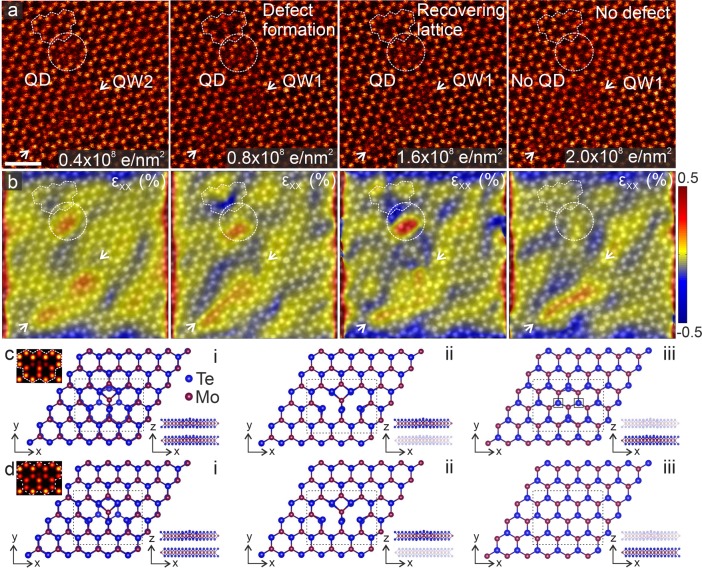
Figure 5 shows an image sequence of an area containing both a QD and a QW (initially having the QW2 structure). Strain maps corresponding to the image sequence in Figure 5a are shown in Figure 5b. Although the QW is barely visible in these strain maps due to its orientation, the QD is easily visible. After an additional electron dose of ∼0.4 × 10⁸e–/nm2, a vacancy defect appears next to the QD. At the same time, presumably due to the negative strain (increasing blue area), the QW structure is transformed from a 2-fold rotation-symmetric type (QW2) to a reflection-symmetric (QW1) type. Although the defect structure in the second frame is a bit unclear, it appears to involve one slightly displaced Mo atom, two missing Te, and one missing Mo, as shown in panel c-i. To further understand this structure, we created two possible atomic models, as shown in panels c,d. While the first layer in panel c-ii involves one shifted and one missing Mo atom, the second layer in panel c-iii has two missing Te atoms. The other model (panel d-i) has no missing Te atoms at the second layer. From the simulated images of both models (see insets of panels c-i and d-i), we conclude that the structure with two missing Te atoms at the second MoTe2 layer is in better agreement with the experimental image. In the third frame of panel a, the displaced Mo atom has moved back to its lattice position. Finally, in the last frame, both Mo and Te vacancies are filled, and at the same time the QD disappears. Another example of atomic dynamics at a QD is shown in Supplementary Figure 7.
Figure 5.
Dynamics of QDs and QWs under electron irradiation. (a) STEM-HAADF image sequence showing the change of the atomic structure of a QD and QW in encapsulated bilayer MoTe2 (background subtracted using a Gaussian blur of 20 px). The scale bar is 0.5 nm. (b) εxx strain maps corresponding to panel a. (c,d) Atomic models of the butterfly-like defect in the second frame of panel a. The areas marked by dashed black frames correspond to those shown in simulated images in the insets. The black squares show the location of Te vacancies at the second MoTe2 layer shown in panel c-iii.
Electronic Structure
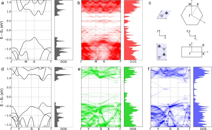
Since both of the observed defect types are created within the semiconducting 1H phase, it is worth asking whether their electronic properties differ significantly from those of the host structure. The electronic band structures calculated for the 1H phase both in the primitive hexagonal 3-atom and orthorhombic 6-atom unit cells are shown in Figure 6a and d. The DFT band gap is ca. 1.14 eV. The unfolded electronic band structures for the QD (hexagonal supercell) and QWs (orthorhombic supercells) are shown in panels b, e, and f. While the extra bands due to the QD defect resemble localized molecular states, in both the QW1 and QW2 defects there is clear evidence for metallic conduction in the direction of the defect line. This suggests the possibility of applications as conductive wires or nanoscale antennas.
Figure 6.
Unfolded electronic band structures calculated with DFT. The band structure (hexagonal cell) of the (a) 1H phase of monolayer MoTe2 and (b) QD defect. (c) The lattice and the first Brillouin zone of the 3-atom and 6-atom unit cells. The electronic band structure (orthorhombic cell) of the (d) 1H phase of monolayer MoTe2, (e) QW1 defect, and (f) QW2 defect. The intensity of some of the bands (in panels b, e, and f) is weaker because these states are due to the localized defect in the unfolded band structure, and the segmentation of the lines reflect the finite k-point sampling.
Edge Structure
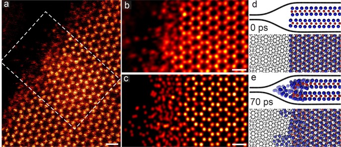
Finally, despite the overall stability of the encapsulated MoTe2 under the electron beam, its edges appear unstable. Figure 7a shows the atomic structure of an edge in bilayer MoTe2. Ideal symmetric edges would be terminated either by Te or Mo atoms. However, elemental identification at the edge is complicated by the liquid-like behavior of the structure during continuous imaging (see Supplementary Videos and Supplementary Figure 8). This is in contrast to the nonencapsulated structure, for which the atomic structure remains ordered (see Supplementary Figure 9). To elucidate on the disordered structure, we carried out molecular dynamics simulations of an encapsulated MoTe2 structure at room temperature. These simulations reveal a clear tendency for the Te atoms to detach from the MoTe2 crystal and spread between the graphene sheets. Interestingly, no electron-beam effect is required to produce this behavior. Due to the similarity between the experimental image (Figure 7b) and the simulated one (Figure 7c) we believe that Te atoms are also responsible for the dynamics observed in the microscope. Following ref (34), we estimate the pressure due to graphene encapsulation to be in the order of a few GPa close to the edge of the MoTe2 structure. In contrast to our present results with MoTe2, graphene-encapsulated MoS2 has been reported to have an easily resolvable edge structure.27,35
Figure 7.
Edge structure of encapsulated bilayer MoTe2. (a) STEM-HAADF image showing the edge of graphene-encapsulated bilayer MoTe2. The image displays raw data in false color. (b) A close-up of the region indicated by the white dashed line in panel a. The image has been treated by a Gaussian blur with a radius of 4 px. (c) Simulated snapshot of graphene-encapsulated bilayer MoTe2 after 70 ps at 300 K. The scale bars are 0.5 nm. (d, e) Side and top views of the model structure at the beginning of the simulation and after 70 ps at 300 K.
Conclusions
Unprotected MoTe2 is highly susceptible to damage during TEM imaging, which leads to the creation of vacancies, especially at the edges of the suspended material, but also to interesting atomic-scale dynamics. For example, the semiconducting 1H phase can be locally turned into the semimetallic 1T′ phase, which can in turn be transformed back to defective 2H due to continuing loss of atoms. Electron irradiation also leads to the migration of grain boundaries between 1H grains with a 60° misorientation. Further, a 3-fold rotationally symmetric defect appears at high electron doses. All of these dynamics are significantly suppressed when MoTe2 is encapsulated between two graphene layers, which allows the study of its intrinsic defects. We observe a relatively high concentration (0.58/100 nm2) of 1 nm-sized quantum dot structures, associated with the 3-fold rotationally symmetric defect, as well as two different quantum wire structures (with a joint concentration of about 0.48/100 nm2): a reflection-symmetric defect (QW1) and 2-fold rotationally symmetric defect (QW2). Both the possibility of introducing phase transitions between electrically very different phases and the existence of quantum dot and quantum wire defects with midgap states in the otherwise semiconducting material indicate a possibility for tuning the material properties through defect engineering. The amorphous nature of the edge in encapsulated MoTe2 can lead to transport of Te atoms through the edge, and thus a metallic Te ion channel surrounding the semiconducting MoTe2 can be obtained.
Methods
Sample Preparation
The MoTe2 flakes were exfoliated on a SiO2/Si substrate and then transferred onto TEM grids with a carbon-based support membrane (QUANTIFOIL). Monolayer graphene sheets were synthesized by chemical vapor deposition in a mixture of 50 sccm CH4 and 2000 sccm Ar/H2 gases at 960 °C. First, a graphene sheet was transferred from Cu foil onto a TEM grid without polymer, and then the MoTe2 flakes were transferred on top. The obtained MoTe2/graphene stack was then transferred onto another graphene sheet on Cu foil. The Cu foils were etched with FeCl3.
Transmission Electron Microscopy
STEM images of MoTe2 and graphene-encapsulated MoTe2 were recorded using a Nion UltraSTEM 100 electron microscope operated at a 60 kV accelerating voltage in near ultrahigh vacuum (2 × 10⁻⁷ Pa) using the high angle annular dark field (HAADF) detector with a collection angle of 80–200 mrad. For TEM diffraction experiments (Supporting Information) we used a Delong instruments LVEM5 table-top transmission electron microscope operated at 5 kV.
DFT and STEM Image Simulations
Density functional theory (DFT) simulations were carried out using the grid-based projector-augmented wave (GPAW) software package36 to study the properties of the unit cell and supercells of monolayer and bilayer MoTe2. For unit cells, we used a plane-wave basis (cutoff energy 700 eV, 16 × 16 × 1 k-point mesh) to relax the atomic positions using the C09 van der Waals functional37 (the DF2 functional38 was additionally used for relative energies of different MoTe2 phases shown in Supplementary Table 1). The atomic structure of supercells of MoTe2 including QDs and QWs was relaxed with periodic boundary conditions in the finite-difference mode with the grid spacing of 0.2 Å and a 3 × 3 × 1 k-point mesh so that maximum forces were <0.05 eV Å–1. A double-ζ linear combination of atomic orbitals basis was used to speed up the calculations for the larger simulated structures. STEM-HAADF and TEM diffraction simulations were performed using the QSTEM software with parameters corresponding to the experiments.39 The NEB simulation was performed with no frozen atoms and with five intermediate images.40 All optimized atomic structures are provided in the Supporting Information.
Molecular Dynamics
To study the atomic structure of MoTe2 edges encapsulated by graphene, we created a supercell with a size of 28 × 58 Å2 of bilayer 2H MoTe2. The two graphene sheets are misoriented by ∼18° with respect to each other, and the resulting moiré pattern periodicity is ∼14 Å. The reactive bond-order-dependent force field that supports bond breaking and bond formation was used to describe the interaction between molybdenum and tellurium atoms and also the interaction between the carbon atoms.41,42 Long distance van der Waals interactions between the carbon atoms and between C–Mo and C–Te were treated with Morse potentials. All calculations were performed with Large-scale Atomic/Molecular Massively Parallel Simulator (LAMMPS) code.43,44 The total potential energy was minimized by relaxing both layers without applying any constraints until the forces were below 10–3 eV/Å and the strain on the whole structure was negligible (pressure below 1 bar). Later, the temperature was increased to 300 K for 1 ns for the molecular dynamics simulations (graphene sheets were kept at 0 K).
Acknowledgments
K.E., M.R.A.M., and J.C.M. acknowledge support from the Austrian Science Fund (FWF) through project P25721-N20, T.S. acknowledges support through project P 28322-N36, and M.R.A.M. and J.K. acknowledge support through project I3181-N36. T.J.P. was supported by the European Union’s Horizon 2020 research and innovation programme under the Marie Skłodowska-Curie grant agreement No. 655760-DIGIPHASE. J.C.M. acknowledges funding by the European Research Council Grant No. 336453-PICOMAT, and J.K. acknowledges funding from the Wiener Wissenschafts-, Forschungs- und Technologiefonds (WWTF) via project MA14-009. We also acknowledge generous computational resources from the Vienna Scientific Cluster.
Supporting Information Available
The Supporting Information is available free of charge on the ACS Publications website at DOI: 10.1021/acs.chemmater.7b03760.
TEM and electron diffraction images, STEM-HAADF images of monolayer, bilayer and encapsulated MoTe2, the atomic model of graphene-encapsulated MoTe2 monolayer, DFT total energies of 2H, 1T, and 1T′ phases of MoTe2 monolayers and bilayers, formation energies of monolayer MoTe2 defects (PDF)
Atomic configuration files of the structures shown in the manuscript (ZIP)
Videos showing the edge of graphene-encapsulated MoTe2 bilayer (ZIP)
The authors declare no competing financial interest.
Supplementary Material
References
- Susi T.; Meyer J. C.; Kotakoski J. Manipulating low-dimensional materials down to the level of single atoms with electron irradiation. Ultramicroscopy 2017, 180, 163–172. 10.1016/j.ultramic.2017.03.005. [DOI] [PubMed] [Google Scholar]
- Deng K.; et al. Experimental observation of topological Fermi arcs in type-II Weyl semimetal MoTe2. Nat. Phys. 2016, 12, 1105–1110. 10.1038/nphys3871. [DOI] [Google Scholar]
- Han G. H.; Hoon Keum D.; Zhao J.; Gyu Shin B.; Song S.; Jun Bae J.; Lee J.; Ho Kim J.; Kim H.; Hee Moon B.; Hee Lee Y. Absorption dichroism of monolayer 1T′-MoTe2 in visible range. 2D Mater. 2016, 3, 031010. 10.1088/2053-1583/3/3/031010. [DOI] [Google Scholar]
- Joshi J.; Stone I. R.; Beams R.; Krylyuk S.; Kalish I.; Davydov A. V.; Vora P. M. Phonon anharmonicity in bulk Td-MoTe2. Appl. Phys. Lett. 2016, 109, 031903. 10.1063/1.4959099. [DOI] [PMC free article] [PubMed] [Google Scholar]
- Diaz H. C.; Chaghi R.; Ma Y.; Batzill M. Molecular beam epitaxy of the Van der Waals heterostructure MoTe2 on MoS2: phase, thermal, and chemical stability. 2D Mater. 2015, 2, 044010. 10.1088/2053-1583/2/4/044010. [DOI] [Google Scholar]
- Keum D. H.; Cho S.; Kim J. H.; Choe D.-H.; Sung H.-J.; Kan M.; Kang H.; Hwang J.-Y.; Kim S. W.; Yang H.; Chang K. J.; Lee Y. H. Bandgap opening in few-layered monoclinic MoTe2. Nat. Phys. 2015, 11, 482–486. 10.1038/nphys3314. [DOI] [Google Scholar]
- Kuiri M.; Chakraborty B.; Paul A.; Das S.; Sood A. K.; Das A. Enhancing photoresponsivity using MoTe2-graphene vertical heterostructures. Appl. Phys. Lett. 2016, 108, 063506. 10.1063/1.4941996. [DOI] [Google Scholar]
- Park J. C.; Yun S. J.; Kim H.; Park J. H.; Chae S. H.; An S. J.; Kim J. G.; Kim S. M.; Kim K. K.; Lee Y. H. Phase-engineered synthesis of centimeter-scale 1T- and 2H-molybdenum ditelluride thin films. ACS Nano 2015, 9, 6548–6554. 10.1021/acsnano.5b02511. [DOI] [PubMed] [Google Scholar]
- Duerloo K.-A. N.; Li Y.; Reed E. J. Structural phase transitions in two-dimensional Mo- and W-dichalcogenide monolayers. Nat. Commun. 2014, 5, 4214. 10.1038/ncomms5214. [DOI] [PubMed] [Google Scholar]
- Sun Y.; Wu S. C.; Ali M. N.; Felser C.; Yan B. Prediction of Weyl semimetal in orthorhombic MoTe2. Phys. Rev. B: Condens. Matter Mater. Phys. 2015, 92, 161107. 10.1103/PhysRevB.92.161107. [DOI] [Google Scholar]
- Li Y.; Duerloo K.-A. N.; Wauson K.; Reed E. J. Structural semiconductor-to-semimetal phase transition in two-dimensional materials induced by electrostatic gating. Nat. Commun. 2016, 7, 10671. 10.1038/ncomms10671. [DOI] [PMC free article] [PubMed] [Google Scholar]
- Huang H. H.; Fan X.; Singh D. J.; Chen H.; Jiang Q.; Zheng W. T. Controlling phase transition for single-layer MTe2 (M = Mo and W): modulation of the potential barrier under strain. Phys. Chem. Chem. Phys. 2016, 18, 4086–4094. 10.1039/C5CP06706E. [DOI] [PubMed] [Google Scholar]
- Cho S.; Kim S.; Kim J. H.; Zhao J.; Seok J.; Keum D. H.; Baik J.; Choe D.-h.; Chang K. J.; Suenaga K.; Kim S. W.; Lee Y. H.; Yang H. Phase patterning for ohmic homojunction contact in MoTe2. Science 2015, 349, 625–628. 10.1126/science.aab3175. [DOI] [PubMed] [Google Scholar]
- Song S.; Keum D. H.; Cho S.; Perello D.; Kim Y.; Lee Y. H. Room Temperature Semiconductor-Metal Transition of MoTe2 Thin Films Engineered by Strain. Nano Lett. 2016, 16, 188–193. 10.1021/acs.nanolett.5b03481. [DOI] [PubMed] [Google Scholar]
- Zhang K.; Bao C.; Gu Q.; Ren X.; Zhang H.; Deng K.; Wu Y.; Li Y.; Feng J.; Zhou S. Raman signatures of inversion symmetry breaking and structural phase transition in type-II Weyl semimetal MoTe2. Nat. Commun. 2016, 7, 13552. 10.1038/ncomms13552. [DOI] [PMC free article] [PubMed] [Google Scholar]
- Lin Z.; Carvalho B. R.; Kahn E.; Lv R.; Rao R.; Terrones H.; Pimenta M. A.; Terrones M. Defect engineering of two-dimensional transition metal dichalcogenides. 2D Mater. 2016, 3, 022002. 10.1088/2053-1583/3/2/022002. [DOI] [Google Scholar]
- Lin Y.-C.; Björkman T.; Komsa H.-P.; Teng P.-Y.; Yeh C.-H.; Huang F.-S.; Lin K.-H.; Jadczak J.; Huang Y.-S.; Chiu P.-W.; Krasheninnikov A. V.; Suenaga K. Three-fold rotational defects in two-dimensional transition metal dichalcogenides. Nat. Commun. 2015, 6, 6736. 10.1038/ncomms7736. [DOI] [PMC free article] [PubMed] [Google Scholar]
- Enyashin A. N.; Bar-sadan M.; Houben L.; Seifert G. Line defects in molybdenum disulfide layers. J. Phys. Chem. C 2013, 117, 10842–10848. 10.1021/jp403976d. [DOI] [Google Scholar]
- Ghorbani-Asl M.; Enyashin A. N.; Kuc A.; Seifert G.; Heine T. Defect-induced conductivity anisotropy in MoS2 monolayers. Phys. Rev. B: Condens. Matter Mater. Phys. 2013, 88, 245440. 10.1103/PhysRevB.88.245440. [DOI] [Google Scholar]
- van der Zande A. M.; Huang P. Y.; Chenet D. A.; Berkelbach T. C.; You Y.; Lee G.-H.; Heinz T. F.; Reichman D. R.; Muller D. A.; Hone J. C. Grains and grain boundaries in highly crystalline monolayer molybdenum disulphide. Nat. Mater. 2013, 12, 554–561. 10.1038/nmat3633. [DOI] [PubMed] [Google Scholar]
- Dumcenco D.; Ovchinnikov D.; Lopez Sanchez O.; Gillet P.; Alexander D. T. L.; Lazar S.; Radenovic A.; Kis A. Large-area MoS2 grown using H2S as the sulfur source. 2D Mater. 2015, 2, 044005. 10.1088/2053-1583/2/4/044005. [DOI] [Google Scholar]
- Ma Y.; Kolekar S.; Coy Diaz H.; Aprojanz J.; Miccoli I.; Tegenkamp C.; Batzill M. Metallic twin grain boundaries embedded in MoSe2 monolayers grown by molecular beam epitaxy. ACS Nano 2017, 11, 5130–5139. 10.1021/acsnano.7b02172. [DOI] [PubMed] [Google Scholar]
- Diaz H. C.; Ma Y.; Chaghi R.; Batzill M. High density of (pseudo) periodic twin-grain boundaries in molecular beam epitaxy-grown van der Waals heterostructure: MoTe2/MoS2. Appl. Phys. Lett. 2016, 108, 191606. 10.1063/1.4949559. [DOI] [Google Scholar]
- Zhou W.; Zou X.; Najmaei S.; Liu Z.; Shi Y.; Kong J.; Lou J.; Ajayan P. M.; Yakobson B. I.; Idrobo J.-C. Intrinsic Structural Defects in Monolayer Molybdenum Disulfide. Nano Lett. 2013, 13, 2615–2622. 10.1021/nl4007479. [DOI] [PubMed] [Google Scholar]
- Wang Q. H.; Kalantar-Zadeh K.; Kis A.; Coleman J. N.; Strano M. S. Electronics and optoelectronics of two-dimensional transition metal dichalcogenides. Nat. Nanotechnol. 2012, 7, 699–712. 10.1038/nnano.2012.193. [DOI] [PubMed] [Google Scholar]
- Zhang Z.; Zou X.; Crespi V. H.; Yakobson B. I. Intrinsic magnetism of grain boundaries in two-dimensional metal dichalcogenides. ACS Nano 2013, 7, 10475–10481. 10.1021/nn4052887. [DOI] [PubMed] [Google Scholar]
- Zan R.; Ramasse Q. M.; Jalil R.; Georgiou T.; Bangert U.; Novoselov K. S. Control of radiation damage in MoS2 by graphene encapsulation. ACS Nano 2013, 7, 10167–10174. 10.1021/nn4044035. [DOI] [PubMed] [Google Scholar]
- Nguyen L.; Komsa H.-P.; Khestanova E.; Kashtiban R. J.; Peters J. J. P.; Lawlor S.; Sanchez A. M.; Sloan J.; Gorbachev R. V.; Grigorieva I. V.; Krasheninnikov A. V.; Haigh S. J. Atomic defects and doping of monolayer NbSe2. ACS Nano 2017, 11, 2894–2904. 10.1021/acsnano.6b08036. [DOI] [PubMed] [Google Scholar]
- Iberi V.; Liang L.; Ievlev A. V.; Stanford M. G.; Lin M.-W.; Li X.; Mahjouri-Samani M.; Jesse S.; Sumpter B. G.; Kalinin S. V.; Joy D. C.; Xiao K.; Belianinov A.; Ovchinnikova O. S. Nanoforging single layer MoSe2 through defect engineering with focused helium ion beams. Sci. Rep. 2016, 6, 30481. 10.1038/srep30481. [DOI] [PMC free article] [PubMed] [Google Scholar]
- Hong J.; Wang Y.; Wang A.; Lv D.; Jin C.; Xu Z.; Probert M. I. J.; Yuan J.; Zhang Z. Atomistic dynamics of sulfur-deficient high-symmetry grain boundaries in molybdenum disulfide. Nanoscale 2017, 9, 10312–10320. 10.1039/C7NR02941A. [DOI] [PubMed] [Google Scholar]
- Lin J.; Pantelides S. T.; Zhou W. Vacancy-Induced Formation and Growth of Inversion Domains in Transition-Metal Dichalcogenide Monolayer. ACS Nano 2015, 9, 5189–5197. 10.1021/acsnano.5b00554. [DOI] [PubMed] [Google Scholar]
- Azizi A.; Zou X.; Ercius P.; Zhang Z.; Elías A. L.; Perea-López N.; Stone G.; Terrones M.; Yakobson B. I.; Alem N. Dislocation motion and grain boundary migration in two-dimensional tungsten disulphide. Nat. Commun. 2014, 5, 4867. 10.1038/ncomms5867. [DOI] [PubMed] [Google Scholar]
- Zhao J.; Nam H.; Ly T. H.; Yun S. J.; Kim S.; Cho S.; Yang H.; Lee Y. H. Chain Vacancies in 2D Crystals. Small 2017, 13, 1601930. 10.1002/smll.201601930. [DOI] [PubMed] [Google Scholar]
- Vasu K. S.; Prestat E.; Abraham J.; Dix J.; Kashtiban R. J.; Beheshtian J.; Sloan J.; Carbone P.; Neek-Amal M.; Haigh S. J.; Geim A. K.; Nair R. R. Van der Waals pressure and its effect on trapped interlayer molecules. Nat. Commun. 2016, 7, 12168. 10.1038/ncomms12168. [DOI] [PMC free article] [PubMed] [Google Scholar]
- Algara-Siller G.; Kurasch S.; Sedighi M.; Lehtinen O.; Kaiser U. The pristine atomic structure of MoS2 monolayer protected from electron radiation damage by graphene. Appl. Phys. Lett. 2013, 103, 203107. 10.1063/1.4830036. [DOI] [Google Scholar]
- Mortensen J. J.; Hansen L. B.; Jacobsen K. W. Real-space grid implementation of the projector augmented wave method. Phys. Rev. B: Condens. Matter Mater. Phys. 2005, 71, 035109. 10.1103/PhysRevB.71.035109. [DOI] [Google Scholar]
- Cooper V. R. Van der Waals density functional: An appropriate exchange functional. Phys. Rev. B: Condens. Matter Mater. Phys. 2010, 81, 161104. 10.1103/PhysRevB.81.161104. [DOI] [Google Scholar]
- Lee K.; Murray É. D.; Kong L.; Lundqvist B. I.; Langreth D. C. Higher-accuracy van der Waals density functional. Phys. Rev. B: Condens. Matter Mater. Phys. 2010, 82, 081101. 10.1103/PhysRevB.82.081101. [DOI] [Google Scholar]
- Koch C.Determinations of core structure periodicity and point defect density along dislocations, Dissertation, 2002. [Google Scholar]
- Henkelman G.; Jonsson H. Improved tangent estimate in the nudged elastic band method for finding minimum energy paths and saddle points. J. Chem. Phys. 2000, 113, 9978–9985. 10.1063/1.1323224. [DOI] [Google Scholar]
- Aktulga H.; Fogarty J.; Pandit S.; Grama A. Parallel reactive molecular dynamics: Numerical methods and algorithmic techniques. Parallel Comput. 2012, 38, 245–259. 10.1016/j.parco.2011.08.005. [DOI] [Google Scholar]
- Onofrio N.; Guzman D.; Strachan A. The dynamics of copper intercalated molybdenum ditelluride. J. Chem. Phys. 2016, 145, 194702. 10.1063/1.4967808. [DOI] [PubMed] [Google Scholar]
- Plimpton S. Fast Parallel Algorithms for Short-Range Molecular Dynamics. J. Comput. Phys. 1995, 117, 1–19. 10.1006/jcph.1995.1039. [DOI] [Google Scholar]
- Plimpton S. J.; Thompson A. P. Computational aspects of many-body potentials. MRS Bull. 2012, 37, 513–521. 10.1557/mrs.2012.96. [DOI] [Google Scholar]
Associated Data
This section collects any data citations, data availability statements, or supplementary materials included in this article.


