Abstract
In this paper, we investigate the synthesis of WSe2 by chemical vapor deposition and study the current transport and device scaling of monolayer WSe2. We found that the device characteristics of the back-gated WSe2 transistors with thick oxides are very sensitive to the applied drain bias, especially for transistors in the sub-micrometer regime. The threshold voltage, subthreshold swing, and extracted field-effect mobility vary with the applied drain bias. The output characteristics in the long-channel transistors show ohmic-like behavior, while that in the short-channel transistors show Schottky-like behavior. Our investigation reveals that these phenomena are caused by the drain-induced barrier lowering (short-channel effect). For back-gated WSe2 transistors with 280 nm oxide, the short-channel effect appears when the channel length is shorter than 0.4 µm. This extremely long electrostatic scaling length is due to the thick back-gate oxides. In addition, we also found that the hydrogen flow rate and the amount of WO3 precursor play an important role in the morphology of the WSe2. The hole mobility of the monolayer WSe2 is limited by Columbic scattering below 250 K, while it is limited by phonon scattering above 250 K. These findings are very important for the synthesis of WSe2 and accurate characterization of the electronic devices based on 2D materials.
Introduction
WSe2 is an important member of the transition metal dichalcogenide (TMDC) family due to its smaller effective electron and hole masses compared to most of the other TMDCs1, and more importantly due to its ambipolar characteristics2. The small effective mass implies high carrier mobilities. The hole mobility of WSe2 is reported to reach 500 cm2/V-s at room temperature and 2.1 × 103 cm2/V-s at 5 K3,4. The ambipolar conduction is essential for complementary metal-oxide semiconductor (CMOS) circuits such as inverters, since most of the TMDCs (such as MoS2, MoSe2, and WS2), are naturally n-type doped. Although MoTe2 and black phosphorus have also been reported to show p-type conduction5–8, these materials are less stable in ambient conditions. Electrical properties of WSe2 including quantum oscillations, carrier mobilities, contacts, and polarity controls, have been studied and various electronic devices based on WSe2, including metal-oxide field-effect transistors (MOSFETs), tunneling devices, bipolar transistors, and integrated circuits, have been demonstrated2,3,9–22. However, most of these studies focus on exfoliated WSe2 flakes. For practical applications, synthesis of large area WSe2 with controllable layer thickness and quality is essential. There are several recent reports on the growth of thin WSe2 using chemical vapor deposition (CVD)23–26, and metal-organic CVD (MOCVD)27,28. However, study of the electrical transport of CVD grown WSe2 is still lacking. In this paper, we systematically investigate the growth of monolayer WSe2 by CVD and study the current transport of CVD WSe2, including short-channel effect, temperature dependence of carrier mobility, subthreshold swing, and interface states.
Results and Discussion
Synthesis of CVD WSe2
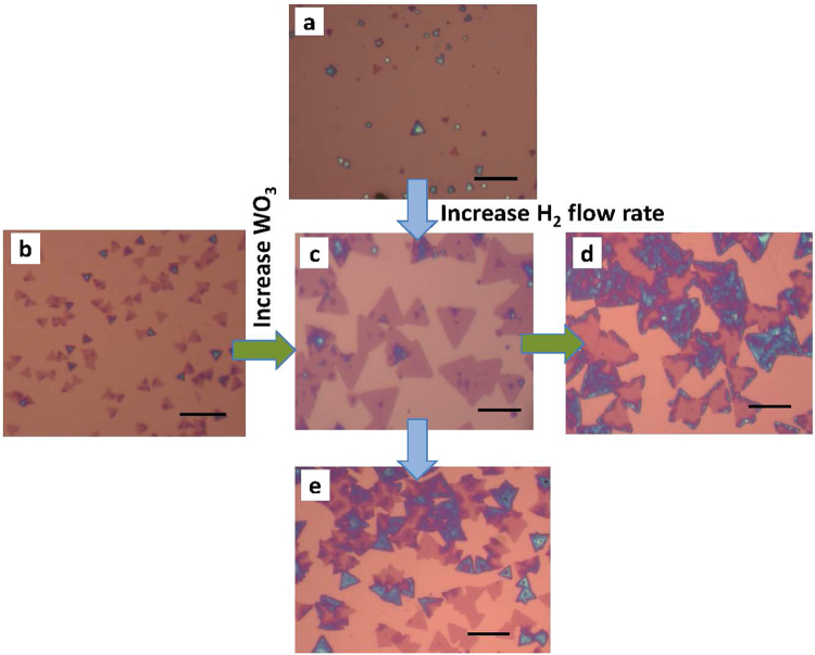
Solid precursor WO3 and Se power were used to synthesize WSe2 on Si/SiO2 substrate in a CVD chamber. Various growth conditions have been investigated, including hydrogen flow rate, WO3 precursor amount, growth temperature, and argon flow rate. We found that these growth parameters can significantly influence the morphology of the WSe2. Figure 1a–e show the optical images of the synthesized WSe2 with various hydrogen flow rates and WO3 precursor amounts. For a given flow rate of argon carrier gas [60 standard cubic centimeters per minute (sccm)], when the hydrogen flow rate increases from 15 sccm to 20 sccm, the grain size of WSe2 increases dramatically. However, when the hydrogen flow rate further increases to 25 sccm, the grain size decreases and multilayer stacks start to form. This is because selenium has very low chemical reactivity. A strong reducer such as hydrogen is needed in the selenization reduction of WO3. However, if the hydrogen flow rate is too high, the reduction of WO3 to W happens very quickly and the WO3 powder only lasts for a very short time, which results in small grains of thick WSe2. The amount of the precursors loaded in the chamber also plays an important role. For a given amount of Se precursor [(300 milligram (mg)], increasing the quantity of WO3 precursor from 100 mg to 150 mg can effectively increase the grain size. However, further increase of WO3 to 200 mg will result in the growth of multi-layer WSe2.
Figure 1.
Optical image of CVD WSe2 grown at various hydrogen flow rates and WO3 precursor amounts: (a) H2 flow rate 15 sccm, WO3 quantity 150 mg; (b) H2 flow rate 20 sccm, WO3 quantity 100 mg; (c) H2 flow rate 20 sccm, WO3 quantity 150 mg; (d) H2 flow rate 20 sccm, WO3 quantity 200 mg; (e) H2 flow rate 25 sccm, WO3 quantity 150 mg. The scale bars in the images are 10 µm.
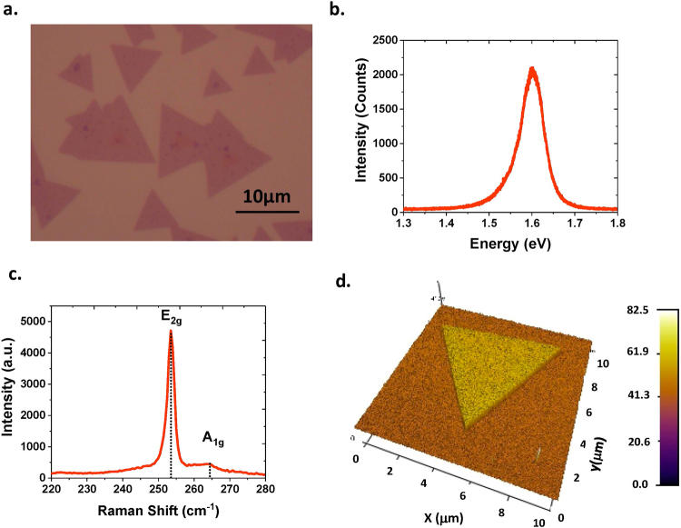
The optimized growth condition for WSe2 using this CVD system is 150 mg of WO3 and 300 mg of Se powder, ambient pressure, 875 °C growth temperature, 70/20 sccm flow of Ar/H2, and 10~15 minutes growth duration. Perylene-3,4,9,10-tetracarboxylic acid tetra potassium (PTAS) was used as the seeding promoter. With the optimized growth condition, high-quality monolayer WSe2 was obtained. Figure 2a–d shows the typical optical image, photoluminescence (PL) spectrum, Raman spectrum, and atomic force microscopy (AFM) phase image of the synthesized WSe2. Bright light emission at ∼1.60 eV and symmetric single PL peak suggest the direct band gap nature of monolayer WSe2, showing good agreement with other recent reports about PL of monolayer WSe224–26,29–32. The E2g and A1g modes in the Raman spectrum are at 253.5 cm−1 and 264.2 cm−1, respectively. Comparing the peak position with the spectrum obtained from the exfoliated monolayer WSe233, we verify that the WSe2 film is monolayer. The AFM phase image shows a clear triangle pattern. From the AFM step height profile, the thickness of the WSe2 is measured as ~0.54 nm, confirming its monolayer character.
Figure 2.
Microscopic characterization of monolayer WSe2. (a) Optical image, (b) Photoluminescence spectrum, (3) Raman spectrum, and (4) AFM phase image.
Device scaling of the back-gated WSe2 transistors
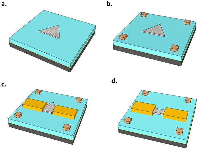
WSe2 transistors with various gate lengths (from 0.1 µm to 5 µm) are fabricated using Pd as metal contacts. Figure 3 illustrated the process flow of the WSe2 devices. The alignment marks with Ti/Au metals were formed by ebeam lithography, metal deposition and lift-off. Hall-bars and transistors were designed for individual WSe2 triangles. The source/drain electrodes (40 nm Pd) were formed by ebeam lithography, metal evaporation and lift-off. The WSe2 channel is defined by ebeam lithography and oxygen plasma etching. The electrical characteristics were measured in vacuum at various temperatures.
Figure 3.
Illustration of the fabrication of the WSe2 devices. (a) Synthesize WSe2 on SiO2/Si substrate using CVD. (b) Form alignment marks using ebeam lithography, metal deposition and lift-off. (c) Form source/drain electrodes using ebeam lithography, metal deposition and lift-off. (d) Define channel by ebeam lithography and oxygen plasma etching.
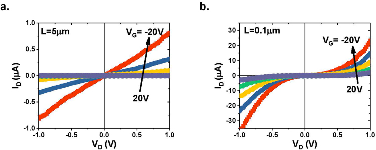
Surprisingly, in long-channel transitions (L = 5 µm), the output characteristics (ID~VD curves) are linear, indicating ohmic contacts, shown in Fig. 4a, while in short-channel transistors (L = 0.1 µm), the ID~VD curves are non-linear, shown in Fig. 4b, resembling Schottky contact characteristics. Since both the long- and short-channel transistors are fabricated on the same wafer with nearly identical WSe2 and Pd metals. It is very unlikely that they formed different types of contacts. Our further investigation reveals that these non-linear output characteristics in the WSe2 transistors are not related to the metal contacts, but due to the short-channel effect, which will be discussed below.
Figure 4.
The output characteristics of the CVD WSe2 transistors with (a) channel length L = 5 µm, and (b) channel length L=0.1 µm.
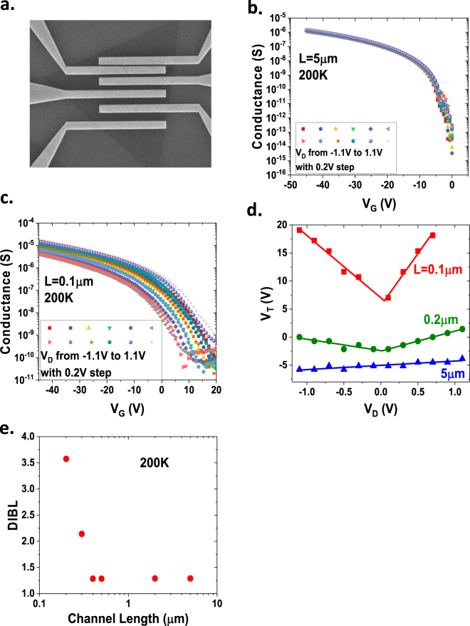
The transfer characteristics (ID~VG curves) were measured at various drain voltages for WSe2 transistors with various gate lengths in a transmission line micro (TLM). A typical SEM image of the TLM structure is shown in Fig. 5a. (Note, in order to avoid the SEM damage on the monolayer WSe2 in the electronic device, the SEM is taken on a neighboring device with same layout on the same wafer as the device tested electrically). The channel conductances at various drain voltages for a long-channel (L = 5 µm) and a short-channel (L = 0.1 µm) transistor, are shown in Fig. 5b and c. For the long-channel transistor, the conductance is nearly independent of the drain voltages. For the short-channel transistor, however, there is a large dispersion of the conductance, especially at the subthreshold regime. Figure 5d plots the threshold voltage as a function of drain voltage for transistors with channel lengths of L = 0.1 μm, 0.2 μm, and 5 μm. We can see that the threshold voltage increases dramatically as the amplitude of the drain voltage, |VD|, increases for the short channels (L = 0.1 μm and 0.2 μm), while it is nearly constant for the long channel (L = 5 μm). This positive shift of the threshold voltage at high drain bias in these short-channel p-type transistors is a result of the fact that the energy barrier between the source and drain is lowered by the high drain voltage and thus the transistors are much easier to turn on. The drain-induced barrier lowering (DIBL) can be estimated using the equation , where is the threshold voltage measured at a supply voltage (high drain voltage), is the threshold voltage measured at a very low drain voltage, VDD is the supply voltage (high drain voltage), is the low drain voltage. Here we use drain biases of 0.1 V and 1.1 V to extract the DIBL. Figure 5e shows the DIBL of the back-gated WSe2 transistor as a function of the channel length. The upturn of the DIBL does not show up until the channel length is shorter than 0.4 µm. Since the back-gate oxide is very thick (280 nm in this case), the electrostatic scaling length is very long. The electrostatic scaling length can be estimated by the equation , where tox is the oxide thickness, ts is the semiconductor thickness, εs is the semiconductor dielectric constant, and εox is the oxide dielectric constant34,35. For the back-gated WSe2 transistors, assuming tox = 280 nm, ts ≈ 0.54 nm, ϵs ≈ 7, and ϵox ≈ 3.9, respectively, the electrostatic scaling length is estimated as λ ≈ 0.064 μm. For a planar device, the minimum channel length needed to preserve the long-channel behavior is typically 4–5 times the electrostatic scaling length, which corresponds to L = 0.26~0.32 μm in this case. This is consistent with our DIBL results, which reveal that the short-channel effect starts to show up when the channel is shorter than 0.4 μm. As the energy barrier between source and drain reduces, the drain current will increase exponentially. This explains the dramatic increase of the drain current at high drain voltages in the ID~VD plots for the short-channel transistors, shown in Fig. 4b.
Figure 5.
Short-channel effect in WSe2 transistors. (a) SEM image of a WSe2 TLM structure consisting of five transistors with various channel lengths. (b) Conductance as a function of gate voltage in a long-channel transistor (L = 5 µm) measured at various drain voltages. (c) Conductance as a function of gate voltage in a short-channel transistor (L = 0.1 µm) measured at various drain voltages. (d) Threshold voltage as a function of drain voltage for WSe2 transistors with various channel lengths from 0.1 µm to 5 µm. (e) Drain-induced barrier lowering (DIBL) of the WSe2 transistors as a function of channel length.
Carrier mobility in CVD WSe2
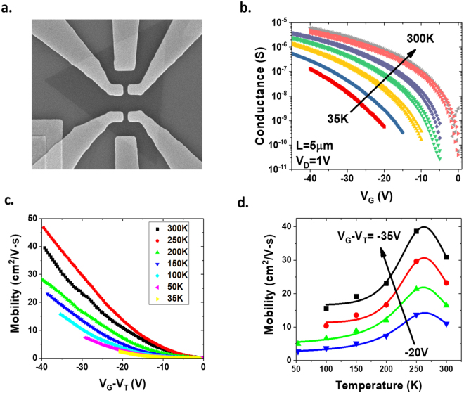
The carrier mobility is an important indicator of the quality of the semiconductor. The carrier mobility of the CVD WSe2 is studied in the long-channel transistors to eliminate the possible short-channel effects, and the conductances were measured using the four-point method to minimize the impact of the contact resistances. Figure 6a shows the SEM image of a typical Hall-bar device. The four-point conductance as a function of gate voltage measured of a WSe2 Hall-bar device at various temperatures is shown in Fig. 6b. Note the SEM and conductance are taken on two separate devices with the same layout on the same wafer to avoid the impact of SEM scan on the electrical performance of the device. The field-effect mobility is extracted from the four-point conductance, using the equation , where σ is the four-point conductance, VG is the gate voltage, W is channel width, L is the channel length, and Cox is the oxide capacitance36. The extracted field effect mobility as a function of gate voltage is shown in Fig. 6c. As the transistor is biased further into the inversion, the mobility increases because of the screening effect due to the inversion charge, which reduces the Coulomb scattering. The temperature dependence of the mobility shows a turn-around behavior at 250 K, shown in Fig. 6d. At low temperatures, the mobility increases with increasing temperature, and at temperatures above 250 K, the mobility decreases with increasing temperature. At low temperatures, Coulomb scattering dominates. When the temperature increases, the carrier velocity increases, which can reduce the influence of the Coulomb scattering from the charged impurities. At high temperatures, phonon scattering dominates. Increasing temperature will increase the lattice vibration and reduce the mobility. Seven Hall-bar devices were measured to determine the mobility and carrier density. At VG − VT = −30 V, i.e. carrier density of ~2.3 × 1012 cm−2, the average mobility is ~24.8 cm2/V-s, the maximum mobility is 46.1 cm2/V-s, and the minimum mobility is 7.9 cm2/V-s. Note, these electrical characteristics were measured after source/drain formation and before the channel is etched into rectangular shape. After the sample experienced additional process steps, including lithography, oxygen plasma etching and resist strip, and additional characterizations such as SEM, the measured mobilities of the Hall-bar devices are significantly lower, as shown in Fig. S1 in the supplementary information. One possible cause of this mobility degradation is that the additional process steps and the high-energy electron beam in SEM degraded the monolayer WSe2 channel. The other possible reason for the lower extracted mobility after channel-cut is that there are parasitic current path in the triangular-shaped channel before the channel-cut, which may cause overestimation of the channel mobility. The gate voltage and temperature dependence of the channel mobilities in a WSe2 Hall-bar devices after channel-cut and SEM scan are shown in Fig. S2. The mobilities of the WSe2 device after channel-cut show similar temperature and gate voltage dependence as the one before the channel-cut.
Figure 6.
Carrier mobility of CVD WSe2. (a) SEM image of a WSe2 Hall-bar device. (b) Four-point conductance as a function of gate voltage measured at various temperatures. (c) Extracted field-effect mobility as a function of gate overdrive, VG − VT, at various temperatures. (d) Temperature dependence of the field-effect mobility at various gate overdrives.
Interface states of the WSe2 transistors
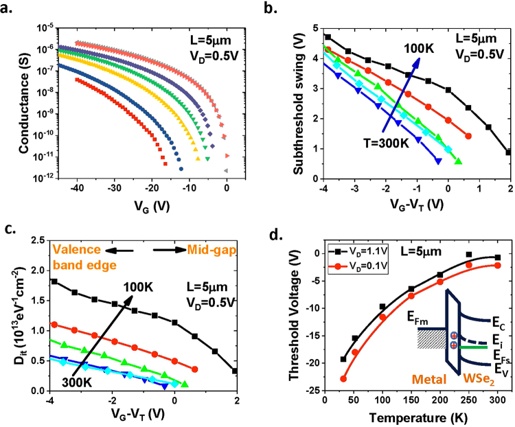
The interface trap density is another key parameter for semiconductors, which directly impacts the performance of metal-oxide field-effect transistors (MOSFETs), tunneling field-effect transistors (TFETs), and tunneling diodes. The interface trap density of the CVD WSe2 is evaluated by measuring the subthreshold swing at various temperatures on the long-channel transistors. Figure 7a shows the ID~VD curves measured at various temperatures for a transistor with gate length L = 5 μm. The subthreshold swing is defined as the gate voltage required to vary the subthreshold current by one decade: , where ID is the drain current at the subthreshold regime. Figure 7b shows the measured subthreshold swing as a function of gate voltage. The subthreshold swing is typically a function of depletion capacitance, CD, and temperature. If there are interface states, an interface-state capacitance, Cit, will be in parallel with the CD. Then the subthreshold swing can be modeled as 36. For transistors with atomically thin channel (monolayer WSe2), it is assumed that the device is fully depleted and CD ≈ 0. Then the interface capacitance, Cit, can be extracted. The interface trap density is related to Cit by the equation , where q is the elementary charge. Figure 7c shows the extracted interface trap density, Dit, as a function of gate overdrive, VG − VT, at various temperatures. As the gate overdrive, VG − VT, decreases, i.e. as the Fermi level at the WSe2/oxide interface approaches the valence band edge, the interface trap density increases, which is similar to the energy distribution of the interface traps in silicon.
Figure 7.
Interface states in back-gated WSe2 transistors. (a) Two-point conductance as a function of gate voltage measured at various temperatures. (b) Subthreshold swing as a function of gate overdrive, VG − VT, at various temperatures. (c) Extracted interface trap density as a function of gate overdrive. (d) Temperature dependence of the threshold voltage. The inset illustrates the positive interface trapped charges located at the WSe2/oxide interface when the gate is biased at the threshold voltage.
The threshold voltages of these back-gated WSe2 transistors are also strongly dependent on the temperatures. Figure 7d shows the threshold voltage as a function of temperature. The threshold voltage increases monotonically as the temperature increases from 35 K to 300 K. This can be explained by the temperature dependence of the interface trapped charges. The interface state typically has two types: the donor-like and the acceptor-like interface states. The donor-like interface states are neutral when filled with electrons and positive when empty, whereas the acceptor-like interface states are negative when filled and neutral when empty. Assuming that the interface states below the midgap Ei are donor-like, while those above Ei are acceptor-like, similar to silicon, the interface states will be positively charged at threshold voltage in p-type transistors, where the Fermi level is below the midgap. This will result in a negative shift in the threshold voltage as compared to the one without interface states. As the temperature increases, the Fermi level is closer to the mid-gap at the threshold voltage, and the total amount of the positive trapped charges reduces, resulting in positive shift of the threshold voltages. The desorption of the moisture from the WSe2 surface as the samples warm up could also cause a threshold voltage shift in these back-gated transistors.
Conclusion
In summary, we have systematically investigated the synthesis of monolayer WSe2 using CVD and studied the electric transport of CVD WSe2. We found that short-channel effect plays an important role in the back-gated WSe2 transistors when the channel length is in the sub-micrometer regime. The drain-induced barrier lowering can result in variations of the threshold voltages and over- or under-estimation of the carrier mobilities. This short-channel effect can also lead to misjudgment of the metal contacts, as the output characteristics of a transistor with ohmic contacts can show Schottky-like behavior. For back-gated WSe2 transistors with 280 nm gate oxide, the DIBL starts to show an upturn when the channel length is shorter than 0.4 µm. This extremely long electrostatic scaling length is due to the thick oxide. These findings will be very important for accurate and unified characterization and analysis of 2D electronic devices with back-gate structures. In addition, we also found that the hydrogen flow rate and the amount of WO3 precursor can significantly influence the morphology of the WSe2. Large work function metal Pd forms ohmic contact to the monolayer WSe2. The interface trap density of WSe2 was extracted from the subthreshold swings. The interface trap density of CVD WSe2 increases as the energy level approaches the valence band edge. These findings will enrich the knowledge of electric transport in CVD WSe2 and the scaled electronic devices based on monolayer TMDCs.
Electronic supplementary material
Acknowledgements
The authors would like to acknowledge the support from NSF ECCS 16-53241 CAR.
Author Contributions
Z.Y. synthesized the WSe2 film by CVD, designed, fabricated and measured the devices. J.L. carried out the AFM measurement and participated the device fabrication. K.X. did the metal evaporation, lift-off, SEM and part of electrical characterization. E.C. carried out the ebeam lithography and metal deposition. W.Z. initiated the project, performed electrical characterization and wrote the manuscript with input from Z.Y.
Competing Interests
The authors declare no competing interests.
Footnotes
Electronic supplementary material
Supplementary information accompanies this paper at 10.1038/s41598-018-23501-4.
Publisher's note: Springer Nature remains neutral with regard to jurisdictional claims in published maps and institutional affiliations.
References
- 1.Jin, Z. H., Li, X. D., Mullen, J. T. & Kim, K. W. Intrinsic transport properties of electrons and holes in monolayer transition-metal dichalcogenides. Physical Review B90 (2014).
- 2.Das, S. & Appenzeller, J. WSe2 field effect transistors with enhanced ambipolar characteristics. Appl Phys Lett103 (2013).
- 3.Chuang HJ, et al. Low-Resistance 2D/2D Ohmic Contacts: A Universal Approach to High-Performance WSe2, MoS2, and MoSe2 Transistors. Nano Letters. 2016;16:1896–1902. doi: 10.1021/acs.nanolett.5b05066. [DOI] [PubMed] [Google Scholar]
- 4.Podzorov V, Gershenson ME, Kloc C, Zeis R, Bucher E. High-mobility field-effect transistors based on transition metal dichalcogenides. Appl Phys Lett. 2004;84:3301–3303. doi: 10.1063/1.1723695. [DOI] [Google Scholar]
- 5.Pradhan NR, et al. Field-Effect Transistors Based on Few-Layered alpha-MoTe2. Acs Nano. 2014;8:5911–5920. doi: 10.1021/nn501013c. [DOI] [PubMed] [Google Scholar]
- 6.Li LK, et al. Black phosphorus field-effect transistors. Nature Nanotechnology. 2014;9:372–377. doi: 10.1038/nnano.2014.35. [DOI] [PubMed] [Google Scholar]
- 7.Xia, F. N., Wang, H. & Jia, Y. C. Rediscovering black phosphorus as an anisotropic layered material for optoelectronics and electronics. Nature Communications5 (2014). [DOI] [PubMed]
- 8.Deng YX, et al. Black Phosphorus-Monolayer MoS2 van der Waals Heterojunction p-n Diode. Acs Nano. 2014;8:8292–8299. doi: 10.1021/nn5027388. [DOI] [PubMed] [Google Scholar]
- 9.Prakash A, Appenzeller J. Bandgap Extraction and Device Analysis of Ionic Liquid Gated WSe2 Schottky Barrier Transistors. Acs Nano. 2017;11:1626–1632. doi: 10.1021/acsnano.6b07360. [DOI] [PubMed] [Google Scholar]
- 10.Agnihotri P, Dhakras P, Lee JU. Bipolar Junction Transistors in Two-Dimensional WSe2 with Large Current and Photocurrent Gains. Nano Letters. 2016;16:4355–4360. doi: 10.1021/acs.nanolett.6b01444. [DOI] [PubMed] [Google Scholar]
- 11.Burg GW, et al. Coherent Interlayer Tunneling and Negative Differential Resistance with High Current Density in Double Bilayer Graphene–WSe2 Heterostructures. Nano Letters. 2017;17:3919–3925. doi: 10.1021/acs.nanolett.7b01505. [DOI] [PubMed] [Google Scholar]
- 12.Wang, J. J. et al. Gate-modulated conductance of few-layer WSe2 field-effect transistors in the subgap regime: Schottky barrier transistor and subgap impurity states. Appl Phys Lett106 (2015).
- 13.Pradhan, N. R. et al. Hall and field-effect mobilities in few layered p-WSe2 field-effect transistors. Sci Rep-Uk5 (2015). [DOI] [PMC free article] [PubMed]
- 14.Das, S., Dubey, M. & Roelofs, A. High gain, low noise, fully complementary logic inverter based on bi-layer WSe2 field effect transistors. Appl Phys Lett105 (2014).
- 15.Chuang H-J, et al. High Mobility WSe2 p- and n-Type Field-Effect Transistors Contacted by Highly Doped Graphene for Low-Resistance Contacts. Nano Letters. 2014;14:3594–3601. doi: 10.1021/nl501275p. [DOI] [PubMed] [Google Scholar]
- 16.Tosun M, et al. High-Gain Inverters Based on WSe2 Complementary Field-Effect Transistors. Acs Nano. 2014;8:4948–4953. doi: 10.1021/nn5009929. [DOI] [PubMed] [Google Scholar]
- 17.Movva HCP, et al. High-Mobility Holes in Dual-Gated WSe2 Field-Effect Transistors. Acs Nano. 2015;9:10402–10410. doi: 10.1021/acsnano.5b04611. [DOI] [PubMed] [Google Scholar]
- 18.Yu L, et al. High-Performance WSe2 Complementary Metal Oxide Semiconductor Technology and Integrated Circuits. Nano Letters. 2015;15:4928–4934. doi: 10.1021/acs.nanolett.5b00668. [DOI] [PubMed] [Google Scholar]
- 19.Kim HJ, Kim DH, Jeong CY, Lee JH, Kwon HI. Determination of Interface and Bulk Trap Densities in High-Mobility p-type WSe2 Thin-Film Transistors. Ieee Electron Device Letters. 2017;38:481–484. doi: 10.1109/LED.2017.2673854. [DOI] [Google Scholar]
- 20.Resta, G. V. et al. Polarity control in WSe2 double-gate transistors. Sci Rep-Uk6 (2016). [DOI] [PMC free article] [PubMed]
- 21.Liu W, et al. Role of Metal Contacts in Designing High-Performance Monolayer n-Type WSe2 Field Effect Transistors. Nano Letters. 2013;13:1983–1990. doi: 10.1021/nl304777e. [DOI] [PubMed] [Google Scholar]
- 22.Xu, S. G. et al. Universal low-temperature Ohmic contacts for quantum transport in transition metal dichalcogenides. 2d Materials3 (2016).
- 23.Liu BL, et al. Chemical Vapor Deposition Growth of Monolayer WSe2 with Tunable Device Characteristics and Growth Mechanism Study. Acs Nano. 2015;9:6119–6127. doi: 10.1021/acsnano.5b01301. [DOI] [PubMed] [Google Scholar]
- 24.Zhou HL, et al. Large Area Growth and Electrical Properties of p-Type WSe2 Atomic Layers. Nano Letters. 2015;15:709–713. doi: 10.1021/nl504256y. [DOI] [PMC free article] [PubMed] [Google Scholar]
- 25.Huang J-K, et al. Large-Area Synthesis of Highly Crystalline WSe2 Monolayers and Device Applications. Acs Nano. 2014;8:923–930. doi: 10.1021/nn405719x. [DOI] [PubMed] [Google Scholar]
- 26.Clark, G. et al. Vapor-transport growth of high optical quality WSe2 monolayers. Apl Materials2 (2014).
- 27.Eichfeld, S. M., Colon, V. O., Nie, Y. F., Cho, K. & Robinson, J. A. Controlling nucleation of monolayer WSe2 during metal-organic chemical vapor deposition growth. 2d Materials3 (2016).
- 28.Eichfeld SM, et al. Highly Scalable, Atomically Thin WSe2 Grown via Metal-Organic Chemical Vapor Deposition. Acs Nano. 2015;9:2080–2087. doi: 10.1021/nn5073286. [DOI] [PubMed] [Google Scholar]
- 29.Wang QH, Kalantar-Zadeh K, Kis A, Coleman JN, Strano MS. Electronics and optoelectronics of two-dimensional transition metal dichalcogenides. Nature Nanotechnology. 2012;7:699–712. doi: 10.1038/nnano.2012.193. [DOI] [PubMed] [Google Scholar]
- 30.Ross JS, et al. Electrically tunable excitonic light-emitting diodes based on monolayer WSe2 p-n junctions. Nature Nanotechnology. 2014;9:268–272. doi: 10.1038/nnano.2014.26. [DOI] [PubMed] [Google Scholar]
- 31.Baugher BWH, Churchill HOH, Yang YF, Jarillo-Herrero P. Optoelectronic devices based on electrically tunable p-n diodes in a monolayer dichalcogenide. Nature Nanotechnology. 2014;9:262–267. doi: 10.1038/nnano.2014.25. [DOI] [PubMed] [Google Scholar]
- 32.Pospischil A, Furchi MM, Mueller T. Solar-energy conversion and light emission in an atomic monolayer p-n diode. Nature Nanotechnology. 2014;9:257–261. doi: 10.1038/nnano.2014.14. [DOI] [PubMed] [Google Scholar]
- 33.Zeng, H. L. et al. Optical signature of symmetry variations and spin-valley coupling in atomically thin tungsten dichalcogenides. Sci Rep-Uk3 (2013). [DOI] [PMC free article] [PubMed]
- 34.Yan RH, Ourmazd A, Lee KF. Scaling the Si Mosfet - from Bulk to Soi to Bulk. IEEE Transactions on Electron Devices. 1992;39:1704–1710. doi: 10.1109/16.141237. [DOI] [Google Scholar]
- 35.Majumdar A, Ren ZB, Koester SJ, Haensch W. Undoped-Body Extremely Thin SOI MOSFETs With Back Gates. IEEE Transactions on Electron Devices. 2009;56:2270–2276. doi: 10.1109/TED.2009.2028057. [DOI] [Google Scholar]
- 36.Hori, T. Gate dielectrics and MOS ULSIs: principles, technologies, and applications. (Springer, 1997).
Associated Data
This section collects any data citations, data availability statements, or supplementary materials included in this article.


