Abstract
The integration of biosensors, microfluidics and CMOS instrumentation provides a compact lab-on-CMOS microsystem well suited for high throughput measurement. This paper describes a new epoxy chip-in-carrier integration process and two planar metallization techniques for lab-on-CMOS that enable on-CMOS electrochemical measurement with multichannel microfluidics. Several design approaches with different fabrication steps and materials were experimentally analyzed to identify an ideal process that can achieve desired capability with high yield and low material and tool cost. On-chip electrochemical measurements of the integrated assembly were performed to verify the functionality of the chip-in-carrier packaging and its capability for microfluidic integration. The newly developed CMOS-compatible epoxy chip-in-carrier process paves the way for full implementation of many lab-on-CMOS applications with CMOS ICs as core electronic instruments.
Keywords: lab-on-CMOS, chip-in-carrier, planar metallization, CMOS biosensor, screen-printing
I. Introduction
OVER past two decades, lab-on-chip technology has greatly advanced to become one of the key technologies in chemical, biological and medical applications including bio-sensing, environmental monitoring, drug discovery and clinical diagnosis [1–3]. Lab-on-chip miniaturizes and integrates one or several laboratory functions on a small size chip to achieve automated microfluidics and high-throughput screening. However, lab-on-chip devices have remained largely passive, without integrated instrumentation electronics that could significantly improve system form factor and provide tremendous benefits like better signal routing capability, better sensitivity, lower noise and lower power consumption. Modern microelectronics allow the functions of bench top instruments to be replaced by custom CMOS IC readout chips. A simple approach is to place a CMOS IC adjacent to the lab-on-chip device. However, unless the core lab-on-chip sensing operation takes place on the immediate surface of a CMOS IC, the important performance benefits associated with reducing the signal path to the micron scale cannot be achieved. A critical challenge in integrating CMOS ICs with lab-on-chip devices is the size mismatch between the two components. Microfluidic devices usually have dimensions in centimeters while CMOS die have dimensions in millimeters. This dimensional mismatch prohibits direct integration of microfluidics and CMOS ICs using conventional approaches.
CMOS readout chips have been reported for on-CMOS sensing in liquids without microfluidics [4–11], where the functionality of fluid handling was rudimentary. Due to structural constraints imposed by bonding wires and package frames for CMOS packaging, these devices were incapable of implementing even basic microfluidic capabilities such as mixing or pumping. To address this deficiency, our group recently introduced the “lab-on-CMOS” concept to realize multichannel lab-on-chip functions with sensing on the surface of a CMOS chip [12]. The lab-on-CMOS platform can be defined as a microsystem where a wide variety of lab-on-chip functions are combined with multichannel sensing on the surface of a CMOS readout chip that minimizes signal routing to improve noise performance and sensitivity. In this initial lab-on-CMOS design, CMOS ICs were embedded in holes etched into a silicon carrier that expanded surface area for lab-on-chip integration. However, the fabrication and assembly processes for this silicon chip-in-carrier assembly are complex, low yield and labor intensive. In contrast, similar chip-in-carrier structures have been implemented using epoxy in processes called reconstructed wafer, wafer level embedding technology and molded reconfigured wafer [13–17]. Unfortunately, these processes need expensive packaging tools and/or highly specialized, often proprietary, polymer materials. Another polymer carrier was reported with low cost single die microfluidic integration but requires skilled manual manipulation in a key step [18].
To address the shortcomings in existing processes to integrate lab-on-chip functionality on top of CMOS readout chips, this paper presents new methods to realize an epoxy chip-in-carrier assembly that is reliable while using lower cost materials and processes. Expanding on prior preliminary results [19, 20], this paper provides a comprehensive analysis of the new epoxy packaging process with experimental iterations that progressively explore optimal chip-in-carrier solutions. In addition, this paper introduces a reliable screen-printed silver ink metallization option to traditional thin film metal interconnects and presents new results from electrochemical and microfluidic experiments. Lab-on-CMOS technologies are still in their infancy, and this work discusses and demonstrates several new approaches that may inform and inspire future innovations. In Section II, CMOS packaging options for liquid environment sensing will be reviewed. In Section III, the development of chip-in-carrier integration process will be described, and techniques for realizing interconnects on the carrier will be presented in Section IV. Section V will report experimental results followed by conclusions in Section VI.
II. Lab-on-Cmos: Requirements and Technologies
One of the major challenges in lab-on-CMOS integration is that lab-on-chip microfluidic structures occupy large surface areas compared to those of CMOS die. Practically, the area of a CMOS die is not increased to the scale of centimeters because of manufacturing cost. Alternatively, the area of the CMOS chip could be expanded with the help of a carrier to support microfluidic functions. The carrier must also support electrical connections enabling the CMOS chip to function as an electronic interface between on-CMOS sensors and the external world. The carrier integration and packaging scheme must meet several other requirements, including: 1) physically isolating the fluids from electrical I/O signals; 2) sealing microfluidics on top of CMOS chip or carrier; and 3) using packaging and fabrication methods compatible with the integrated circuits. The combination of multichannel microfluidics and on-CMOS sensor arrays provides a new platform for high throughput applications that take advantage of massively parallel sensing structures. For example, an on-CMOS multichannel microfluidic serial dilution scheme that allows measurement of multiple sample concentrations has been demonstrated [21]. Here, the challenges of complex microfluidic structures are addressed outside the CMOS chip surface, thus reducing design and integration complexity while still enabling key sensing activities to be realized on CMOS.
A. Chip-in-Carrier Integration: Silicon or Epoxy
To support CMOS integration with microfluidics, chip-in-carrier approaches using silicon or epoxy carriers have been reported [14–19, 22, 23]. Silicon carrier fabrication relies on established semiconductor processing tools, and one of the key procedures is the deep reactive ion etching (DRIE) of a silicon wafer to create the holes in a silicon substrate. The CMOS chip is embedded in the hole with polymer or spin-on-glass sealing the gap. The hole size and shape should match the chip as closely as possible in order to minimize the use of sealant. However, CMOS chips are manufactured by dicing a large wafer, and the size of individual chips can easily vary by tens of micrometers. Therefore, it is not practical to make a universal photomask for DRIE silicon etching to fabricate the holes in the silicon carrier. The DRIE process is also expensive and not available in all manufacturing facilities. For a wafer level carrier process where a large carrier area is needed, however, a silicon carrier is desirable because it does not produce much stress with minimal use of polymer filler. On the other hand, an epoxy carrier is made by molding epoxy around the CMOS chip so that the carrier will automatically align to the chip. This process does not require lengthy photolithography and silicon etching process and thus can be produced at low cost. The epoxy material should possess thermal and chemical properties that allow the subsequent integration steps. For a single CMOS die, mismatch in the coefficient of thermal expansion (CTE) between the epoxy carrier and the silicon die as well as deformation of the epoxy carrier have not been observed to be significant issues. However, if a wafer-scale carrier is desired, the CTE mismatch for epoxy carriers could become problematic and necessitate the complexity and cost of a silicon carrier.
For both silicon and epoxy carriers, a temporary handling wafer is used to hold the CMOS chip while the carrier is installed (silicon) or molded (epoxy) around the chip. A temporary bonding of the handling wafer is required because bonding should be maintained throughout the chip-in-carrier assembly process but the handling wafer must be detached after the assembly is completed.
B. Interconnects
The main techniques used to form interconnections with CMOS chips are tape automated bonding (TAB) [24], wire bonding, and flip-chip. TAB is not ideal for lab-on-CMOS applications because of temperature restrictions and incompatibility with integration of microfluidic channels. Several groups have reported integration platforms based on wire bonding interconnections [10, 11]. One apparent shortcoming of metal wire bonds is the difficulty in protecting them from the chemical corrosion and electrical short circuit. Moreover, bonding wires significantly impede integration with microfluidics. In the flip-chip method, the active surface of the CMOS chip is attached to a bonding substrate, and interconnections between the CMOS I/O pads and package pins are realized by solder bumps through thermal heating or thermosonic bonding [9, 25, 2 ]. However, the bonding substrate blocks the CMOS chip surface and makes it impossible or at least very complex to implement on-CMOS sensors or on-CMOS microfluidics. Moreover, the flip-chip method requires specific CMOS bonding pad design and various extra materials and processes that add cost and complexity, including underfill epoxy, substrate metallization, substrate solder mask and chip passivation.
Alternatively, planar thin film metal deposition has been widely used in microfabrication to make contacts and form electrical routings. By precise photolithography, metal interconnections could be well defined and the small thickness of the metal film imposes little restriction to microfluidic integration. Similarly, planar metal interconnect formed using conductive inks can also be used to fabricate electrical routings. With larger thickness compared to thin film metals, conductive inks form more reliable interconnects but make it harder to fabricate precise routing patterns.
III. Epoxy Chip-in-Carrier Integration
Based on the analysis in Section II, an epoxy carrier and planar metal interconnection were adopted for the single die chip-in-carrier process described by this paper. Fig. 1 illustrated the conceptual view of a lab-on-CMOS microsystem based on these chosen chip-in-carrier process options. Here, sensors are directly fabricated on the surface of a CMOS chip that is embedded into an epoxy carrier. Signals are routed off the CMOS chip and onto the carrier using planar metal interconnects across the surface of the integrated platform. The planar metallization allows for subsequent formation of complex microfluidics directly on top of the CMOS chip and surrounding carrier. Multichannel microfluidics is bonded atop the expanded surface area of the chip-in-carrier assembly. Although the CMOS chip could have embedded readout circuits and an array of sensors on its surface, this paper will focus on the physical integration processes of the Fig. 1 concept model and not on electronics or sensing issues and performance.
Fig. 1.
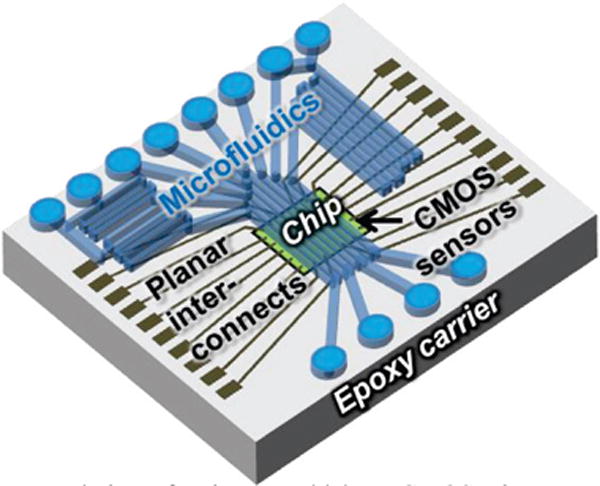
Conceptual view of an integrated lab-on-CMOS microsystem.
A. Overview
The general fabrication procedure for the epoxy chip-in-carrier integration is shown in Fig. 2. First, the chip is attached via a temporary bonding layer to a glass holder with the chip’s top surface facing the holder as shown in Fig. 2(a). The bonding should be temporary in order to release the chip and the epoxy carrier later. Second, another glass holder is placed and pressed on top of the chip and epoxy is filled into the gap between the two glass holders as shown in Fig. 2(b). Third, the liquid phase epoxy is then cured and the temporary bonding layer is dissolved to remove the bottom glass holder, as shown in Fig. 2(c). The top surfaces of epoxy carrier and chip should be flat. Similar procedures were reported in the past [16, 23], but key information of the process, such as the temporary bonding material, composition of proprietary epoxy and die handling tools, were not reported and the work could not be repeated. Therefore, experimental development of the epoxy chip-in-carrier process was necessary to establish the design details for this approach.
Fig. 2.
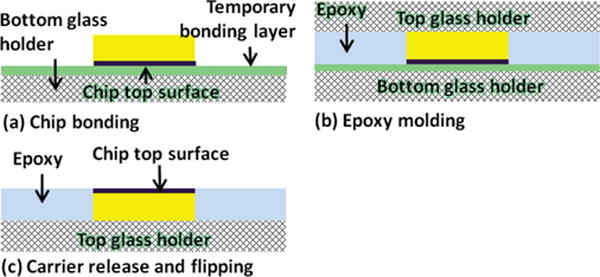
Process flow of epoxy chip-in-carrier integration. (a) The chip is temporarily bonded to a glass holder with top surface facing the glass holder. (b) Top glass holder covers and presses on the top of the chip and the epoxy is filled into the gap and cured. (c) The temporary bonding layer is etched or dissolved and the bottom glass holder is released, after which the epoxy carrier and chip surfaces are flush.
The main purpose of the epoxy in this work is to form the chip carrier by molding around the chip. As the most used structural material in MEMS microfabrication, SU-8, a negative photoresist, was considered first. Typically, SU8 is soft baked to evaporate solvents before going through UV exposure. In our process, with the presence of the glass holders, the SU8 solvent could not properly evaporate during soft bake. Thus, the baking time had to be greatly increased, but this made the SU8 almost impossible to get ready for the upcoming UV exposure. Due to this drawback of SU8, it was not chosen for the carrier material. Instead of SU8, a thermally cured epoxy was selected due to its simple curing method. This epoxy can be cured without baking at room temperature, or baking at higher temperature could be employed for faster curing. Different types of epoxy are bio-compatible and available in various viscosities and glass transition temperatures to work in different conditions.
B. Chip-in-Carrier Process
The temporary bonding layer in Fig. 2 must adhere to several important requirements. The temporary bonding material should be immiscible with epoxy and should be dissolvable after the epoxy is cured. The bonding should be tight enough preventing epoxy smear under the chip. The liquid temporary bonding material should be as thin as possible so that carrier and chip surfaces stay flush.
Photoresist was the first material considered for the temporary bonding layer. It is often used as a sacrificial material for the lift-off process and as an adhesive layer that can be dissolved by acetone or photoresist stripper. Unfortunately, in our experiments photoresist was found to mix with epoxy during the molding step. To address this issue, a parylene coating was applied after the chip was bonded to serve as an intermediate layer. Parylene is a polymer material that can be deposited at room temperature with a uniform coverage on all exposed surfaces. Parylene is also a good electrical insulator and is resistive to chemical corrosion.
The process flow for the photoresist-parylene bonding layer is described in Fig. 3-I. First, photoresist was spin coated at 3000rpm on the glass holder and the chip was bonded to the glass holder with its top surface facing toward the glass holder, as shown in Fig. 3-I(a). The photoresist was baked on a hotplate at 110°C to bond the chip while the chip was pressed uniformly to avoid a weak bonding point. Second, a thin 5μm parylene film was deposited on the chip using room temperature vapor deposition as shown in Fig. 3-I(b). Then, another glass holder was placed on top of the chip, parallel to the bottom glass holder. Epoxy resin was then dispensed into the gap between the two glass holders to form the carrier. The epoxy was supplied at one end of the gap between glass holders and was observed to travel forward through the gap to the opposite end by capillary effect. This process is further illustrated in Fig. 4. Because the epoxy filled the gap as the meniscus traveled from one side to the opposite side, this process minimized trapped bubbles inside the epoxy carrier. After the epoxy was cured at room temperature, the epoxy carrier was ready for release. The whole structure was immersed in acetone bath to dissolve the photoresist and cleaned by DI water as shown in Fig. 3-I(c) and 3-I(d).
Fig. 3.
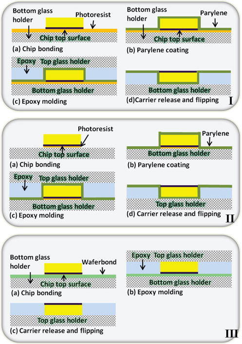
Process flows for three different epoxy chip-in-carrier integration methods with different materials and steps. I: chip-in-carrier process with photoresist as a temporary bonding layer; II: modified chip-in-carrier process with photoresist as a temporary bonding layer that is present only beneath the chip; III: chip-in-carrier process with Waferbond as a temporary bonding layer.
Fig. 4.
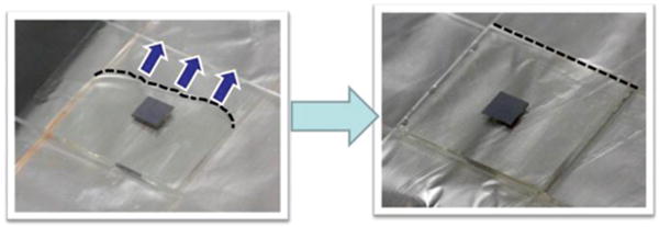
Top view of the silicon chip sandwiched by the two glass holders while the epoxy is filled between the two 1” × 3” glass slides from one side and the epoxy meniscus (dotted line) travels through the gap by capillary force (left) until completely filling the overlapping area (right).
Initially, Shipley 1813, a thin positive photoresist, was selected as the bonding layer photoreisist. Shipley 1813 was spin coated as thin as ~1μm. However, after the epoxy was molded and cured, the area to release was too large, 1” × 1” in this case. Consequently, AZ4620, a photoresist that can be applied as thick as 8μm, was spin coated on the glass holder to have a thicker release layer. The rest of the process steps were exactly the same as those in Fig. 3-I. With the thicker photoresist, the epoxy carrier was successfully released in the acetone bath. Along the chip-to-carrier boundary a discontinuous surface profile was observed and the surface transition was often found to be very abrupt. This deep gap is highly undesired because it can cause difficulty in routing surface metals to continuously cross the chip-carrier boundary. This problem is caused by the push-out effect of the adhesives at the bonding interface, as shown in Fig. 5. The push-out photoresist occupies the space, stopping the epoxy from molding seamlessly around the chip and creating valley between the chip and the carrier. The thicker and the more fluid the photoresist adhesion layer is, the more the photoresist is pushed out. Therefore, thick AZ4620 produced more push-out effect than thin Shipley 1813. The push-out effect of AZ4620 was verified by inspecting the bonded chip under scanning electron microscope (SEM). In the SEM image as shown in Fig. 5, the AZ4620 adhesion layer can be seen to be pushed out around the chip edges and accumulated on the sidewall of the chip.
Fig. 5.
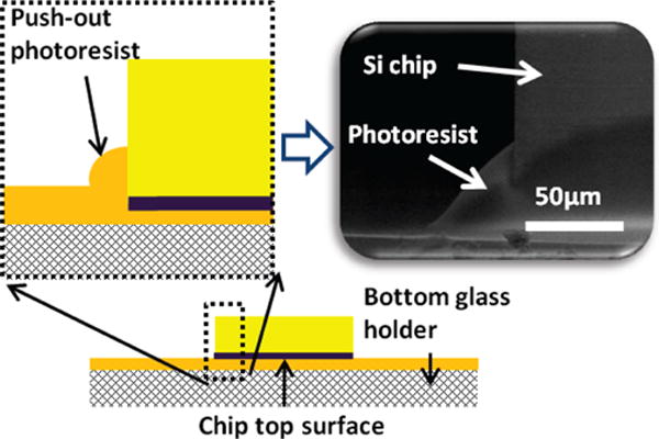
Push-out effect at the bonding interface between the silicon chip and the photoresist adhesive film.
To address the shortfalls of both thin and thick photoresists as a temporary bonding layer, a new process was designed. As shown in Fig. 3-II, the new method used thin photoresist to minimize the push-out effect but limits the area coated by photoresist to only beneath the chip. Using a process flow similar to the previous ones, the chip was bonded to the holder using thin AZ5214 photoresist that was subsequently exposed (using the chip as a physical mask) and developed. This leaves photoresist only under the chip, as shown in Fig. 3-II(a), ensuring only the photoresist area necessary for bonding is used. A layer of 5μm parylene was then coated over the chip and glass holder, as shown in Fig. 3-II(b). Then, epoxy was injected into the gap between the holders and cured as described previously, as shown in Fig. 3-II(c). The bottom glass holder was then removed by peeling it off the parylene layer, which has weak adhesion to glass without any surface treatment. Once the bottom glass holder was removed, the structure was then immersed in acetone to dissolve the photoresist on the chip surface, resulting in the structure shown in Fig. 3-II(d). As desired, this process resulted in a much improved (smaller) gap size. However, although the bottom holder was easily peeled from parylene along the epoxy areas, it did not cleanly release around the adhesive thin photoresist film and created some rough edges around the chip-carrier boundary, which is a critical region for subsequent formation of metal interconnects from chip to carrier. Several steps were explored to remove or circumvent the rough parylene edges, including plasma etching and formation of a planarization layer. While these steps were shown to resolve the problem, they added significant complexity to the process and motivated discovery of a more effective temporary bonding method.
The experimental design efforts above illuminated the fact that the temporary bonding material plays a critical role in producing a smooth surface transition between chip and carrier. To avoid the problems associated with photoresist, we next explored the use of Waferbond (Brewers Science, Inc. USA), a specially designed temporary bonding material. Waferbond was developed for die and thin wafer handling and has a well-defined bonding characteristics. It is a low-viscosity solvent that forms 10 to 27μm coatings that are resistant to acids, bases, and most solvents. Moreover, Waferbond does not mix with epoxy and allows molding epoxy without an intermediate layer like parylene.
Building on the previously presented process of Fig. 3-II, a new process was developed using Waferbond as the temporary bonding material. As shown in Fig. 3-III, the first step was chip bonding, where the chip was gently placed on the 10μm Waferbond coating without pressure, followed by baking on hotplate at 180°C for 2 minutes. To release the bottom holder after epoxy carrier formation, the Waferbond was dissolved in a Waferbond remover bath at 110°C for 2 hours and then rinsed off at 70°C for 15 minutes. This method was shown to provide a simple process flow that produced a smooth chip-carrier surface. Thus, the Waferbond-based chip-in-carrier packaging method (Fig. 3-III) was utilized for the subsequent integrated device development reported below. However, the photoresist-based methods were also functional and were discussed here because they may be preferred for different applications.
IV. Interconnects
After releasing the bottom holder, surface profile measurements show that the difference between chip and carrier heights is typically only about 3μm, but the gap width and depth between the chip and carrier can be greater than 20μm due to push-out effect. This discontinuity must be considered during fabrication of metal interconnect that route signals between the carrier edge and chip I/O pads. Thin film metal deposition is the most common way to form microfabricated interconnects, and thin film metals typically must be less than 1μm thick to remain cost effective. Therefore, to ensure a smooth transition across the chip-to- carrier boundary, a surface planarization step was employed before metallization.
A. Thin Film Metal Interconnects
Starting with a chip-carrier assembly based on the Fig. 3-III Wafterbond process, a 10μm layer of SU8 was spin coated and patterned on the chip-carrier assembly. As illustrated in Fig. 6(a), this alleviated the discontinuity at the chip-carrier boundary, allowing continuous coverage of thin film metal across the boundary. A 50Å/8000Å Ti/Cu thin film layer was then deposited by physical vapor deposition (PVD) and patterned to form interconnects between chip bond pads and carrier edge contacts, as shown in Fig. 6(b). To insulate the interconnects in preparation for addition of a microfluidic layer, a 5μm parylene layer was then deposited over the chip-carrier assembly. Parylene was then patterned in O2 RIE (reactive ion etching) to expose only the on-CMOS sensing electrode areas.
Fig. 6.

Thin film interconnect process flow: (a) planarization layer to bridge carrier and chip; (b) metal interconnects deposited and patterned.
During experimental development of this thin film deposition process, a tradeoff was observed between the thickness of the planarization layer that would effectively resolve chip-carrier discontinuities and the yield of the thin film interconnects. Thicker planarization layers more reliably covered the discontinuity but required thicker thin film metals to reliably cover the step at the edge of the planarization layer (see Fig. 6(b)). PVD metal deposition becomes expensive for thick layers and is generally limited to only 1~2μm. Furthermore, thin film metal interconnects are vulnerable to unexpected irregular surface profiles or scratches that lower the yield. For these reasons, a new interconnect formation process was explored that could provide high yield and reliability at low fabrication cost.
B. Silver Ink Interconnects
Screen printing is a well-developed technology in which ink or resin is deposited over a substrate through a predefined mask or “screen.” Using conductive ink, screen-printed planar metallization can deposit layers thick enough to overcome uneven surface profiles. Additionally, compared to thin film deposition, screen-printing offers a wide material selection and low process cost. Traditional screen printing methods use mesh screens together with blocking stencils or photo emulsion. The thickness of the mesh wire determines the minimum feature sizes that can be printed, which is generally greater than 100μm. Comparing screen printing to the lift-off photolithography method used in microfabrication, we see many similarities, where lift-off photolithography typically uses photoresist and thick films in place of screen printing’s mesh screen and conductive ink. Combining the two, we developed a CMOS compatible silver ink interconnect process for chip-in-carrier planar metallization that uses photoresist as sacrificial screen that can be patterned at high resolution. Important considerations in developing this process are that the ink solvent must be immiscible with photoresist and any excessive ink remaining after printing must be removable with photoresist lift-off after the ink is cured.
Fig. 7 illustrates the CMOS-compatible modified screen printing process that was developed. First, the chip was prepared by depositing thin film gold (Au) on the surface and patterning to cover only bond pads and sensing electrodes. Then the epoxy carrier was produced and the bottom holder was released using methods described above, and the resulting chip-in-carrier assembly is shown in Fig. 7(a). The first step of the interconnect process was to deposit a 10μm parylene layer (parylene1) over the entire chip-in-carrier assembly. This parylene layer provides some planarization and, most importantly, insulates the chip, especially any exposed silicon on the chip’s edge. The parylene1 layer is then patterned by O2 RIE to cover the carrier and chip-carrier boundary and expose everything inside the chip bond pads. Next, AZ4620 photoresist was spin coated at 2000rpm over the assembly to form a sacrificial mask for metallization that is thick enough to continuously cover steps at the chip-carrier boundary. The photoresist was then exposed by UV light and developed to form a lift-off mask for planar interconnect formation. Conductive ink was then dispensed with pipette through the AZ4620 mask and a flat elastic squeegee was used to sweep along the mask surface to remove excess conductive ink. Silver (Ag) nanoparticle ink, PG-007 (Paru Co), was selected for the screen-printed interconnects because of its high conductivity and flexible viscosity. Also, the solvent in PG-007 is immiscible with AZ4620 and will not harm the photoresist mask. The whole assembly was then baked at 9°C for 1 hour using a hotplate to cure the silver ink. After silver ink was cured, acetone and DI water were used to lift off the AZ4620 mask, remove any excess silver ink and reveal the interconnect patterns. This metallization process provided an approximately 10μm planar interconnects layer, which was thick enough to form continuous conductive paths that overcome all discontinuities between the CMOS die and the carrier. To prepare for subsequent addition of a microfluidic layer, a second parylene layer (parylene2 in Fig. 7(c)) was then deposited at 5μm and patterned by O2 RIE process. The parylene2 layer insulates the interconnects from the aqueous environment, exposing only the on-chip sensing electrodes.
Fig. 7.
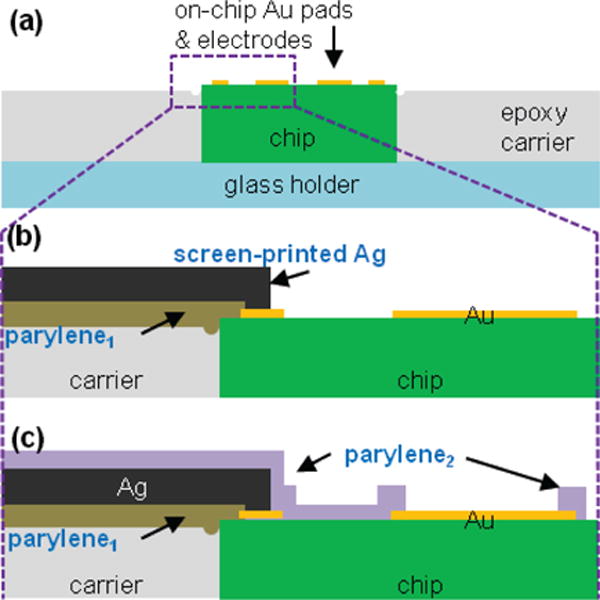
Post-CMOS process flow for chip-in-carrier approach with screen printed planar interconnects: (a) device after epoxy chip-in-carrier process using a dummy dielectric-coated Si die to mimic a CMOS chip; (b) first parylene coating to cover die edge followed by Ag planar electrical interconnects screen-printed on surface of the chip-in-carrier assembly; (c) second parylene layer to insulation all but sensor electrodes from the aqueous chemical environment. Following these steps, a microfluidics layer can be attached to the surface.
V. Results
To experimentally characterize the chip-in-carrier packaging and metallization processes described above, mock CMOS die were created by dicing 5mm × 5mm chips from a 4” oxidized silicon wafer. Smaller chips could make CMOS electrode patterning more complicated due to the edge bead effect, but chips as small as 1.5mm×1.5mm have been successfully patterned [27]. To enable electrochemical sensing, 260μm I/O pads and a 2×2 array of 1mm gold electrode cells were formed on the mock CMOS chips by depositing 50Å/1000Å titanium/gold thin films via physical vapor deposition and patterning by photolithography. A biocompatible epoxy EPO-TEK 302-3M (Epoxy Technology, Inc.) was selected for the carrier because of its low viscosity that aids in filling the narrow gap between two glass holders. Chip-in-carrier assembly planar interconnects were fabricated using both thin film and silver ink methods described in Section IV.
A. Interconnects
The chip-in-carrier assembly with thin film metal interconnections is shown in Fig. 8. The chip-in-carrier was fabricated using the method in Fig. 3-II. The chip is embedded in a transparent epoxy carrier, and the copper interconnects run from the carrier surface onto the chip and make electrical connections to the gold chip pads. A close-up view of the chip-carrier boundary region in Fig. 9 shows copper interconnects crossing the boundary from the carrier surface, to the SU8 planarization edge and then making contact to gold pads. The resistance of the copper interconnects was measured to verify the functionality of the packaging and smooth transition between carrier and chip. From individual interconnect measurements shown in Fig. 10, the average Sheet resistance was calculated to be 0.83Ω/sq with standard deviation of 0.41Ω/sq, which was similar to the 0.38Ω/sq sheet resistance of a planar copper trace running only on the carrier surface. These results confirmed that the transition between carrier and chip was smooth enough and did not produce significant resistance for interconnects.
Fig. 8.
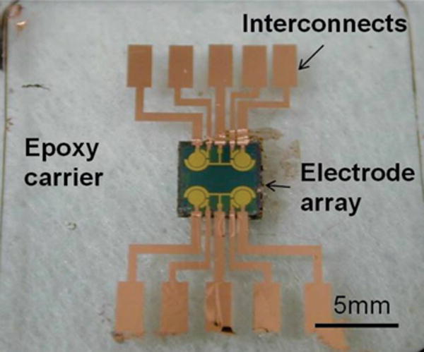
Chip-in-carrier device with thin film metal interconnects and 2×2 electrode array.
Fig. 9.
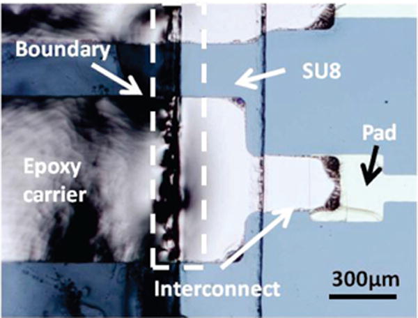
Close-up view of the boundary area between carrier and the chip.
Fig. 10.
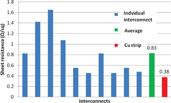
Sheet resistances of individual copper thin film interconnects and their average of 0.83Ω/sq with comparison to a copper strip at 0.38 Ω/sq, with standard deviation of 0.41Ω/sq. The resistance was measured directly across the boundary between the carrier and the silicon die.
Another chip-in-carrier assembly was fabricated using method III in Fig. 3 and metalized using the silver ink process. Optical images of the fabricated device after screen-printed planar metallization are shown in Fig. 11, where all of the layers from Fig. 7 are labeled. For further inspection, the optical and SEM images in Fig. 12 show that the chip-to-carrier discontinuity was completely filled by the screen-printed metallization layer, with no observable breaks in interconnect traces. In our experiment, the interconnects on the carrier were 0.67mm wide. Based on our 10 μm thick photoresist, the screen-printed interconnects can achieve a width as low 30μm and a pitch of around 60 μm limited by the peripheral residual metal fringing seen in Fig. 12. To verify electrical interconnection between the on-chip Au electrodes and the carrier connection pads, resistance of all Ag ink interconnects was measured using a probe station and digital voltage meter. The traces showed average sheet resistance of 1.39Ω/sq with standard deviation of 0.76Ω/sq, which is slightly higher than the resistance of thin film metal traces, mainly because of the higher resistivity of conductive ink compared to elemental copper. The measurement results demonstrated that the new photoresist-based screen printing planar metallization process can reliably form electrical interconnects for lab-on-CMOS platforms.
Fig. 11.
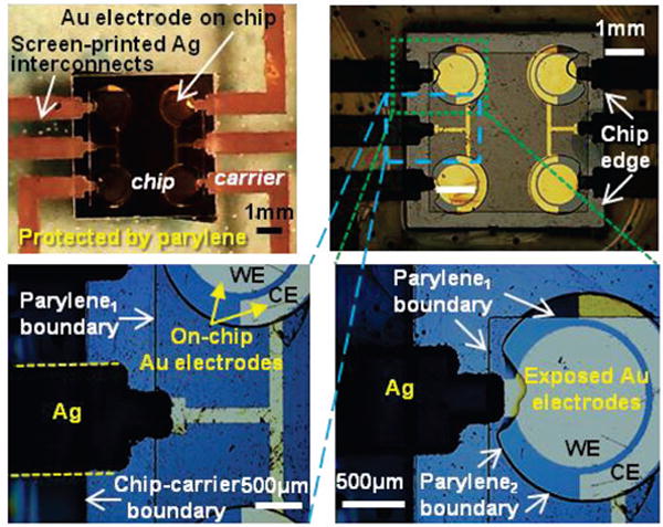
Optical inspection of the screen-printed planar interconnects. Screen printed Ag interconnects were observed to be continuous even when crossing the chip-carrier boundary.
Fig. 12.
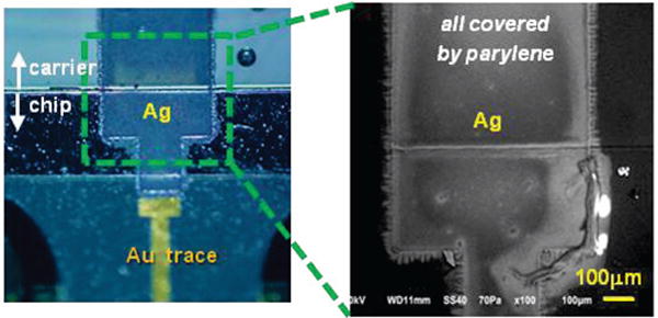
Optical and SEM inspections of the planar Ag ink interconnect protected by a parylene insulation layer.
With limited number of sample sizes, yield of the device is hard to evaluate. In our experiments, the chip-in-carrier device fabricated using the method in Fig. 3-III had a yield of ~80% and both thin film and screen-printed interconnects had a yield of ~100%. In a manufacturing environment with automated equipments and materials, the yield could be further improved. Although, we did not test the temperature range of the device, for the use above room temperature, theoretically the epoxy glass transition temperature of 55°C could be the limiting factor of the whole system.
B. Electrochemical Measurements
The chip-in-carrier with thin film metal interconnects was evaluated for electrochemical sensing. A parylene passivation layer was deposited and patterned to insulate the Cu wires and expose only the gold electrodes. A commercial instrument (CHI760C, CH Instruments Inc.) was used to perform cyclic voltammetry (CV) measurements using a typical electrolyte solution with 0.1M potassium chloride and 1mM potassium ferricyanide (K3[Fe(CN)6]). A reservoir was fabricated using Sylgard 184 PDMS polymer and bonded on the carrier to hold the electrolyte solution. On-chip WE and off-chip commercial liquid junction Ag/AgCl RE and a platinum CE were used. 10 cycles of the resulting redox cycling plot is shown in Fig. 13 with clear redox current peaks. These results confirm that the on-chip gold WE remained clean and unaffected after going through the chip-in-carrier fabrication process. The parylene insulation was also observed to be intact to protect the interconnects.
Fig. 13.

Cyclic voltammetry measurement of 1mM potassium ferricyanide solution with the gold working electrodes on the chip with thin film metal interconnects. Off chip RE and CE were used.
For the chip-in-carrier with silver ink interconnects, a similar CV measurement was performed between 0V - 0.5V with scan rate of 100mV/s for potassium ferrocyanide (K4[Fe(CN)6]) using an on-chip gold WE and off-chip RE and CE. In this experiment, the concentration of K4[Fe(CN)6] was varied and different reduction and oxidation peak currents were collected, as shown in Fig. 14. Again, the result demonstrated both the electrochemical functionality of the gold working electrode after going through fabrication processes and the intactness of the passivation layer over the chip-in carrier interconnects.
Fig. 14.
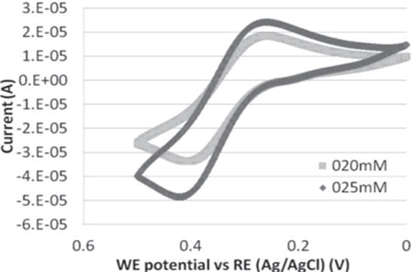
Cyclic voltammetry measurements of 20mM and 25mM potassium ferrocyanide solutions with the gold working electrodes on the chip-in-carrier with silver ink interconnects in microfluidics. Fluid was pumped in through a PDMS channel, and off chip RE and CE were used.
C. Microfluidic Leakage Test
To demonstrate the microfluidic capability of epoxy chip-in-carrier for lab-on-CMOS applications, a PDMS multichannel microfluidic structure was prepared. An SU8 mold was fabricated on a silicon wafer and 10:1 ratio mixed polymer of Sylgard 184 PDMS and curing agent was poured over the SU8 mold and cured overnight at room temperature. The cured PDMS structure was precisely aligned with assistance of mask aligner and bonded onto the chip-in-carrier assembly with uncured PDMS as adhesive. The chip-in-carrier with silver ink interconnects was used to test microfluidic integration, as shown in Fig. 15. With a syringe pump, fluid with blue dye was slowly flowed through the microchannel to test if the thick metallization layer created any leakage paths beneath the fluidics. Fig. 15(a) shows that the device allows fluid to flow across a series of screen-printed metal interconnects on the carrier, and Fig. 15(b) shows that the device allows fluid to flow from carrier, onto chip, and back onto carrier. No leakage was observed at the steps on the device surface at these low-pressure operations during any of these experiments, demonstrating that the epoxy chip-in-carrier is suitable for lab-on-CMOS applications, where the expanded surface area permits use of a wide range of microfluidic structures. For a high pressure microfluidic operation, the microfluidic bonding can be improved through molding the microfluidic PDMS structure directly on the device [28].
Fig. 15.
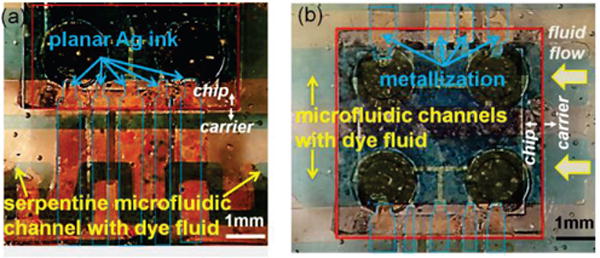
No-leakage test: After the integration with PDMS microchannel, the system was tested with dyed DI water driven by syringe pump. (a) the fluid passes over multiple planar metallization traces; (b) the fluid flows across the chip-carrier boundary and over Au electrodes on the silicon chip.
To help evaluate the packaging and interconnection technologies that have been reported for lab-on-CMOS applications, Tables I and II provide a qualitative assessment of their relative complexity and list some drawbacks and merits of each approach. This paper has highlighted design considerations and results for epoxy carriers and both thin film and screen printed metal interconnects, which we feel are the best approaches reported to date for the strict purpose of combining on-CMOS sensing and microfluidic operation.
TABLE I.
Summary of lab-on-CMOS packaging approaches
| Technique | Complexity | Potential drawback | Merits | Ref. |
|---|---|---|---|---|
| Silicon carrier | High | Expensive process; low yield; labor intensive; lime consuming. | Physically rigid; minimum CTE mismatch. | [17], [21] |
| Epoxy carrier | Moderate | Time consuming. | Low material and tool cost; good for microfluidic integration; polymer molding. | [14–16, [18, 19], [22] |
| Constrained package* | Low | Not suitable for microfluidic integration. | Simple process and suitable for reservoir structure application. | [4–11] |
packages constrained by bonding wires or package frame
TABLE II.
Summary of lab-on-CMOS metal interconnect approaches
| Technique | Complexity | Potential drawback | Merits | Metal thickness | Ref. |
|---|---|---|---|---|---|
| Wire bonding | Low | Significantly impede microfluidic integration; difficult to protect wires. | High yield; high density. | 75 μm | [10, 11] |
| Flip chip | High | Non-smooth surface; impede microfluidic integration; expensive tool cost. | Suitable for 3D chip stacking. | 120 μm* | [9], [24, 25] |
| Tape automated bonding | High | Non-smooth surface; impede microfluidic integration; high temperature. | Suitable for flexible electronics development. | 50–100 μm | [23] |
| Thin film metal | Moderate | Low yield covering surface steps due to thin film thickness (1μm max). | Smallest feature size, flexible pattern design; low cost. | 100 nm | [18, 19], [21] |
| Screen-printing | Moderate | Resolution restrict, interconnect pitch > 50 μm. | Flexible pattern design; low cost. | 10 μm | [20] |
includes height of the PCB, copper traces, and solder bumps
It is important to note that this chip-in-carrier approach is not only limited to lab-on-CMOS applications but can be used in any integration situations where extending the surface of a chip is desired to interface with other devices. This chip-in-carrier packaging scheme provides a universal platform for many highly integrated multi-component, multi-function smart microsystems that possess a CMOS IC as the core measurement or processing element.
VI. Conclusion
To realize lab-on-CMOS integration, a new epoxy-based chip-in-carrier packaging scheme with both thin film and silver ink interconnects was presented. Comprehensive analysis of the fabrication procedures, materials and process complexity were discussed to determine optimal packaging solutions. The chip-in-carrier packaging was evaluated using by interconnect resistance measurements, electrochemical and microfluidic experiments. The results show that the chip-in-carrier packaging can be highly effective for lab-on-CMOS applications.
Acknowledgments
This work was supported by the National Science Foundation under grant ECCS-1307939 and National Institutes of Health under grant R01ES022302.
References
- 1.Wang J. Amperometric biosensors for clinical and therapeutic drug monitoring: a review. Journal of Pharmaceutical and Biomedical Analysis. 1999;19(1–2):47–53. doi: 10.1016/s0731-7085(98)00056-9. [DOI] [PubMed] [Google Scholar]
- 2.Rogers K. Biosensors for environmental monitoring: a regulatory perspective. TrAC Trends in Analytical Chemistry. 1995;14(7):289–294. [Google Scholar]
- 3.Keusgen M. Biosensors: new approaches in drug discovery. Naturwissenschaften. 2002;89(19):433–444. doi: 10.1007/s00114-002-0358-3. [DOI] [PubMed] [Google Scholar]
- 4.Frey U, Sedivy J, Heer F, Pedron R, Ballini M, Mueller J, Bakkum D, Hafizovic S, Faraci FD, Greve F, Kirstein KU, Hierlemann A. Switch-matrix-based high-density microelectrode array in CMOS technology. IEEE J Solid-State Circuits. 2010;45(2):467–482. [Google Scholar]
- 5.Ghafar-Zadeh E, Sawan M, Therriault D. Novel direct-write CMOS-based laboratory-on-chip: design, assembly and experimental results. Sensors and Actuators A: Phys. 2007;134(1):27–36. [Google Scholar]
- 6.Christen JMB, Andreou AG. Design, fabrication, and testing of a hybrid CMOS/PDMS microsystem for cell culture and incubation. IEEE Trans Biomed Circ Syst. 2007;1(1):3–18. doi: 10.1109/TBCAS.2007.893189. [DOI] [PubMed] [Google Scholar]
- 7.Hwang S, Lafratta C, Agarwal V, Yu X, Walt D, Sonkusale S. CMOS microelectrode array for electrochemical Lab-on-a-Chip applications. IEEE J Sensors. 2009;9(6):609–615. [Google Scholar]
- 8.Prodromakis T, Michelakis K, Zoumpoulidis T, Dekker R, Toumazou C. IEEE Int Sensors Conf. Christchurch, New Zealand: 2009. Biocompatible encapsulation of CMOS based chemical sensors; pp. 791–794. [Google Scholar]
- 9.Welch D, Christen JB. Seamless integration of CMOS and microfluidics using flip chip bonding. J Micromech Microeng. 2013;23(3) [Google Scholar]
- 10.Li L, Liu X, Qureshi WA, Mason AJ. CMOS amperometric instrumentation and packaging for biosensor array applications. IEEE Trans Biomedical Circ Syst. 2011 Oct;5(5):439–448. doi: 10.1109/TBCAS.2011.2171339. [DOI] [PubMed] [Google Scholar]
- 11.Lee H, Liu Y, Ham D, Westervelt RM. Integrated cell manipulation system-CMOS/microfluidic hybrid. Lab on a Chip. 2007;7(3):331–337. doi: 10.1039/b700373k. [DOI] [PubMed] [Google Scholar]
- 12.Huang Y, Mason AJ. Lab-on-CMOS integratio nof microfluidics and electrochemical sensors. Lab on a Chip. 2013;13(19):3929–3934. doi: 10.1039/c3lc50437a. [DOI] [PMC free article] [PubMed] [Google Scholar]
- 13.Uddin A, Milaninia K, Chen C, Theogarajan L. Wafer scale integration of CMOS chips for biomedical applications via self-aligned masking. IEEE Trans Components, Packaging and Manufacturing Technology. 2011;1(12):1996–2004. doi: 10.1109/TCPMT.2011.2166395. [DOI] [PMC free article] [PubMed] [Google Scholar]
- 14.Kumar A, Xia D, Sekhar V, Lim S, Chin K, Sharma G, Rao V, Kripesh V, Lau JH, Kwong D. IEEE Electron Comp Technol Conf. San Diego, CA: 2009. Wafer level embedding technology for 3D wafer level embedded package; pp. 1289–1296. [Google Scholar]
- 15.Keser B, Amrine C, Duong T, Fay O, Hayes S, Leal G, Lytle W, Mitchell D, Wenzel R. IEEE Electron Comp Technol Conf. Las Vegas, NV: 2007. The redistributed chip package: a breakthrough for advanced packaging; pp. 286–290. [Google Scholar]
- 16.Brunnbauer M, Furgut E, Beer G, Meyer T. Electronics Packaging Technology Conference (EPTC) Singapore: 2006. Embedded wafer level ball grid array (eWLB) pp. 1–5. [Google Scholar]
- 17.Souriau JC, Lignier O, Charrier M, Poupon G. Wafer level processing of 3D system in package for RF and data applications. IEEE Electron Comp Technol Conf. 2005:356–361. [Google Scholar]
- 18.Datta-Chaudhuri T, Abshire P, Smela E. Packaging commercial CMOS chips for Lab on a Chip integration. Lab on a Chip. 2014;14(10):1753–1766. doi: 10.1039/c4lc00135d. [DOI] [PubMed] [Google Scholar]
- 19.Li L, Mason AJ. IEEE Int Symp Circ and Syst (ISCAS) Melbourne, Australia: 2014. Development of an integrated CMOS-microfluidic instrumentation array for high throughput membrane protein studies; pp. 638–641. [Google Scholar]
- 20.Yin H, Li L, Mason AJ. IEEE Int Symp Circ and Syst (ISCAS) Montreal, Canada: 2016. Screen-printed planar metallization for lab-on-CMOS with epoxy carrier; pp. 2887–2890. [Google Scholar]
- 21.Mason AJ, Wan H. IEEE Int Midwest Symp Circ and Syst (MWSCAS) Boston, MA: 2017. Analysis of Multi-channel Microfluidics for Serial Dilution in Lab-on-CMOS Platforms; pp. 623–626. [Google Scholar]
- 22.Huang Y, Mason AJ. Lab-on-CMOS integration of microfluidics and electrochemical sensors. Lab on a Chip. 2013;13(19):3929–3934. doi: 10.1039/c3lc50437a. [DOI] [PMC free article] [PubMed] [Google Scholar]
- 23.Brunnbauer M, Furgut E, Beer G, Meyer T, Hedler H, Belonio J, Nomura E, Kiuchi K, Kobayashi K. IEEE Electron Comp Technol Conf. San Diego, CA: 2006. An embedded device technology based on a molded reconfigured wafer; pp. 547–551. [Google Scholar]
- 24.Lau JH, Erasmus SJ, Rie DW. Overview of tape automated bonding technology. Circuit World. 1990;16(2):5–24. [Google Scholar]
- 25.Wu A, Wang L, Jenson E, Mathies R, Boser B. Modular integration of electronics and microfluidic systems using flexible printed circuit boards. Lab on a Chip. 2010;10(4):519–521. doi: 10.1039/b922830f. [DOI] [PubMed] [Google Scholar]
- 26.Hartley L, Kaler KV, Yadid-Pecht O. Hybrid integration of an active pixel sensor and microfluidics for cytometry on a chip. IEEE Trans Circ and Syst I. 2007;54(1):99–110. [Google Scholar]
- 27.Li L, Liu X, Mason AJ. IEEE Int Symp Circ and Syst (ISCAS) Seoul, Korea: 2012. Die-level photolithography and etchless parylene packaging processes for on-CMOS electrochemical biosensors; pp. 2401–2404. [Google Scholar]
- 28.Subramni BG, Selvaganapathy PR. Surface micromachined PDMS microfluidic devices fabricated using a sacrificial photoresist. J Micromech Microeng. 2009;19:015013. [Google Scholar]


