Abstract
A custom analog vector matrix multiplier (VMM) for a vestibular prosthesis is reported. The VMM functions to reduce misalignment between implanted angular rate sensors and associated peripheral sense organs and precompensate for spurious electrical stimulation of vestibular neurons. Operating in the CMOS subthreshold region, the VMM performs a 3-by-3 vector matrix multiplication of rate sensor outputs, magnitude < ±250 mV, and bandwidth < 1.25 kHz. To reduce susceptibility to device mismatches, time-division-multiplexed multiplication is employed requiring 727 μs for a complete operation cycle. Fabricated with TSMC 0.35 μm CMOS technology, the footprint is 1523 μm × 1548 μm and consumes 5.37 μW of power.
I. Introduction
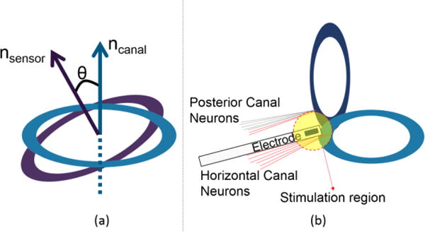
A vestibular prosthesis (VP) can potentially increase the quality-of-life for individuals suffering from bilateral vestibular dysfunction. By replacing the peripheral vestibular organs’ functions, a VP senses 3D angular and linear head motions, using inertial sensors, and selectively stimulates the corresponding vestibular neurons. To improve the efficacy of stimulation, a Vector-Matrix-Multiplier (VMM) block is an essential component of the VP system. A VMM serves to align the primary axes of implanted angular rate sensors with the natural alignment of natural vestibular sense organs (Fig. 1(a)); hence, the VMM performs a coordinate system transformation. Additionally, a VMM mitigates false representations of motion caused by undesired current spread. Resulting from the close proximity of vestibular neurons from adjacent canals (approx. 6 μm), stimulation current targeted for a given canal may excite neural tissue for an adjacent canal (Fig. 1(b)). A VMM can mitigate this effect with a precompensate strategy [1]. Functionally, the VMM operates on the triplet from the rate sensors into appropriate modulation signals by use of a 3-by-3 transformation matrix. This matrix can be characterized by analyzing the eye movements in response to stimuli and selecting transformation weights that maximize the response [1]. In turn, VMM outputs are encoded into frequency modulated control signals, which are directed to a neural stimulator that delivers bi-phasic, charge-balanced current pulses to vestibular neurons [2],[3].
Figure 1.

Vector Matrix Multiplication. (a) To align the primary axes of implanted sensors and peripheral vestibular sense organs, a VMM can perform a coordinate system transformation between the implanted sensors and natural organs. (b) When an electrode is placed to stimulate only horizontal canal neurons, a portion of posterior canal neurons can be stimulated erroneously. To eliminate false representations of motion due to current spread a VMM can precompensate, or adjust, for the effect.
For a VP to provide a sustained therapeutic benefit, continuous stimuli to vestibular neurons is essential [4]. Low power operation is a crucial design parameter. Therefore we have implemented the VMM in the analog domain [5],[6]. While a digital domain solution typically offers ease of implementing complex algorithms and the ability to vary parameters, it comes at the expense of additional analog-to-digital and digital-to-analog conversion circuitry. In our implementation the core operation of the VMM, namely multiplication, is performed using a subthreshold transconductance multiplier. Subthreshold operation combined with processing signals in the analog domain improves the energy-efficiency of the system.
This paper describes the operation and testing results for the low-power VMM. More specifically, in Section II we present the VMM design and follow with VMM performance measures in Section III. The paper concludes with a discussion of the results and addresses future directions for a VMM-VP system in Section IV.
II. VMM Design
In the natural human system, neurons of semicircular canals (SCCs) carry a three-component representation of 3D angular head movements and each SCC is associated with one-component [7]. 3D linear movements are resolved into two separate vector components by the otolith organs. However, we focus on 3D angular head rotations since precompensation is better understood for angular head motion [8]. As an initial precompensation strategy our VMM performs a 3-by-3 vector matrix multiplication of angular rate sensor outputs (gyroscopes).
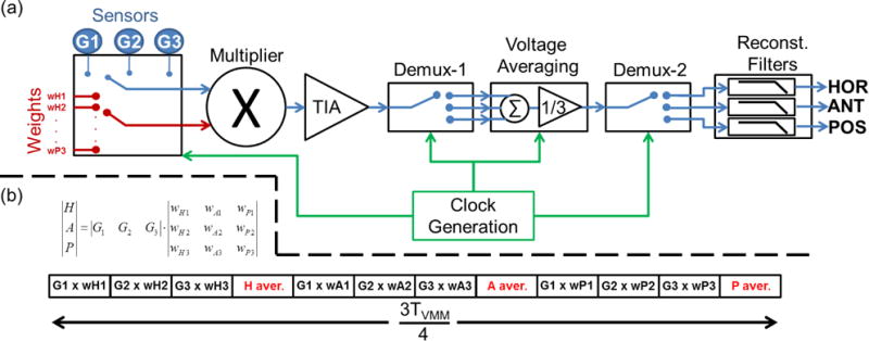
The general block diagram of the VMM is shown in Fig. 2(a). For the nine multiplications needed for a 3-by-3 matrix multiplication, a single multiplier is utilized, but the signals are time-division multiplexed (TDM). This is advantageous since power consumption is reduced and calculation errors due to device mismatches are minimized with a single multipler.
Figure 2.

VMM operation. (a) Block Diagram. (b) The time sequence of each arithmetic operation, where TVMM is the VMM cycle time. HOR, ANT, and POS are the corrected signals for the horizontal, anterior, and posterior canals, respectively. G1, G2, and G3 denote the output signals from the gyroscopes and wj,i denotes the weight voltage corresponding to the canal j, and the gyroscope number i.
Timing of the VMM is presented in Fig. 2(b). The sensor output and the weight voltages (wj,i) are fed to the multiplier periodically. A transimpedance amplifier (TIA) converts current output of the multiplier into voltage. This voltage is demultiplexed periodically in groups of three. In each group, three voltages are added together to generate discrete-time corrected signals for each SCC. A voltage averaging circuitry performs the addition. A second demultiplexer periodically feeds the voltage averaging output to three low-pass reconstruction filters to generate continuous-time corrected signals. A Clock Generation Block (CGB) generates the necessary clocks. In the following sub-sections, operation of each block is explained in detail.
A. Sensor and Weight Voltages Multiplexing
One period of the VMM cycle, TVMM, is divided into 16 equal time intervals. The first 12 intervals are used for multiplication and voltage averaging (Fig. 2(b)). During each of these intervals sensor voltages and weight voltages are fed to the inputs of the multiplier sequentially. To reduce charge injection and clock feedthrough, multiplexing is done over a series of small-sized complementary switches controlled by the CGB. The VMM is idle for the last 4 intervals. The additional circuitry to reset the counter after 12 intervals would consume power and was therefore omitted retaining a 16-interval cycle.
B. Multiplier
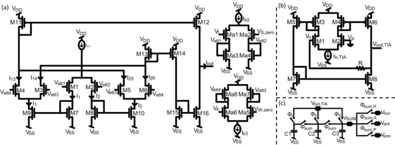
A transconductance multiplier generates current outputs proportional to the product of its voltage inputs; namely, a gyroscope output and a stored weight voltage. The multiplier is a four-quadrant, wide-output-range Gilbert multiplier (Fig. 3(a)) [9]. The multiplier is operated in the subthreshold region with a current characteristic of a MOS in saturation:
| (1) |
where I0 is the zero-bias current, κ the constant relating the surface potential of the MOS to its gate voltage, VGB the gate-to-bulk potential, VSB the source-to-bulk potential, and UT the thermal voltage [10]. After a series of calculations the multiplier output current, Iout is:
| (2) |
To increase the small linear range due to subthreshold operation, input voltages are attenuated at two attenuation stages (Fig. 3(a)) [11]. Each attenuation stage consists of a differential pair in above-threshold region with a diode-connected load in subthreshold region, thereby creating an attenuation factor:
| (3) |
where K is the transconductance parameter, which is a function of mobility and unit gate-oxide capacitance; and Ib is the bias current of the attenuation stage [11]. The bias currents Ib1, Ib2, and Ib3 are generated by an off-chip reference circuitry.
Figure 3.

Multiplier, TIA, and voltage averaging schematics. (a) Multiplier with attenuation stages. (b) TIA. (c) Voltage averaging circuitry.
C. Transimpedance Amplifier
The current output of the multiplier is converted into voltage by a transimpedance amplifier (TIA). The TIA is designed as an operational transconductance amplifier (OTA) with a 1 MΩ resistive negative feedback (Fig. 3(b)).
D. Voltage Averaging and Demultiplexing
The TIA output is demultiplexed to generate three voltages that are arithmetically averaged at voltage averaging circuitry (Fig. 3(c)). At Φ1, Φ2, and Φ3; TIA output is sampled into equal sized sampling capacitors; C1, C2, and C3, respectively. At Φsum, the sampling capacitors are connected in parallel to generate a voltage, VSUM, which is ideally equal to one third of the sum of the voltages stored at the capacitors. However, because of charge leakage during hold periods, the voltage levels at sampling capacitors reduce. The sampling capacitance is set at 5 pF, which is large enough to create negligible error because of charge leakage. Capacitor mismatches also create error. Both leakage and mismatch errors can be compensated by the weight voltages. VSUM is demultiplexed to generate the discrete-time corrected signals corresponding to the three canals, namely Vhor, Vant, and Vpos.
E. Reconstruction Filters
Designed as off-the-chip single-stage RC low-pass filters, the reconstruction filters convert the discrete-time demultiplexer-2 output signals into continuous-time. Op-amp buffer stages prevent the RC network from loading the on-chip circuitry.
F. Clock Generation
The clocks necessary for a 3-by-3 VMM circuitry are generated by a Clock Generation Block (CGB), which consists of D-Flip Flops and various logic gates. The input to the CGB is an external clock. Its period, Tin, must guarantee complete charging/discharging of the voltage averaging capacitors. This is accomplished by the multiplier output current. For typical values (Ib1=50 nA, sampling capacitor of 5 pF, maximum potential change of 100 mV) the gyroscope output and weight voltage sampling interval must exceed 10 μs (100 kHz max. input clock frequency). The upper bound for Tin is determined by the bandwidth requirement of the system. Signals sampled non-ideally at a period of Ts, are distorted in the frequency domain by the sinc(π*f*Ts) function [12]. Similarly, sample-and-hold operation of our system distorts the sensor signals, thereby limiting the bandwidth of the system. Setting Tin=45.4 μs, proper sampling is ensured with a −3 dB bandwidth of f-3dB=1.83 kHz. At that sampling rate, for signals within the frequency range of normal head motions (f < 20 Hz), the distortion is calculated to be less than 40 ppm. One period of VMM operation, namely TVMM is TVMM=16*Tin.
III. VMM Verification
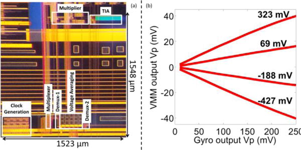
The VMM was fabricated with the TSMC 0.35 μm 4M2P CMOS process (Fig. 4(a)). The system operates with dual power supplies, ±1.6 V, and an external clock of 22 kHz generated using a TI MSP430 series microcontroller (Texas Instruments, Dallas, TX). All bias currents are also generated off-chip with discrete operational amplifier components.
Figure 4.

(a) Optical image of VMM. The footprint is 1523 μm × 1548 μm. However, the effective area covered is less than a quarter of the total footprint. (b) Linear dependence of the VMM output (y-axis) with respect to the input signal magnitudes (x-axis) parameterized by weight voltage (−427 mV to 323 mV, equal weighting applied to all gyro outputs).
A. Linearity
To validate linearity, a sinusoidal signal representing gyroscope output is input to the VMM. This sensor input is multiplied with a range of weight voltages between −427 mV and 323 mV. For a fixed weight voltage, the output signal magnitude varies linearly with the magnitude of the sinusoidal input (Fig. 4(b)). Figure 5 illustrates the output a 10 Hz sinusoidal signal is fed to all three sensor inputs; G1, G2, and G3; and multiplied by the weight elements [1 1 1] and [−1 −1 −1].
Figure 5.

The output waveforms out1 and out2 are obtained when the input is multiplied with the weights [1 1 1] and [−1 −1 −1], respectively.
B. Bandwidth
The bandwidth of the VMM system limits the maximum frequency of linear/angular motion that can be processed. The measured −3 dB frequency of the VMM system is f-3dB,meas=1.25 kHz. The discrepancy between the measured and the calculated (f-3dB=1.83 kHz) values can be attributed to omission of the VMM idle period when calculating the Ts.
C. Power
Based on simulations the VMM power consumption is 5.37 μW, indicating 3.9 nJ of energy consumption per 3-by-3 VMM operation. It should be mentioned that the VMM circuitry was laid out on a die that has other analog circuit blocks as well. Because all analog circuitry on the die were powered by the same supply sources, a direct power measurement of the VMM was not made. For direct power measurement, the same VMM circuit was fabricated with another technology having the same feature size (TI LBC7 0.35 μm 3M2P CMOS process). Supplied by ±1.6 V and operated with an external clock of 10 kHz, the power consumption was measured as 5.1 μW, indicating 8.16 nJ of energy consumption per 3-by-3 VMM operation. The difference between the measured and simulated power values can be attributed to the higher clock frequency (22 kHz) of the TSMC chip. For comparison with an off-the-shelf low-power, signal processor, a TI MSP430 series microcontroller was used to implement an analog-input and analog-output VMM. With an ADC sampling rate of 220 Hz, the microcontroller consumes 6 mW of power. It should be noted that to make a more realistic comparison between our system and the microcontroller, supporting blocks; namely memory, reference, and DAC; need to be designed. However, with careful design of those blocks, current consumption of the custom chip could still be kept in the sub-mW range.
IV. Conclusion
A 3-by-3 VMM system using low-power analog signal processing techniques has been demonstrated. To utilize the VMM in an actual implant; bias circuitry, reconstruction filters, and an oscillator for the CGB need to be on-chip. For a fully implanted system, patient-dependent transformation matrix elements can be fed to the VMM using capacitors refreshed periodically by charge-sharing DACs that generate analog voltages from weight values digitally stored at a memory element. In an actual VP, the weight elements need to be stored only once, after the implantation. Therefore, as long as the weight voltage-output relationship of the VMM is well characterized, the asymmetry observed at the multiplication output for negative and positive weight voltages due to device mismatches will not affect the operation of the VMM.
Reducing the number of multiplier-TIA pairs improves the energy-efficiency significantly but also reduces bandwidth. However, when considering the low-frequency nature of normal head motions (<20 Hz), this reduction in bandwidth will not affect the target vestibular application.
Clinical vestibular studies suggest that normal angular and linear head motions are within ±500 °/sec and ±5 g range [13],[14]. We designed our system to interface with commercial analog-output accelerometers and gyroscopes with sensitivities less than 0.5 mV/°/sec and 50 mV/g, respectively. It should be noted that the multiplier attenuation circuitry in the VMM increases the input dynamic range by 300% in order to process such signals, but at the cost of increasing the power consumption by 2.24 μW. The system power could be reduced dramatically if rate sensors with sensitivities less than 0.1 mV/°/sec and 10 mV/g were employed. As a result the need for attenuation circuitry would be eliminated thereby reducing the total power by more than 40%.
Acknowledgments
The authors thank Professors Oliver Brand and Saibal Mukhopadhyay, and students Hommood Alrowais, Sergio Carlo, Kevin Pham, Jin-Jyh Su, and Wen Yueh at the Georgia Institute of Technology for help with testing as well as alumni Drs. Kemal Demirci and Gokce Gurun.
This work was supported in part by the National Science Foundation under Grant ECCS-0927103, CAREER ECCS-1055801, and by the National Center for Advancing Translational Sciences of the National Institutes of Health under Award Number UL1TR000454, KL2TR000455.
References
- 1.Fridman GY, Davidovics NS, Dai C, Migliaccio AA, Della Santina CC. Vestibulo-ocular reflex responses to a multichannel vestibular prosthesis incorporating a 3-D coordinate transformation for correction of misalignment. JARO. 2010 Sep;11(3):367–381. doi: 10.1007/s10162-010-0208-5. [DOI] [PMC free article] [PubMed] [Google Scholar]
- 2.Töreyin H, Bhatti PT. A field-programmable analog array development platform for vestibular prosthesis signal processing. IEEE Transactions on Biomedical Circuits & Systems. 2013;7(3):319–325. doi: 10.1109/TBCAS.2012.2216525. [DOI] [PMC free article] [PubMed] [Google Scholar]
- 3.Bhatti P, Toreyin H, Hasler P. Proc of the 8th IASTED International Conference on Biomedical Engineering. ACTA Press; 2011. A neural stimulator for a vestibular prosthesis utilizing a low-power field-programmable analog array; pp. 723–097. [Google Scholar]
- 4.Fridman G, Della Santina C. Progress toward development of a multichannel vestibular prosthesis for treatment of bilateral vestibular deficiency. The Anatomical Record. 2012;295:2010–2029. doi: 10.1002/ar.22581. [DOI] [PMC free article] [PubMed] [Google Scholar]
- 5.Mead C. Neuromorphic Electronic Systems. Proc IEEE. 1990 Oct;78(10):1629–1636. [Google Scholar]
- 6.Schlottmann C, Hasler P. A highly dense, low power, programmable analog vector-matrix multiplier: The FPAA implementation. IEEE J Emerging Sel Topics Circuits Syst. 2011 Sep;1(3):403–411. [Google Scholar]
- 7.Rabbitt RD. Directional coding of three-dimensional movements by the vestibular semicircular canals. Biological Cybernetics. 1999 Jun;80:417–431. doi: 10.1007/s004220050536. [DOI] [PubMed] [Google Scholar]
- 8.Lewis RF, Haburcakova C, Gong W, Lee D, Merfeld D. Electrical stimulation of semicircular canal afferents affects the perception of head orientation. Journal of Neuroscience. 2013;33(22):9530–9535. doi: 10.1523/JNEUROSCI.0112-13.2013. [DOI] [PMC free article] [PubMed] [Google Scholar]
- 9.Mead C. Analog VLSI and Neural Systems. Reading, MA: Addison-Wesley; 1989. pp. 94–96. [Google Scholar]
- 10.Harrison RR. class notes for ECE 5720. Department of Electrical and Computer Engineering, The University of Utah; Spring. 2010. The MOS Transistor in Weak Inversion. [Google Scholar]
- 11.DeWeerth S, Patel G. Variable linear-range subthreshold OTA. Electron Lett. 1997;33(15):1309–1311. [Google Scholar]
- 12.Plett C. class notes for ECE 97.477. Department of Electrical and Computer Engineering, Carleton University; Winter. 2000. Sampled Data Basics. [Google Scholar]
- 13.Baird RA, et al. The vestibular nerve of the chinchilla. II. Relation between afferent response properties and peripheral innervation patterns in the semicircular canals. J Neurophysiol. 1988 Jul;60(1):182–203. doi: 10.1152/jn.1988.60.1.182. [DOI] [PubMed] [Google Scholar]
- 14.Fernandez C, Goldberg JM. Physiology of peripheral neurons innervating otolith organs of the squirrel monkey. II. Directional selectivity and force response relations. J Neurophysiol. 1976;39:985–995. doi: 10.1152/jn.1976.39.5.985. [DOI] [PubMed] [Google Scholar]


