

Abstract
We report how the presence of electron-beam-induced sulfur vacancies affects first-order Raman modes and correlate the effects with the evolution of the in situ transmission-electron microscopy two-terminal conductivity of monolayer MoS2 under electron irradiation. We observe a red-shift in the E′ Raman peak and a less pronounced blue-shift in the A′1 peak with increasing electron dose. Using energy-dispersive X-ray spectroscopy and selected-area electron diffraction, we show that irradiation causes partial removal of sulfur and correlate the dependence of the Raman peak shifts with S vacancy density (a few %). This allows us to quantitatively correlate the frequency shifts with vacancy concentration, as rationalized by first-principles density functional theory calculations. In situ device current measurements show an exponential decrease in channel current upon irradiation. Our analysis demonstrates that the observed frequency shifts are intrinsic properties of the defective systems and that Raman spectroscopy can be used as a quantitative diagnostic tool to characterize MoS2-based transport channels.
Keywords: MoS2, two-dimensional material, Raman, in situ transmission electron microscopy, transition-metal dichalcogenide
Graphical abstract
The study of two-dimensional transition-metal dichalcogenide films has attracted much attention recently due to their interesting electrical and optical properties,1,2 including semiconducting behavior with a band gap that evolves from indirect in the bulk and few layers to direct in a single layer.3,4 In particular, MoS2 has been identified as a promising material due to large current on/off ratios in field-effect transistors (FETs),5 strong photoluminescence,6 electroluminescence,7 and methods of large-area synthesis of monolayers.8 MoS2 FETs have been reported with carrier mobilities comparable to those in graphene nanoribbons and with current on/off ratios as high as 108 at room temperature.5 In addition, MoS2 FETs have been used in integrated circuits9,10 and have also been suggested as sensors for DNA sequencing.11
Defects in MoS2 can be introduced during exfoliation, chemical-vapor deposition (CVD) growth,12 transfer, and electron irradiation. These defects are expected to deteriorate the device quality of MoS2. For example, monosulfur vacancies are known to act as compensation centers in n-type MoS2.12 On the other hand, defects in MoS2 can also have a beneficial impact on material properties. For instance, defects have been shown to be the dominant dopant in MoS2, with natural defect variation allowing n-type and p-type regions to coexist across distinct regions of the same sample.13 In addition, the metallic character of sulfur vacancies can lower Schottky barrier heights when MoS2 is placed in contact with certain metals, where at a defect coverage of just 0.3% the junction current is dominated by the lower Shottky barrier of the defects.13,14 Given their importance on device properties, it is crucial to fully characterize defects in MoS2 in order to develop a reliable diagnostic tool for future large-scale deployment of MoS2-based electronics.
In this article, we present measurements and simulations of the first-order Raman modes of monolayer MoS2 with varying amounts of electron-beam-induced sulfur vacancies, as well as corresponding in situ transmission-electron-microscopy (TEM) current–voltage measurements. We find that the frequency separation between the first-order Raman modes, E′ and A′1, increases as sulfur vacancies are introduced. This trend is captured by ab initio density functional theory (DFT) calculations and determined to be largely related to changes in the system’s restoring force constant due to S vacancies. We observe preferential sulfur sputtering as a function of electron dose using energy-dispersive X-ray spectroscopy (EDS) in the TEM and quantify these results with selected-area electron diffraction (SAED). We establish by in situ electrical current measurements a concomitant exponential decrease in channel current upon MoS2 degradation by the electron beam. Our results demonstrate how Raman spectroscopy can be used as a quantitative and nondestructive characterization tool of S vacancies in MoS2.
RESULTS AND DISCUSSION
Figure 1 shows typical MoS2 devices and the corresponding experimental setup. Single-crystal, monolayer MoS2 flakes were grown8,15 by CVD and transferred to Si3N4/Si chips16 for in situ TEM measurements. A schematic diagram of the MoS2 device exposed to the electron beam in the TEM is illustrated in Figure 1a. The sample orientation in the TEM is such that the electron beam hits the Si3N4 membrane first and exits through the MoS2. The in situ TEM holder consists of six electrical feedthroughs allowing three pairs of Au electrodes to be wired up to the sample holder (inset of Figure 1a). Figures 1b,c present scanning electron micrographs and an optical image of the chip surface. They show the Si3N4 membrane at the center, suspended on the Si chip and covered by MoS2 triangular monolayers, which are contacted by the Au electrodes. The crystalline lattice of the MoS2 used in this work is revealed by performing aberration-corrected scanning TEM (AC-STEM) imaging on MoS2 flakes deposited on holey-carbon grids (Figure 1d).
Figure 1.

Device schematic and experimental setup. (a) Illustrative diagram of the MoS2 device exposed to the electron beam in the TEM. The arrow indicates that the electron beam enters through the SiNx and exits through the MoS2. Inset: Optical micrograph of the TEM holder with six electrical leads used for in situ current measurements (scale bar 3 mm). (b) Scanning electron micrographs (SEM) of the chip surface showing the suspended Si3N4 membrane in the center (black square) and many MoS2 flakes (dark gray) on the surface; Au wires appear white. Inset: SEM with larger MoS2 flakes (JEOL JSM-6400) (scale bars 100 µm). (c) Optical image of the Si3N4/Si chip containing three pairs of Au electrodes contacting the MoS2 flakes on the Si3N4 membrane (scale bar 10 µm). (d) Aberration-corrected TEM image of freestanding MoS2 used in this work (JEOL ARM 200CF) (scale bar 2 nm).
Bulk MoS2 is characterized by two prominent Raman-active modes, E2g1 and A1g. The notation for these modes becomes E′ and A′1 in monolayer MoS2 due to a change in crystal symmetry.17–19 To study the effects of electron-beam irradiation on the E′ and A′1 Raman modes of monolayer MoS2, we transferred CVD-grown MoS2 flakes onto 100 nm thick Si3N4 windows (Figure 2a), allowing for in situ irradiation at doses ranging from 1 × 10⁴ to 1 × 10⁸ electrons nm−2. After insertion into the TEM, the entire area of each sample was subjected to a small electron dose, estimated at less than 1 × 10³ electrons nm−2. Samples were irradiated by spreading the circular beam to diameters of 2–12 µm. Raman maps were taken in ambient conditions immediately following TEM exposure. A 532 nm excitation wavelength was used. The laser power was set to 2 mW for recording large-area maps on some samples and was kept below 0.3 mW for long exposures on other samples. These laser powers were not found to affect the Raman peaks, as detailed in SI Section 1.
Figure 2.

Raman mapping of the MoS2 device showing the effects of irradiation on the E′ and A′1 Raman modes. (a) Optical image of a MoS2 flake on top of a Si3N4 window. Six circles outline the electron-irradiated regions with doses (clockwise from top right, in electrons nm−2) of 1 × 10⁴, 5 × 10⁴, 1 × 10⁵, 5 × 10⁵, 1 × 10⁶, and 5 × 10⁶. The gold contacts were used as visual aids in the TEM. The MoS2 flake is outlined and the brightness slightly increased for visual clarity. (b) Series of corresponding Raman spectra (dotted lines) and Lorentzian fits (solid lines) for the low-dose region (green), for 5 × 10⁵ electrons nm−2 (orange), and for 5 × 10⁶ electrons nm−2 (purple). (c) (i–vi) Spatial maps of the peak shift, amplitude, and fwhm of the E′ and A′1 modes, respectively, across the device surface. (vii–ix) Spatial maps of the E′ and A′1 peak separation, ratio of peak amplitudes, and ratio of peak fwhm’s. All scale bars are 10 µm. Pixels outside the MoS2 flake were not plotted. The white circle in the middle of the flake is where material was mistakenly removed by the Raman laser and should be ignored. Outlines of the irradiated areas are shown in (v). Each diverging color map was shifted so the brightest portion would match the corresponding value of the pristine MoS2 region, so that the pristine region is the same color in each figure.
Representative Raman spectra of MoS2 in the low-, medium-, and high-dose regimes are reproduced in Figure 2b. The spectra clearly highlight the Raman mode shifts upon irradiation. Further, Figures 2c(i–vi) show the evolution of the peak shift, amplitude and full-width at half-maximum (fwhm) for the E′ and A′1 modes. The separation between the E′ and A′1 modes is provided along with the amplitude and fwhm ratios in Figures 2c(vii–ix). A number of clear effects of electron irradiation can be seen in Figure 2c. The A′1 peak is initially slightly blue-shifted and then red-shifted back to almost its original position (Figure 2c(iv)). The E′ peak is notably redshifted with increasing dose (Figure 2c(i)). This observation establishes that electron irradiation causes a notable increase in the separation between the E′ and A′1 modes for high-dose regions (Figure 2c(vii)). Raman maps of additional flakes are presented in SI Section 2.
In a previous report, suspended, monolayer MoS2 was irradiated in an aberration-corrected TEM, allowing single S vacancy defects to be counted visually. In that study, the TEM irradiation of MoS2 was shown to produce mainly monosulfur vacancies.20 Here, we use this result and assume that the majority of defects produced in our experiments are monosulfur vacancies (rather than Mo vacancies or large holes). This assumption is supported by EDS and SAED measurements, as discussed below. One major difficulty related to the use of electron irradiation to induce defects is to quantitatively relate the electron dose with the actual defect concentration (Vs) present on the sample. To address this issue, we performed EDS to monitor the elemental composition within the illuminated region as a function of electron dose. Results obtained with 200 keV electrons are shown in Figure 3. The EDS measurements were performed on a monolayer region with the beam spread over a 1.6 µm diameter. The EDS measurements (Figures 3b,c) indicate that the S:Mo atomic ratio starts at a value close to the stoichiometric 2:1 as expected for a low-defect sample and then drops, thereby showing that the material starts with a low defect density and that S atoms are preferentially sputtered. We further discuss the initial nonzero S defect density below. The net intensity of the Mo signal remains constant during the 60 minute irradiation, supporting the fact that the main effect of irradiation is to create S vacancies and that Mo atoms are much more difficult to sputter.
Figure 3.

Estimate of the sulfur sputtering cross-section. (a) EDS spectrum of monolayer MoS2 on a holey carbon grid. (b) Measured EDS intensity of sulfur and molybdenum as a function of electron dose. The S intensity drops while the Mo intensity remains constant. (c) EDS-measured stoichiometry, showing an initial value of S/Mo = 2.01 ± 0.07, as expected for CVD-grown MoS2 where a small amount of S vacancy (~0.5%) can be present after growth. (d) Inverted SAED pattern of pristine, monolayer MoS2 on a 100 nm thick Si3N4 substrate. (e) Sum of the intensity of the visible [1̅100] peaks. A fit to eq SI 4.1 gives an S sputtering cross-section of 75 ± 10 barn. (e) Sum of the intensity of the visible [2̅110] peaks. A fit to eq SI 4.1 gives an S sputtering cross-section of 120 ± 20 barn. Note that we fit the SAED data only at low doses (less than 2 × 10⁷ electrons nm−2).
In addition, we performed SAED measurements to further support our EDS results. The SAED measurements were performed on a monolayer region with the beam spread over a 3.2 µm diameter area and a selected-area aperture of 1 µm centered on the middle of the beam. Figures 3e,f show the drop in SAED intensities of the [1̅100] and [2̅110] spots as a function of electron dose. Because the crystal is monolayer, we can fit the measured intensity drops to kinematic diffraction intensities of MoS2 with monosulfur vacancies, as outlined in SI Section 4. The maximum dose used for Raman measurements was 1 × 10⁷ electrons nm−2, so to capture the sputtering behavior in this low-damage regime, we fit only the SAED data at low doses (less than 2 × 10⁷ electrons nm−2). This fit provides an estimate of S sputtering cross-section at 75 ± 10 barn for the [1̅100] family and 120 ± 10 barn for the [2̅110] family. These measured sputtering cross-sections are consistent with a previous study that measured the S sputtering cross-section as 1.8 barn with an 80 keV accelerating voltage and calculated it to be ~140 barn at 200 keV for free-standing monolayer MoS2.20 As the previous cross-section measurement was taken on a small (<100 nm2), pristine, and suspended area of MoS2, we expect our lower values for the S sputtering cross-section are due to contamination left on the surface from the PMMA transfer. For the remainder of this paper, we will use the SAED measured cross-section of 75 ± 10 barn for all quantitative analyses. Note that using our measured sputtering cross-section gives the lower bound on total defect formation, as other types of defects, e.g., line defects21 and defects created by beam-induced chemical etching,22 are likely to become non-negligible at high doses. It follows that estimates of defect density using S vacancy as the only source of defects can be considered as a lower bound for the defect density. In addition, we verified that after irradiating at doses of 2 × 10⁷ electrons nm−2 followed by removing the sample from the TEM and exposing it to the atmosphere for 10 min, the lattice was left intact and no small or large holes were observed. Therefore, at irradiation doses probed by Raman in this work, the defects were dominated by monosulfur vacancies and possibly line defects.
In a previous work, the initial sulfur vacancy concentration in CVD-grown MoS2 was measured with AC-STEM.23 In CVD samples from multiple laboratories, postgrowth defects were mainly monosulfur vacancies at a concentration of (mean, standard deviation) = (0.134 nm−2,0.05 nm−2). This corresponds to an initial Vs = 0.5%. Our flakes grown by CVD are consistent with this. The EDS measurements (Figure 3c) show an initial stoichiometry of S/Mo = 2.01 ± 0.07. Therefore, it seems reasonable to use an initial defect density VS = 0.5% in our quantitative analysis shown below.
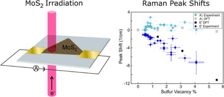
Figures 4a,b show the shift of the E′ and A′1 modes and the increase in separation between the two modes as a function of sulfur vacancy concentration, respectively. The S vacancy concentration was calculated using the measured 75 barn sputtering cross-section, the electron dose, and the methods outlined in SI Section 3. For doses greater than 1.0 × 10⁷ electrons nm−2, corresponding to a sulfur vacancy concentration of 4%, the E′ and A′1 peaks are no longer visible on top of the SiNx background with the laser conditions used for Raman mapping. This result of increasing peak separation vs defect concentration compares well with studies of Raman modes of ion-irradiated24 and reactive-ion-etched25 MoS2, where similar shifts in each mode were observed as a function of damage. In these previous reports, the defects created by the ion beam or plasma etching were likely much larger than single-point defects. In contrast, our work shows shifts in the Raman modes due to monosulfur point defects and line defects.
Figure 4.

Raman peak shift vs S vacancy: experiment and theory. (a) Experimental and theoretical individual peak shifts of the E′ and A′1 modes as a function of sulfur vacancy percentage. The experimental (blue and sky blue) defect concentration is calculated using the irradiation dose, the measured 75 ± 10 barn sputtering cross-section, and the methods outlined in SI Section 3. DFT calculations are shown in gray and black. (b) Change in separation between the E′ and A′1 Raman modes as a function of defect concentration.
In addition to sputtering, it is well known that TEM irradiation causes amorphous carbon deposition26,27 and sample charging.28 In MoS2, the separation between the E′ and A′1 modes increases from monolayer to bulk.18,19 In fact, an increase in peak separation can be seen in multilayer regions in the upper-right-hand portion of Figure 2c(vii) and in the middle of Figure SI 2.1c(vii). To rule out thickness-dependent effects in monolayer regions, including effects related to beam deposition of amorphous carbon that might act in a way similar to the increase in separation from monolayer to bulk, we recorded Raman spectra before and after depositing 5 nm of amorphous carbon outside of the TEM using normal sputtering techniques. Figure SI 5.1 shows that the positions of the Raman modes are unaffected by this amorphous carbon deposition. Finally, because it is established that doping softens the A′1 mode,29 our measurements that irradiation mostly affects the E′ mode allow us to dismiss charging effects.
We have carried out first-principles DFT calculations to establish the microscopic origin of the experimentally observed Raman peak shifts as a function of the electron irradiation dose. Monolayer, pristine MoS2 belongs to space group P6m2 (No. 187), and its two characteristic Raman active modes are E′ (~384 cm−1) and A′1 (~403 cm−1), as discussed previously.17–19 Creating monosulfur vacancies reduces the symmetry of the system, and the symmetry assignments of Raman modes change as well. For simplicity and consistency, the notations E′ and A′1 are used for all defective systems. Simply speaking, removing an atom from a system weakens the restoring force constant of a phonon mode, but the total mass of the system is reduced as well. As the frequency (ω) is positively correlated to the restoring force constant (K) yet inversely correlated to the total mass (m) (i.e., for a simple harmonic oscillator we would have ), the phonon mode frequency can be either increased or decreased depending on which factor is reduced more. To understand how VS affects the E′ and A′1 modes in monolayer MoS2 in an extreme case, we first chose the MoS2 primitive unit cell and calculated phonon frequencies for the pristine system (VS = 0%) and the one with single S atom removed (i.e., top layer or VS = 50%), as shown in Figure SI 6.1. For the pristine system, the E′ mode corresponds to opposite in-plane vibrations of Mo and S atoms (i.e., in-plane vibrations of two Mo–S bonds). In the case of Vs = 50%, the removal of the top S atom leads to vibration of only one Mo–S bond and thus a significantly weaker restoring force constant and lower E′ phonon frequency (Figure SI 6.1). Our calculations show that the frequency of the E′ mode is decreased by 100.6 cm−1 from Vs = 0% to Vs = 50%. In contrast, the A′1 mode corresponds to out-of-plane vibrations of the Mo–S bonds with static center Mo atoms for the pristine system. Thus, the removal of the top S atom leads to a missing Mo–S bond (weakening the restoring force constant compared to the pristine system), while allowing the originally static Mo atom to vibrate out of plane (which strengthens the restoring force constant from the Mo–S bond vibration), as shown in Figure SI 6.1. This simple picture shows that the overall restoring force constant could be increased or decreased. In fact, our calculations show that the frequency of the A′1 mode is increased by 42.3 cm−1 from VS = 0% to VS = 50%. Such a frequency increase could also be due to the reduced mass. To find out if the mass is the deciding factor in this case, we derived the force constant based on the simple model K = mω2. For 0% VS, m = mMo + 2mS; for 50% VS, m = mMo + mS, where mMo = 3mS. From VS = 0% to VS = 50%, the total mass is reduced by 20%. From the total mass and computed frequencies, it is found that from VS = 0% to VS = 50%, the restoring force constant of the E′ mode is reduced by ~55.8%, while the restoring force constant of the A′1 mode is reduced only by ~2.7%. Clearly, the restoring force constant of the E′ mode is indeed dramatically weakened (much larger than the mass reduction, hence the significant frequency decrease). Conversely, the restoring force of the A′1 mode is only mildly reduced due to its unique vibration pattern, and it follows that its frequency decrease is mainly due to the mass reduction (more details are provided in Figure SI 6.1). Note that VS = 50% means the removal of the whole top S layer, an unlikely case in reality, but such an extreme case illustrates the mechanisms of how E′ and A′1 Raman modes evolve with the VS concentration in general.
To model different experimentally accessible VS concentrations in monolayer MoS2, supercells of different sizes were selected with a single S atom removed in each supercell. We have considered single defects in a 6 × 6 supercell (VS = 1.4%), a 4 × 4 supercell (VS = 3.1%), and a 3 × 3 supercell (VS = 5.6%), as shown in Figure SI 6.1. Note that the vacancy concentration is computed as the number of S vacancy sites divided by the total number of S atoms in the supercell of the pristine system. For example, in the 6 × 6 supercell, the top S layer has 35 sulfur atoms and one vacancy, resulting in VS = 1/72 = 1.4%. As discussed above, the restoring force constant of the E′ mode is expected to be weakened due to missing Mo–S bonds. Indeed, the calculated frequency of the E′ mode is reduced slightly by 1.55 cm−1 (black square in Figure 4a). With increasing VS concentration, there are fewer Mo–S bonds involved in the in-plane vibrations, and thus the restoring force constant of the E′ mode is continuously weakened (more than the mass reduction). Hence, the calculated frequency of the E′ mode is continuously red-shifted with increasing VS, consistent with the experimentally observed trend (blue circles in Figure 4a). The mechanism is different for the A′1 mode, since it has a significantly different vibration pattern compared to E′, so that its restoring force constant is only slightly reduced. On the other hand, the total mass of the system is also mildly reduced with increasing VS. These two competing factors both affect the position of the A′1 mode, giving the A′1 frequency a more complex dependence on VS concentration. Our calculations show that with increasing vacancy concentration, the frequency of the A′1 mode first upshifts slightly and then downshifts (gray squares in Figure 4a), suggesting the competition of multiple factors. We note that the formation of line defects could also play a role, as discussed below. The predicted trend is in agreement with the experimental observation (sky blue circles in Figure 4a). This could also explain why the magnitude of the frequency shift of the A′1 mode is not as large as that of the E′ mode. Hence, the E′ mode potentially provides a better handle on the determination of defect density. However, the separation between the E′ and A′1 peaks is also a good indicator of the presence of defects. This is confirmed by the plot shown in Figure 4b, which indicates that the peak separation increases with the VS concentration in both experiment and theory. Our experimental and theoretical Raman results clearly show that the electron beam removes sulfur from the lattice, leading to noticeable Raman peak shifts. Consequently, Raman can be used as an inexpensive and quick probe of local defect concentrations.
Thus, far, we have discussed the simple case of S vacancy. However, a number of mechanisms can occur during experimental measurements that could potentially modify the Raman spectra. For instance, oxygen atoms could fill the S vacancy sites during Raman measurements.30 For this reason, we have also modeled how O substitutional impurities would affect the Raman peaks, using a 4 × 4 supercell with the S vacancy site substituted with an O atom (more details are provided in SI Section 9). Our calculations indicate the O substitution partially restores the bonding, so the E′ peak is not downshifted as much (by ~30%), but it is still notably downshifted. Thus, the O substitution cannot fully restore the Raman peak positions of the pristine system and would still be detected as a vacancy from the Raman peak shifts.
Finally, it has been shown that line of S vacancies can be expected, especially for high irradiation dose.21 We performed additional DFT calculations to examine the effect of aggregated defect patterns on Raman peaks, starting from the 4 × 4 MoS2 supercell with different defect patterns: (1) two separated S vacancies, (2) two neighboring point S vacancies, and (3) four S vacancies forming a line defect, as shown in Table SI 9.1. Comparing the two separated defects and the two neighboring defects patterns, we find only a small difference in the frequency shift of the E′ peak, indicating that the defect configuration has little effect on the E′ peak shift. Moving to four S vacancies forming a line defect, since the vacancy concentration is doubled, the E′ peak downshift is significantly increased (in fact, it is roughly doubled), consistent with the predicted trend of the E′ peak shift versus isolated S vacancy concentration plotted in Figure 4. This again suggests that the effect of line defects on the E′ peak shift is similar to the effect of isolated point defects. Therefore, we expect that the shift in the E′ peak is a good indicator of the defect density, regardless of the detailed defect structure. In contrast, the S vacancy pattern could have a notable effect on the A′1 peak. We find that this peak is no longer upshifted when two S vacancies are formed together; instead it is downshifted. For the line defect studied, it is also downshifted. This lends support to the possibility that the experimentally observed initial larger upshift of the A′1 peak followed by a less pronounced upshift in Figure 4 is partly due to the formation of line defects. As noted above, with increasing irradiation and S vacancy concentration, line defects tend to form, possibly contributing to the decrease of the upshift of the A′1 peak. Nevertheless, the A′1 peak is always upshifted experimentally, suggesting that line defects are not dominant. Due to the smaller and more complicated shifts of the A′1 peak, we expect that the E′ peak shift could be a more reliable indicator of the defect density. In particular, the E′ peak shift is almost insensitive to defect type, providing a universal approach to determine the defect density.
Moving to electronic transport, it was recently demonstrated that the electrical properties of monolayer MoS2 crystals can be tuned via stoichiometry engineering and tailored for specific applications.31 While that work modifies the stoichiometry by changing growth conditions, here we focus on the electrical properties of the irradiated sample. Figure 5 shows the room-temperature, in situ TEM two-terminal measurement (current vs time and dose) of the MoS2 monolayer on top of Si3N4 as a function of electron dose. Thermally evaporated 5 nm/40 nm Cr/Au contacts were used. We observe a quasi-exponential conductance decrease with dose for a constant beam current density (device in Figure 5 biased at 4 V). To confirm that changes in channel current were caused by modifications to the MoS2, and not just by the presence of the beam, we closed the electron beam valve several times to temporarily stop irradiation. While the conductance decrease of the MoS2 after each irradiation period is irreversible, the conductance remains constant while the electron beam valve is closed, as shown by the plateaus in Figure 5b. This is an important observation since it confirms that the conductance change is due to the presence of defects rather than beam-induced charging of the Si3N4 substrate.
Figure 5.

Current decrease during electron irradiation for a constant applied voltage. (a) Room-temperature current measured in a two-terminal configuration of the MoS2 monolayer biased at 4 V on Si3N4 vs electron dose after the electron beam valve is opened and the device is exposed to a constant electron irradiation current (j = 3000 electrons nm−2 s−1). Inset: Optical image of the measured MoS2 device. (b) Data from (a) showing additional time periods where the electron beam valve was closed. The device current remains constant when electron irradiation is stopped, as shown by the measured current plateaus. (c) Simulated normalized conductivity (σ/σo) of a honeycomb resistor network vs the fraction modified sites (p). Sites are modified by multiplying the resistance of the nearest-neighbor bonds by 5, 10, 100, or 1000 or removing the bonds completely.
Sulfur vacancies are expected to have a strong influence on the electronic properties of monolayer MoS2. To better understand this effect, we employed DFT to calculate the electronic band structures of the 6 × 6 supercell with a monosulfur vacancy and the 4 × 4 supercell with a monosulfur vacancy, as shown in Figure SI 7.1. Pristine MoS2 has a direct band gap of 1.85 eV at the K point, and the presence of a sulfur vacancy in the supercells induces several defect bands in the band gap (denoted as VS bands and highlighted in red color in Figure S2). Specifically, there is a S-vacancy-induced band right above the valence band of pristine MoS2, which is the valence band maximum (VBM) of defective MoS2; there are two nearly degenerate bands due to sulfur vacancies below the conduction band of pristine MoS2, which are the conduction band minimum (CBM) and CBM+1 of defective MoS2. Hence in the defective systems, VBM–1 and CBM+2 correspond to the band edges of pristine MoS2. As shown in Figure SI 7.1, compared to the pristine system’s band edges, where the charge densities are delocalized with almost uniform distributions across the layer, the in-gap VS bands (VBM, CBM, and CBM+1 in red) are nearly dispersionless and their charge densities are well localized around VS sites, consistent with a previous report.32 Therefore, an electron or hole occupying these vacancy-induced localized states will be trapped around VS sites with a low carrier mobility, thereby being unable to contribute significantly to electrical transport. Instead, according to a previous theoretical work, these localized states act as scattering centers and can significantly reduce the average conductivity of the system.33 This analysis shows that the introduction of sulfur vacancies can explain the observed decrease in two-terminal conductance during electron irradiation. Using a classical picture, the presence of a S vacancy can be seen as the presence of large local electrical resistors in an initially pristine 2D network. We tested this simple model using a resistance network approach (or percolating network) to test how the random inclusion of defects acting as strong scatterers affects overall transport. The results shown in Figure 5c indicate a good qualitative agreement with the measurements, i.e., a quasi-exponential decrease in conductance as a function of defect generation. Because the experimental results were obtained in the two-terminal configuration, other effects such as changes to the contact resistance during irradiation may contribute to the decrease in device conductivity in highly irradiated samples. We provide this preliminary observation and analysis of resistance changes upon irradiation as a motivation for further research into the electrical response of sulfur vacancies in MoS2.
CONCLUSIONS
In conclusion, we have fabricated two-terminal devices containing micrometer-scale, single-layer MoS2 flakes connected to gold leads on silicon nitride membranes and measured their Raman modes and electrical resistance as a function of electron irradiation. This allowed us to experimentally and theoretically study the effects of electron-beam-induced sulfur vacancies on the electrical and optical properties of MoS2 devices. Our EDS, SAED, and DFT results suggest that electron irradiation produces mainly monosulfur defects. We found that creating monosulfur defect vacancies in MoS2 increases the separation between the E′ and A′1 Raman modes in a quantitative and predictive way. Raman can therefore be used as a nondestructive method for estimating the defect concentration in MoS2. Defects and vacancies have important ramifications for MoS2 device physics, particularly for nanoelectronic applications such as transistors and sensors, frequently requiring electron- or ion-beam exposure of the device. As shown in this work, a small defect density has a characteristic and quantifiable impact on electrical and optical properties.
METHODS
MoS2 Growth
Single-crystal MoS2 flakes were grown directly on a 300 nm SiO2/Si substrate by chemical vapor deposition. A 1% sodium cholate solution is initially spin coated onto the SiO2 substrate to help promote a growth region. A microdroplet of a saturated solution of ammonium heptamolybdate (AHM) is deposited onto the corner of the substrate. The AHM will act as the molybdenum feedstock. The substrate is placed in the center of a 1 in. Lindberg blue furnace, and 25 mg of solid sulfur (part number 213292, SigmaAldrich) is placed upstream at a distance of 18 cm from the growth substrate. Nitrogen (700 sccm) is passed through the chamber, the temperature of the furnace is ramped up to 800 °C, and the sulfur pellet is heated to 150 °C. After a 30 min growth, the furnace is then stopped and rapidly cooled to room temperature.
Device Fabrication
Figure 1 shows the MoS2 devices and the experimental setup discussed above.
MoS2 triangles were first grown on SiO2/Si substrates by chemical-vapor deposition.8 MoS2 was then transferred onto 100 nm thick Si3N4 TEM windows16 using a standard wet KOH method.34 Electrical contacts were fabricated by electron-beam lithography followed by thermal evaporation of 5 nm Cr and 40–100 nm Au.
In Situ TEM Measurements
Observations and electron irradiations were carried out in a JEOL 2100 or a JEOL 2010F operated at 200 kV. The phosphor screen was used to measure the beam current density at each magnification when the beam was expanded to the size of the screen. Any inaccuracy in the beam current measurement will affect the measurements of the S sputtering cross-sections. However, in the expression for vacancy percentage in SI Section 3, the beam current and sputtering cross-section only appear when multiplied together, so inaccuracies in the beam current measurements and S sputtering cross-sections will not affect the estimation of the S vacancy percentage.
EDS measurements were performed in a JEOL 2010F. MoS2 flakes were transferred onto amorphous-carbon grids instead of Si3N4 to reduce the background signal. Spectra were captured and analyzed using EDAX TEAM EDS analysis software.
SAED images were taken in a JEOL 2100 TEM operated at 200 kV. A selected area aperture of effective diameter 1 µm was used. Radial and tangential line profiles were taken across each of the spots. Backgrounds were subtracted using adaptive iteratively reweighted penalized least squares35 (arPLS). The line profiles were fit with Gaussians, and then the spot intensity was determined as the area under the 2D Gaussian defined by the radial and tangential Gaussians. All data was normalized to the diffuse SiNx background intensity.
For in situ TEM electrical measurements samples were mounted in a six-terminal sample holder (Hummingbird Scientific) with electrical feedthroughs, which were connected to a source meter (Keithley Instruments).
AC-TEM of suspended MoS2 flakes was performed with a JEOL ARM 200CF operated at 80 kV.
Raman Measurements
A portion of a single triangular MoS2 monolayer suspended on a Si3N4 window was irradiated in a 200 kV TEM. For the Raman measurements, gold contacts were used only as visual aids in the TEM. Raman spectroscopy was performed under ambient conditions with an excitation laser wavelength of 532 nm and spectral resolution of 1 cm−1 resulting from an 1800 lines mm−1 grating attached to an NT-MDT spectrometer. The 64 × 64 point scans were performed with a total dwell time of 12 s per point. Analysis of the resulting spectra was performed using a code developed in Python, which first subtracts the background using arPLS35 and then fits the E′ + LO(M) and A′1 + ZO(M) peaks with Lorentzians. Note that at high doses it was crucial to fit the defect-activated LO(M) and ZO(M) peaks together with the E′ and A′1 peaks, respectively, to improve the goodness of fit, as suggested in a previous report.24
Theoretical Methods
Plane-wave DFT calculations were performed using the VASP package36 equipped with the projector augmented-wave (PAW) method for electron–ion interactions. Local density approximation (LDA) has been shown to yield excellent descriptions of electron and phonon properties of 2D transition-metal dichalcogenides.37–40 Hence, LDA was adopted here for the exchange–correlation interaction with the energy cutoff set at 350 eV. Single-layer MoS2 systems were modeled by a periodic slab geometry, and a vacuum region of at least 18 Å in the out-of-plane direction was used to avoid spurious interactions with replicas. In the 2D slab calculations, all atoms were relaxed until the residual forces were below 0.001 eV/Å. For a primitive unit cell of pristine MoS2, its optimized in-plane lattice constant is 3.13 Å, and 24 × 24 × 1 k-point samplings were used in the Monkhorst–Pack scheme.41 To model different sulfur vacancy concentrations in monolayer MoS2, supercells of different size were chosen with a single S atom removed in each supercell. We have considered a 6 × 6 supercell (VS = 1.4%), a 4 × 4 supercell (VS = 3.1%), a 3 × 3 supercell (VS = 5.6%), and a 1 × 1 supercell (VS = 50%). For each supercell, its atoms were reoptimized with fine k-point samplings until the residual forces were also below 0.001 eV/Å. To obtain phonon frequencies and eigenvectors for each relaxed system, the dynamic matrix was then calculated using the finite difference scheme, implemented in the Phonopy software.42,43 Hellmann–Feynman forces in the supercell were computed by VASP for both positive and negative atomic displacements (δ = 0.03 Å) and then used in Phonopy to construct the dynamic matrix, whose diagonalization provides phonon frequencies and eigenvectors. From phonon eigenvectors, vibrations of each phonon mode can be visualized, which allows us to determine the E′ and A′1 vibrational modes in each defective system and compare with the pristine system.
The resistance network was modeled as a finite, square grid of 100 by 100 nodes representing domains in the material, with wires of (initially) uniform resistance linking each node to its immediate neighbors. The measurement apparatus is modeled by a single voltage source connected to the topmost row of nodes at one end and the bottommost row of nodes at the other end. Kirchoff’s laws allow the currents in this system to be described by a linear system of equations. Through current mesh analysis, the problem of obtaining a linearly independent set of Kirchoff’s law equations is reduced to the well-studied graph-theoretic problem of computing a cycle basis. A minimal or near-minimal set of cycles that produces a complete description of the system is computed prior to the simulation, resulting in a sparse linear system, which is solved through LU factorization using SuperLU.44 At each iteration, a random node from the grid is selected for introduction of a defect, represented by an increase in the resistance of all connected wires connected to it. Selections are made without replacement and with uniform probability for all nodes not yet selected. The current passing through the voltage source is recorded each step, and this continues until all nodes have been selected. This procedure is performed for 20 trials, after which the currents are averaged across trials at each step, to smooth out the step discontinuities in current that arise when defects are introduced at nodes with relatively high current.
Supplementary Material
Acknowledgments
The authors thank M. Puster for assistance with experiments. This work was supported by NIH Grant R21HG004767, NIH Grant R21HG007856, and NSF Grant NSF EFRI-1542707. We gratefully acknowledge use of the TEM in the NSF-MRSEC electron microscopy facility at the University of Pennsylvania and the use of the AC-TEM facility at Lehigh University. We thank D. Yates at the University of Pennsylvania and R. Keyse at Lehigh University for their assistance with electron microscopy. The theoretical work at Rensselaer Polytechnic Institute (RPI) was supported by New York State under NYSTAR program C080117 and the Office of Naval Research. The computations were performed using the resources of the Center for Computational Innovation at RPI. L.L. was supported by a Eugene P. Wigner Fellowship at Oak Ridge National Laboratory and also acknowledges work at the Center for Nanophase Materials Sciences, a DOE Office of Science User Facility. C.H.N. and A.T.C.J. acknowledge support from UES/Air Force Research Laboratory and NSF PFI AIR ENG-1312202. NSF Major Research Instrumentation Grant DMR-0923245 is acknowledged.
Footnotes
ASSOCIATED CONTENT
- Effects of laser power on Raman peaks of irradiated MoS2; Raman maps of additional MoS2 flakes; calculation of sulfur vacancy concentration from electron dose: the sputtering cross-section; kinematic diffraction intensities of MoS2 as a function of vacancy percentage; Raman modes unaffected by deposition of amorphous carbon layer; DFT calculations of phonon frequency shifts; electronic band structure of defective MoS2; imaging during irradiation and after exposure to atmosphere; DFT calculations of the effects of O substitutional impurities and line defects on phonon frequency shifts (PDF)
Author Contributions
C.N. grew the MoS2. W.P., A.B., and P.M.D. performed the device fabrication and Raman spectroscopy. W.P. performed the EDS. W.P., A.B., and J.A.R.M. performed the SAED. W.P. and A.B. performed the Raman data analysis. W.P. performed the EDS and SAED data analyses. L.L. performed the DFT calculations. A.B. and J.A.R.M. performed the in situ TEM electrical measurements. M.L. performed the resistance-network simulation.
The authors declare no competing financial interest.
References
- 1.Wang QH, Kalantar-Zadeh K, Kis A, Coleman JN, Strano MS. Electronics and Optoelectronics of Two-Dimensional Transition Metal Dichalcogenides. Nat. Nanotechnol. 2012;7:699–712. doi: 10.1038/nnano.2012.193. [DOI] [PubMed] [Google Scholar]
- 2.Jariwala D, Sangwan VK, Lauhon LJ, Marks TJ, Hersam MC. Emerging Device Applications for Semiconducting Two-Dimensional Transition Metal Dichalcogenides. ACS Nano. 2014;8:1102–1120. doi: 10.1021/nn500064s. [DOI] [PubMed] [Google Scholar]
- 3.Kuc A, Zibouche N, Heine T. Influence of Quantum Confinement on the Electronic Structure of the Transition Metal Sulfide TS2. Phys. Rev. B: Condens. Matter Mater. Phys. 2011;83:245213. [Google Scholar]
- 4.Mak KF, Lee C, Hone J, Shan J, Heinz TF. Atomically Thin MoS2: A New Direct-Gap Semiconductor. Phys. Rev. Lett. 2010;105:136805. doi: 10.1103/PhysRevLett.105.136805. [DOI] [PubMed] [Google Scholar]
- 5.Radisavljevic B, Radenovic A, Brivio J, Giacometti V, Kis A. Single-Layer MoS2 Transistors. Nat. Nanotechnol. 2011;6:147–150. doi: 10.1038/nnano.2010.279. [DOI] [PubMed] [Google Scholar]
- 6.Splendiani A, Sun L, Zhang Y, Li T, Kim J, Chim C-Y, Galli G, Wang F. Emerging Photoluminescence in Monolayer MoS2. Nano Lett. 2010;10:1271–1275. doi: 10.1021/nl903868w. [DOI] [PubMed] [Google Scholar]
- 7.Sundaram RS, Engel M, Lombardo A, Krupke R, Ferrari AC, Avouris P, Steiner M. Electroluminescence in Single Layer MoS2. Nano Lett. 2013;13:1416–1421. doi: 10.1021/nl400516a. [DOI] [PubMed] [Google Scholar]
- 8.Lee Y-H, Zhang X-Q, Zhang W, Chang M-T, Lin C-T, Chang K-D, Yu Y-C, Wang JT-W, Chang C-S, Li L-J, Lin TW. Synthesis of Large-Area MoS2 Atomic Layers with Chemical Vapor Deposition. Adv. Mater. 2012;24:2320–2325. doi: 10.1002/adma.201104798. [DOI] [PubMed] [Google Scholar]
- 9.Wang H, Yu L, Lee Y-H, Shi Y, Hsu A, Chin ML, Li LJ, Dubey M, Kong J, Palacios T. Integrated Circuits Based on Bilayer MoS2 Transistors. Nano Lett. 2012;12:4674–4680. doi: 10.1021/nl302015v. [DOI] [PubMed] [Google Scholar]
- 10.Radisavljevic B, Whitwick MB, Kis A. Integrated Circuits and Logic Operations Based on Single-Layer MoS2. ACS Nano. 2011;5:9934–9938. doi: 10.1021/nn203715c. [DOI] [PubMed] [Google Scholar]
- 11.Farimani AB, Min K, Aluru NR. DNA Base Detection Using a Single-Layer MoS2. ACS Nano. 2014;8:7914–7922. doi: 10.1021/nn5029295. [DOI] [PubMed] [Google Scholar]
- 12.Zhou W, Zou X, Najmaei S, Liu Z, Shi Y, Kong J, Lou J, Ajayan PM, Yakobson BI, Idrobo J-C. Intrinsic Structural Defects in Monolayer Molybdenum Disulfide. Nano Lett. 2013;13:2615–2622. doi: 10.1021/nl4007479. [DOI] [PubMed] [Google Scholar]
- 13.McDonnell S, Addou R, Buie C, Wallace RM, Hinkle CL. Defect-Dominated Doping and Contact Resistance in MoS2. ACS Nano. 2014;8:2880–2888. doi: 10.1021/nn500044q. [DOI] [PubMed] [Google Scholar]
- 14.Cho K, Longo RC, Addou R, Wallace RM, Santosh KC. Impact of Intrinsic Atomic Defects on the Electronic Structure of MoS 2 Monolayers. Nanotechnology. 2014;25:375703. doi: 10.1088/0957-4484/25/37/375703. [DOI] [PubMed] [Google Scholar]
- 15.Han GH, Kybert NJ, Naylor CH, Lee BS, Ping J, Park JH, Kang J, Lee SY, Lee YH, Agarwal R, Johnson ATC. Seeded Growth of Highly Crystalline Molybdenum Disulphide Monolayers at Controlled Locations. Nat. Commun. 2015;6:6128. doi: 10.1038/ncomms7128. [DOI] [PubMed] [Google Scholar]
- 16.Fischbein MD, Drndic M. Sub-10 Nm Device Fabrication in a Transmission Electron Microscope. Nano Lett. 2007;7:1329–1337. doi: 10.1021/nl0703626. [DOI] [PubMed] [Google Scholar]
- 17.Liang L, Meunier V. First-Principles Raman Spectra of MoS2, WS2 and Their Heterostructures. Nanoscale. 2014;6:5394–5401. doi: 10.1039/c3nr06906k. [DOI] [PubMed] [Google Scholar]
- 18.Lee C, Yan H, Brus LE, Heinz TF, Hone J, Ryu S. Anomalous Lattice Vibrations of Single- and Few-Layer MoS2. ACS Nano. 2010;4:2695–2700. doi: 10.1021/nn1003937. [DOI] [PubMed] [Google Scholar]
- 19.Li H, Zhang Q, Yap CCR, Tay BK, Edwin THT, Olivier A, Baillargeat D. From Bulk to Monolayer MoS2: Evolution of Raman Scattering. Adv. Funct. Mater. 2012;22:1385–1390. [Google Scholar]
- 20.Komsa H-P, Kotakoski J, Kurasch S, Lehtinen O, Kaiser U, Krasheninnikov AV. Two-Dimensional Transition Metal Dichalcogenides under Electron Irradiation: Defect Production and Doping. Phys. Rev. Lett. 2012;109:35503. doi: 10.1103/PhysRevLett.109.035503. [DOI] [PubMed] [Google Scholar]
- 21.Komsa H-P, Kurasch S, Lehtinen O, Kaiser U, Krasheninnikov AV. From Point to Extended Defects in Two- Dimensional MoS2: Evolution of Atomic Structure under Electron Irradiation. Phys. Rev. B: Condens. Matter Mater. Phys. 2013;88:35301. [Google Scholar]
- 22.Meyer JC, Eder F, Kurasch S, Skakalova V, Kotakoski J, Park HJ, Roth S, Chuvilin A, Eyhusen S, Benner G, Krasheninnikov AV, Kaiser U. Accurate Measurement of Electron Beam Induced Displacement Cross Sections for Single-Layer Graphene. Phys. Rev. Lett. 2012;108:196102. doi: 10.1103/PhysRevLett.108.196102. [DOI] [PubMed] [Google Scholar]
- 23.Hong J, Hu Z, Probert M, Li K, Lv D, Yang X, Gu L, Mao N, Feng Q, Xie L, Zhang J, Wu D, Zhang Z, Jin C, Ji W, Zhang X, Yuan J, Zhang Z. Exploring Atomic Defects in Molybdenum Disulphide Monolayers. Nat. Commun. 2015;6:6293. doi: 10.1038/ncomms7293. [DOI] [PMC free article] [PubMed] [Google Scholar]
- 24.Mignuzzi S, Pollard AJ, Bonini N, Brennan B, Gilmore IS, Pimenta MA, Richards D, Roy D. Effect of Disorder on Raman Scattering of Single-Layer MoS2. Phys. Rev. B: Condens. Matter Mater. Phys. 2015;91:195411. [Google Scholar]
- 25.Islam MR, Kang N, Bhanu U, Paudel HP, Erementchouk M, Tetard L, Leuenberger MN, Khondaker SI. Tuning the Electrical Property via Defect Engineering of Single Layer MoS2 by Oxygen Plasma. Nanoscale. 2014;6:10033–10039. doi: 10.1039/c4nr02142h. [DOI] [PubMed] [Google Scholar]
- 26.Ennos AE. The Origin of Specimen Contamination in the Electron Microscope. Br. J. Appl. Phys. 1953;4:101. [Google Scholar]
- 27.Ennos AE. The Sources of Electron-Induced Contamination in Kinetic Vacuum Systems. Br. J. Appl. Phys. 1954;5:27. [Google Scholar]
- 28.Cazaux J. Correlations between Ionization Radiation Damage and Charging Effects in Transmission Electron Microscopy. Ultramicroscopy. 1995;60:411–425. [Google Scholar]
- 29.Chakraborty B, Bera A, Muthu DVS, Bhowmick S, Waghmare UV, Sood AK. Symmetry-Dependent Phonon Renormalization in Monolayer MoS2 Transistor. Phys. Rev. B: Condens. Matter Mater. Phys. 2012;85:161403. [Google Scholar]
- 30.Lu J, Carvalho A, Chan XK, Liu H, Liu B, Tok ES, Loh KP, Castro Neto AH, Sow CH. Atomic Healing of Defects in Transition Metal Dichalcogenides. Nano Lett. 2015;15:3524–3532. doi: 10.1021/acs.nanolett.5b00952. [DOI] [PubMed] [Google Scholar]
- 31.Kim IS, Sangwan VK, Jariwala D, Wood JD, Park S, Chen K-S, Shi F, Ruiz-Zepeda F, Ponce A, Jose-Yacaman M, Dravid VP, Marks TJ, Hersam MC, Lauhon LJ. Influence of Stoichiometry on the Optical and Electrical Properties of Chemical Vapor Deposition Derived MoS2. ACS Nano. 2014;8:10551–10558. doi: 10.1021/nn503988x. [DOI] [PMC free article] [PubMed] [Google Scholar]
- 32.Qiu H, Xu T, Wang Z, Ren W, Nan H, Ni Z, Chen Q, Yuan S, Miao F, Song F, Long G, Shi Y, Sun L, Wang J, Wang X. Hopping Transport through Defect-Induced Localized States in Molybdenum Disulphide. Nat. Commun. 2013;4 doi: 10.1038/ncomms3642. [DOI] [PubMed] [Google Scholar]
- 33.Ghorbani-Asl M, Enyashin AN, Kuc A, Seifert G, Heine T. Defect-Induced Conductivity Anisotropy in MoS2Monolayers. Phys. Rev. B: Condens. Matter Mater. Phys. 2013;88:245440. [Google Scholar]
- 34.Najmaei S, Liu Z, Zhou W, Zou X, Shi G, Lei S, Yakobson BI, Idrobo J-C, Ajayan PM, Lou J. Vapour Phase Growth and Grain Boundary Structure of Molybdenum Disulphide Atomic Layers. Nat. Mater. 2013;12:754–759. doi: 10.1038/nmat3673. [DOI] [PubMed] [Google Scholar]
- 35.Zhang Z-M, Chen S, Liang Y-Z. Baseline Correction Using Adaptive Iteratively Reweighted Penalized Least Squares. Analyst. 2010;135:1138–1146. doi: 10.1039/b922045c. [DOI] [PubMed] [Google Scholar]
- 36.Kresse G, Furthmüller J. Efficient Iterative Schemes for Ab Initio Total-Energy Calculations Using a Plane-Wave Basis Set. Phys. Rev. B: Condens. Matter Mater. Phys. 1996;54:11169–11186. doi: 10.1103/physrevb.54.11169. [DOI] [PubMed] [Google Scholar]
- 37.Zhao Y, Luo X, Li H, Zhang J, Araujo PT, Gan CK, Wu J, Zhang H, Quek SY, Dresselhaus MS, Xiong Q. Interlayer Breathing and Shear Modes in Few-Trilayer MoS2 and WSe2. Nano Lett. 2013;13:1007–1015. doi: 10.1021/nl304169w. [DOI] [PubMed] [Google Scholar]
- 38.Huang S, Ling X, Liang L, Kong J, Terrones H, Meunier V, Dresselhaus MS. Probing the Interlayer Coupling of Twisted Bilayer MoS2 Using Photoluminescence Spectroscopy. Nano Lett. 2014;14:5500–5508. doi: 10.1021/nl5014597. [DOI] [PubMed] [Google Scholar]
- 39.Molina-Sánchez A, Wirtz L. Phonons in Single-Layer and Few- Layer MoS2 and WS2. Phys. Rev. B: Condens. Matter Mater. Phys. 2011;84:155413. [Google Scholar]
- 40.Puretzky AA, Liang L, Li X, Xiao K, Wang K, Mahjouri-Samani M, Basile L, Idrobo JC, Sumpter BG, Meunier V, Geohegan DB. Low-Frequency Raman Fingerprints of Two-Dimensional Metal Dichalcogenide Layer Stacking Configurations. ACS Nano. 2015;9:6333–6342. doi: 10.1021/acsnano.5b01884. [DOI] [PubMed] [Google Scholar]
- 41.Monkhorst HJ, Pack JD. Special Points for Brillouin-Zone Integrations. Phys. Rev. B. 1976;13:5188–5192. [Google Scholar]
- 42.Togo A, Oba F, Tanaka I. First-Principles Calculations of the Ferroelastic Transition between Rutile-Type and CaCl2-Type SiO2 at High Pressures. Phys. Rev. B: Condens. Matter Mater. Phys. 2008;78:134106. [Google Scholar]
- 43.Ling X, Liang L, Huang S, Puretzky Aa, Geohegan DB, Sumpter BG, Kong J, Meunier V, Dresselhaus MS. Low-Frequency Interlayer Breathing Modes in Few-Layer Black Phosphorus. Nano Lett. 2015;15:4080–4088. doi: 10.1021/acs.nanolett.5b01117. [DOI] [PubMed] [Google Scholar]
- 44.Demmel J, Eisenstat S, Gilbert J, Li X, Liu J. A Supernodal Approach to Sparse Partial Pivoting. SIAM J. Matrix Anal. Appl. 1999;20:720–755. [Google Scholar]
Associated Data
This section collects any data citations, data availability statements, or supplementary materials included in this article.