Abstract
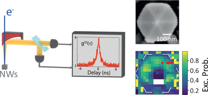
Cathodoluminescence (CL) imaging spectroscopy provides two-dimensional optical excitation images of photonic nanostructures with a deep-subwavelength spatial resolution. So far, CL imaging was unable to provide a direct measurement of the excitation and emission probabilities of photonic nanostructures in a spatially resolved manner. Here, we demonstrate that by mapping the cathodoluminescence autocorrelation function g(2) together with the CL spectral distribution the excitation and emission rates can be disentangled at every excitation position. We use InGaN/GaN quantum wells in GaN nanowires with diameters in the range 200–500 nm as a model system to test our new g(2) mapping methodology and find characteristic differences in excitation and emission rates both between wires and within wires. Strong differences in the average CL intensity between the wires are the result of differences in the emission efficiencies. At the highest spatial resolution, intensity variations observed within wires are the result of excitation rates that vary with the nanoscale geometry of the structures. The fact that strong spatial variations observed in the CL intensity are not only uniquely linked to variations in emission efficiency but also linked to excitation efficiency has profound implications for the interpretation of the CL data for nanostructured geometries in general.
Keywords: Semiconductor, spectroscopy, cathodoluminescence, autocorrelation function, SEM, nano-optics
Cathodoluminescence (CL) spectroscopy is a well-known technique for the optical characterization of nanomaterials.1−10 In CL, a high-energy electron beam in an electron microscope is raster-scanned over the surface of a material, and both the secondary electron (SE) emission and the emitted light are simultaneously collected.11−13 In this way, the obtained CL emission pattern can be correlated with the geometry of the sample. Due to the small electron-beam interaction volumes that are attainable, CL spectroscopy can provide optical excitation maps with a deep-subwavelength spatial resolution.
The intensity of the detected CL emission at every electron-beam position is determined both by the local excitation efficiency of the radiating material by the incoming electron and the emission efficiency of the material itself.11,12 While conventional CL spectroscopy yields optical spectra in a quantitative way, it does not enable separation of the excitation and emission rates. In SEM, the excitation efficiency depends strongly on the 3D geometry, e.g., edges, corners, facets, stratification, and depth variations.14 This implies that interesting features in the emission efficiency, connected to the intrinsic properties of the material, often remain hidden in conventional CL mapping. Until now, the excitation efficiency has to be retrieved independently using 3D beam-tracing Monte Carlo simulations that have to take into account the full sample geometry and all carrier diffusion processes.15−17 However, this approach is time-consuming and relies on a large number of assumptions, in particular in the carrier dynamics. Furthermore, retrieving the full 3D geometry requires advanced (destructive) cross-sectional imaging using focused ion beam milling, for example. Therefore, in order to obtain a fundamental understanding of the intrinsic properties of optical nanostructures, it is essential to obtain information on the excitation and emission rates in a direct manner. Such data are invaluable to obtain insight into material quality and (in)homogeneity of optical nanostructures, essential parameters in device characterization and optimization.
In this Letter, we introduce a new technique in which we measure the spatially resolved CL autocorrelation function in a scanning electron microscope (SEM) to resolve this problem. The autocorrelation function g(2)(τ) describes the probability for two emitted photons to be separated by a certain time delay τ.18 For example, when a single electron excites a semiconductor quantum well (QW), a packet composed of multiple photons is emitted that leads to a peak at τ = 0 in the autocorrelation function (g(2)(0) ≫ 1).19−21 It has been shown that the precise characteristics of this photon bunching peak depend only on the electron current, the lifetime of the emitter τe, and the probability of excitation by the electron γ, which can be strongly geometry dependent as mentioned above.19−21 If the electron current decreases, the time between two electrons increases, resulting in a better separation of the photon bunches and thus stronger bunching (g(2)(0) increases). Following the same reasoning, if τe decreases, for a given current, the separation between photon bunches increases resulting in stronger bunching (g(2)(0) increases). Finally, if the excitation efficiency γ decreases, the time between two incoming electrons interacting with the sample effectively increases (similar to the effect of a reduced current) leading to a stronger bunching (g(2)(0) increases). As the beam current is known for a given data acquisition, τe and γ can be determined independently from the g(2) data.20 In this way, the excitation efficiency γ can be extracted for any position on the sample without a priori knowledge on the sample geometry, a major advantage in complex 3D semiconductor geometries as we will show.
Here, we present spectroscopy and g(2) maps of semiconductor nanostructures and by combining these data we derive spatially resolved information on the relative excitation and emission rates without a priori knowledge of the structure. We define the emission efficiency as the number of photons emitted into the upper hemisphere per interacting electron; it is determined by the intrinsic emission efficiency and the outcoupling efficiency. (See the Supporting Information, section 4, for details.) To do so, we raster-scan the electron beam over the sample and record the SE signal together with the CL spectrum or the g(2)(τ) distribution for each excitation position (x,y). We investigate InGaN quantum wells (QWs) embedded in GaN nanowires (NWs) because as we will show these nanostructures exhibit characteristic differences in excitation and emission efficiency that vary at subwavelength scales.
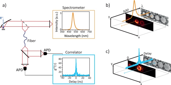
Figure 1 shows a schematic view of the measurement setup. In Figure 1a, the CL collection setup is sketched both for CL spectroscopy and g(2) analysis. Figure 1b shows the spectral data cube, in which a spectrum is collected at every (x,y) pixel; a cross section of the data is shown representing a spatial CL intensity map at a given wavelength. Similarly, in Figure 1c, the autocorrelation time histogram data cube is shown with a cross section representing the histogram amplitude at τ = 0 for every pixel. To obtain a g(2) curve at each (x,y) position, the data is normalized by the average number of counts per time bin recorded at a large delay. (See the Supporting Information, section 2.)
Figure 1.
Schematic view of the CL spectroscopy/g(2) experiment on InGaN/GaN QW NWs. (a) Layout of the measurement setup; the light emitted by the sample is collected by a parabolic mirror and sent to either a spectrometer (top path) to record the spectrum or a Hanbury Brown and Twiss (HBT) interferometer, in which the delay between photon detection in each of the two avalanche photodiodes (APD) is recorded by a correlator. A time histogram is built from which the autocorrelation function g(2)(τ) is derived. (b) Spectral data cube containing a CL spectrum and the SE intensity at each pixel. (c) Data cube containing autocorrelation time histogram.
We investigate InGaN/GaN QWs nanowires grown by radio frequency plasma-assisted molecular beam epitaxy (MBE) on selective-area growth patterns defined using a Ti mask.22 The NWs were grown on an n-type GaN template on a sapphire substrate. In this growth process, the size and surface morphology of the nanowires can be precisely controlled by varying the nanopatterns on the growth mask.23 The top-view SEM image in Figure 2b shows five hexagonally shaped NWs with diameters in the range ∼200–500 nm. (For details, see the Supporting Information, section 1.) Five vertically aligned InGaN/GaN quantum wells are incorporated in each GaN NW. A cross-section of the smallest NW is shown in Figure 2a. The NW arrays studied in this work are surrounded by smaller randomly oriented GaN NWs that are nucleated and grew on top of the Ti mask. (See the cross-section in Figure 2a.) All CL experiments were performed at an electron energy of 5 keV at room temperature. The CL spectra averaged over the projected area of each NW are shown in Figure 2e. Figure 2c shows a false-color RGB map, which is constructed by dividing the wavelength range from 400 to 550 nm in blue (400–450 nm), green (450–500 nm), and red (500–550 nm) color channels, respectively. This map clearly visualizes spectral variations for different positions. Emission is visible for excitation around the NWs as well, which we attribute to indirect excitation of the InGaN/GaN NWs by secondary and backscattered electrons produced by the interaction with the small GaN NWs surrounding the NWs. (See Figure 2a.) The CL data have been calibrated using the method described in refs (20) and (24) using the known electron current (52 pA) as the input, yielding the average number of photons emitted per incident electron per unit bandwidth.
Figure 2.
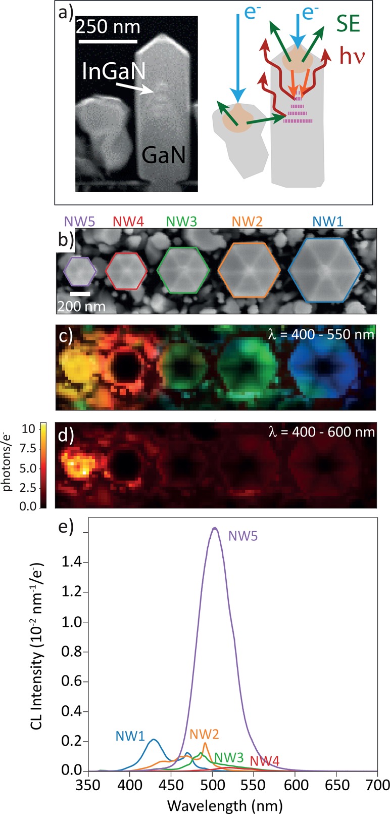
Cathodoluminescence for InGaN/GaN QWs embedded in GaN NWs. (a) (Left) Cross section of a NW similar to NW5 and (right) schematic view of the excitation mechanisms that lead to CL emission (hν) either through direct excitation of the NW or by secondary electrons (SE) originating from surrounding NWs. (b) SEM image taken together with the CL data set shown in parts c, d, and e. (c) False-color RGB image of the CL data cube. The spectra are separated in 3 sections (in the range from 400 to 550 nm), which are binned such that the total intensity in these spectral regions defines an RGB code for every position. (d) CL intensity (photons per incident electron) integrated over the 400–600 nm wavelength range, corresponding to the filter used in the g(2) measurements. The color scale indicates the average number of photons emitted into the upper angular hemisphere (zenithal angle θ between 0° and 90°, where θ = 0° corresponds to the surface normal) per incoming electron within this spectral bandwidth. (e) CL spectra for the five NWs averaged over the full NW area.
In order to determine if the intensity variations in Figure 2e originate from variations in excitation or emission efficiencies, we perform g(2) measurements across the NW array shown in Figure 2 using a pixel size of 50 × 50 nm2 and a collection bandwidth from 400 to 600 nm. The integration time is 30 s per pixel, and drift correction was carried out using the SE image collected on a specified reference region. For each pixel, g(2)(τ) data were fitted with
| 1 |
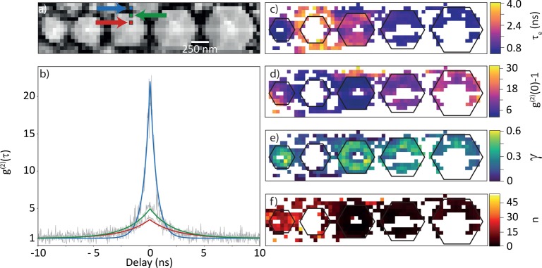
with g0 as the amplitude of the g(2) peak at τ = 0 and τe as the lifetime of the excited state. The g(2) function is mostly sensitive to the main decay component.19−21 Here, we fit the g(2) function with a single exponential, which allows us to accurately retrieve the shape of the g(2) curve even though the system in reality possibly exhibits a more complex multiexponential25,26 or nonexponential decay.27 (See section 3 of the Supporting Information.) Figure 3b shows three characteristic g(2) measurements taken on or near NW3. Fits of eq 1 are also shown and represent the data well. The strong peaks at g(2)(0) reflect bunching in the photon emission, as was observed before in both TEM and SEM studies,19−21 and result from the generation of multiple excitations by a single incident electron. The red and green curves in Figure 3b are taken on NW3 and show a similar bunching (g(2)(0)-1 = 3–4) and lifetime (τe = 2.7 ± 0.2 and 2.1 ns ± 0.2 ns, respectively). The lifetimes of InGaN QW emission are known to depend strongly on the exact composition, defect structure, and optical environment.28−30 The blue curve, taken on the GaN substrate next to NW3, shows a much shorter lifetime (τe = 600 ± 130 ps) and much stronger bunching. We attribute the latter to the shorter lifetime and a smaller excitation probability due to the indirect excitation through secondary and backscattered electrons.
Figure 3.
g(2) maps for the NW array displayed in Figure 2. (a) SE intensity recorded together with the g(2) data set. The g(2) data recorded at three colored squares in part a as indicated by the arrows are shown in part b as well as the fits to eq 1 (colored lines). (c–f) Maps of lifetime τe, amplitude g(2)(0)-1, probability of excitation of the QWs γ, and average number of photons emitted per electron interacting with the QWs (n). The contours of the NWs are indicated by black lines.
Figure 3c,d show maps of the fitted values of g(2)(0) (plotted as g(2)(0)-1) and τe for all scanned pixels for the five NWs. On some pixels, the signal-to-noise ratio was too low to accurately fit the g(2) data. (See the Supporting Information.) In this case, the pixels are displayed as white in the maps. Next, using the statistical model described in ref (20), we derive the probability of excitation γ, defined as the fraction of electrons that excite the optically active regions (QWs), for each pixel. The input parameters for this analysis are the beam current (52 pA), the lifetime τe, and the amplitude g(2)(0)-1. (See section 2 in the Supporting Information for details.) This statistical analysis uniquely defines the probability of excitation γ without a priori knowledge of the structure itself.
The 2D map of the excitation probability γ is shown in Figure 3e. For the pixels where the g(2) data could be fitted, the excitation efficiency is quite similar for the different NWs (γ ≈ 0.35), which means that the electrons excite the different NWs at a similar rate. (See section 2 in the Supporting Information for more details.) This is consistent with the fact that the QWs are located at approximately the same depth below the p-doped GaN segments for all NWs.15 (See section 1 of the Supporting Information.) Finally, by combining the data in Figures 2d and 3e, we can derive the average number of photons emitted per electron exciting the QW at every pixel (n, Figure 3f). The map then represents the combined effect of internal emission efficiency and outcoupling efficiency per QW excitation, which presents an important metric for device characterization. In this analysis, the SE images of Figures 2b and 3a are used to spatially correlate the spectroscopy and g(2) data sets, which are taken in separate experimental runs. (See the Supporting Information.) This analysis shows that the higher CL intensity observed for NW5 in Figure 2d is correlated with a higher number of photons emitted per exciting electron (Figure 3f), indicating that the difference in CL intensity between the NWs originates from a difference in the relative emission efficiency rather than the excitation efficiency. Analysis of CL spectroscopy data on 12 NW arrays shows that the smallest NW is not always the brightest one. (See the Supporting Information, Figure S5.) The differences are attributed to minor variations in the epitaxial growth conditions at the different arrays leading to different minority carrier recombination rates in the NWs.31−33
Next, we use the same analysis method to investigate the dark hexagonal line pattern observed within individual NWs (such as in Figure 2c), which coincides with the 6-fold pyramidal faceting at the top surface. Using a different NW array than the one described above, but with identical NW geometry (SE image in Figure 4b), we collect the CL images shown in Figure 4c,d. In the analysis, we will focus on the bright NW3 at the center that has an almost constant CL spectral shape across the NW (homogeneous green profile in Figure 4c). The spectral intensity map for the 400–600 nm range clearly shows the dark hexagonal pattern as well (Figure 4d).
Figure 4.
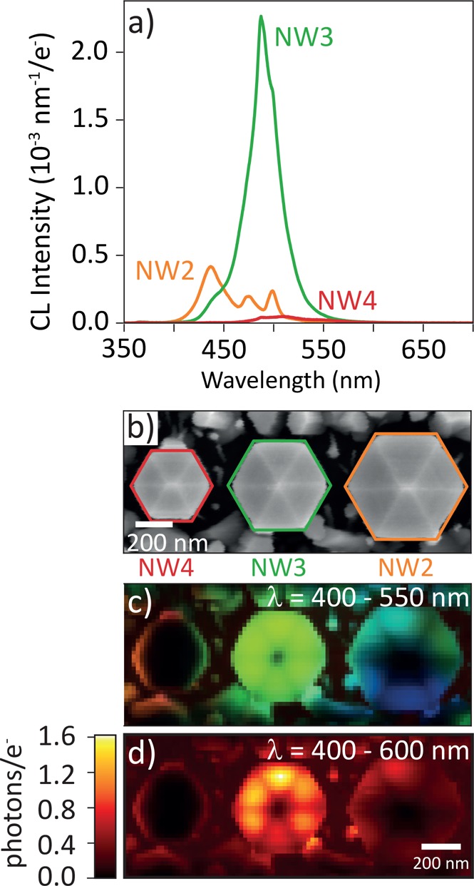
High-resolution CL spectroscopy on three NWs. (a) Averaged spectra for the three NWs shown in the SE image in part b. (c) RGB image of CL spectra, false-color coded from 400 to 550 nm. (d) CL intensity map (photons per incoming electron) for the range from 400 to 600 nm.
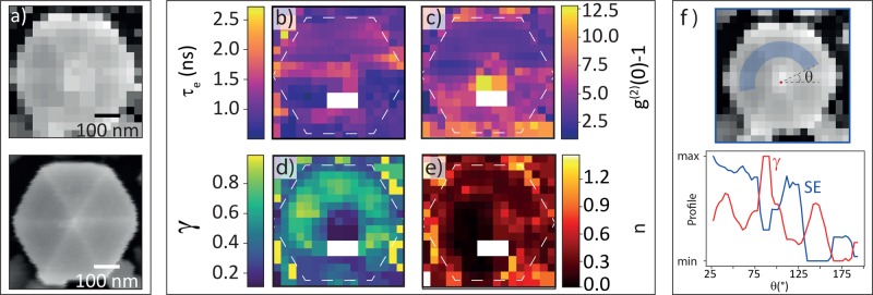
The g(2) map for this NW is shown in Figure 5a, taken using a pixel size of 30 × 30 nm2. Using the same analysis as described above, the fit results for τe and g(2)(0) are shown in Figure 5b,c. In order to fit g(2) for the broadest possible spatial range, in some cases, data arrays of (2 × 2) pixels were summed to increase the signal-to-noise ratio. The corresponding SEM image is shown in Figure 5a (top), where larger pixels are visible in the lower part. In the same way as described above, we derive a spatial map of the excitation efficiency γ (Figure 5d). In this image, the hexagonal pattern of dark lines corresponding to the edges between facets is clearly visible. This is further emphasized by the azimuthal line profile shown in Figure 5f, revealing that the probability of exciting the QWs varies strongly within the NW. It is known that in CL maps the signal can drop near sharp edges and vertices as there is a higher probability for electrons to escape from the structure, thereby limiting the excitation probability (γ).14,34 Conversely, the SE signal is expected to be elevated in such places due to this higher escape probability, a common occurrence in SEM. (See the line profile in Figure 5f.) Indeed, the SE signal in Figure 5a (bottom) is strongest at the apexes where the edges join. By combining the data in Figures 4d and 5d, we derive a spatial map of the average number of photons generated per electron exciting the QWs (n, Figure 5e). In this map, the hexagonal pattern has disappeared, indicating that this feature indeed is related to the excitation mechanism. The remaining intensity variation observed in Figure 5e then reflects variations in the emission efficiency, which are not visible in the raw spectral CL images.
Figure 5.
g(2) maps of NW3 of Figure 4. (a) SE images, taken together with the g(2) data set (top) and the CL data set (bottom). (b, c) Map of lifetime τe and g(2)(0)-1 derived from g(2)(τ) fits. (d) Map of the fraction of incoming electrons that excites the QWs (γ). (e) Map of the average number of photons generated per electron interacting with the QWs n. (f) Line profile along the blue arc on the SE image and the γ map. The data are scaled to show the range defined by the minimum and maximum value of SE data and γ map (d). The intensity maxima in the γ map correspond to minima on the SE image and vice versa.
In conclusion, we have shown that by combining measurements of the spatial distribution of CL spectra and the g(2)(τ) photon correlation function the excitation and emission efficiencies in semiconductor nanostructures can be disentangled. The high spatial resolution of CL enables the separation of the excitation and emission efficiencies at a deep-subwavelength scale. We find that in the GaN NWs the CL intensity difference between NWs is the result of a difference in the emission efficiency. In contrast, CL intensity variations within individual NWs are dominated by sample geometry-induced variations in the electron excitation efficiency. This new technique can now be used to unravel excitation and emission processes in a broad range of optical nanostructures, for example, (faceted) nanowires,35 semiconductor platelets,36 core–shell structures,37 and stratified heterostructures/multilayer stacks.38 Similarly, g(2) mapping can be used to characterize single-photon sources such as diamond NV centers or semiconductor quantum dots at the nanoscale.
Acknowledgments
This work is part of the research program of the “Nederlandse organisatie voor Wetenschappelijk Onderzoek” (NWO). It is also funded by the European Research Council (ERC). Y.H.R. and Z.M. thank the support from the Natural Sciences and Engineering Research Council of Canada (NSERC) and National Science Foundation (Grant ECCS-1709207).
Supporting Information Available
The Supporting Information is available free of charge on the ACS Publications website at DOI: 10.1021/acs.nanolett.7b04891.
Nanowire geometry and description of the sample fabrication, g(2) fitting procedure and normalization, 3D Monte Carlo based model, method to derive the efficiency map, and CL data on 12 NW arrays (PDF)
The authors declare the following competing financial interest(s): A.P. is co-founder and co-owner and T. C. is employee of Delmic BV, a startup company that produces a commercial cathodoluminescence system that was used in this work.
Supplementary Material
References
- Coenen T.; Haegel N. M. Appl. Phys. Rev. 2017, 4, 031103. 10.1063/1.4985767. [DOI] [Google Scholar]
- Tizei L. H. G.; Kociak M. Phys. Rev. Lett. 2013, 110, 153604. 10.1103/PhysRevLett.110.153604. [DOI] [PubMed] [Google Scholar]
- Edwards P. R.; Martin R. W. Semicond. Sci. Technol. 2011, 26, 064005. 10.1088/0268-1242/26/6/064005. [DOI] [Google Scholar]
- Merano M.; Sonderegger S.; Crottini a.; Collin S.; Renucci P.; Pelucchi E.; Malko a.; Baier M. H.; Kapon E.; Deveaud B.; Ganière J.-D. Nature 2005, 438, 479–482. 10.1038/nature04298. [DOI] [PubMed] [Google Scholar]
- Sonderegger S.; Feltin E.; Merano M.; Crottini a.; Carlin J. F.; Sachot R.; Deveaud B.; Grandjean N.; Ganière J. D. Appl. Phys. Lett. 2006, 89, 232109. 10.1063/1.2397562. [DOI] [Google Scholar]
- Zagonel L. F.; Mazzucco S.; Tencé M.; March K.; Bernard R.; Laslier B.; Jacopin G.; Tchernycheva M.; Rigutti L.; Julien F. H.; Songmuang R.; Kociak M. Nano Lett. 2011, 11, 568–573. 10.1021/nl103549t. [DOI] [PubMed] [Google Scholar]
- Atre A. C.; Brenny B. J. M.; Coenen T.; García-Etxarri A.; Polman A.; Dionne J. a. Nat. Nanotechnol. 2015, 10, 429–436. 10.1038/nnano.2015.39. [DOI] [PubMed] [Google Scholar]
- Osorio C. I.; Coenen T.; Brenny B. J. M.; Polman A.; Koenderink A. F. ACS Photonics 2016, 3, 147–154. 10.1021/acsphotonics.5b00596. [DOI] [Google Scholar]
- Latzel M.; Büttner P.; Sarau G.; Höflich K.; Heilmann M.; Chen W.; Wen X.; Conibeer G.; Christiansen S. H. Nanotechnology 2017, 28, 055201. 10.1088/1361-6528/28/5/055201. [DOI] [PubMed] [Google Scholar]
- Jacopin G.; Rigutti L.; Largeau L.; Fortuna F.; Furtmayr F.; Julien F. H.; Eickhoff M.; Tchernycheva M. J. Appl. Phys. 2011, 110, 064313. 10.1063/1.3638698. [DOI] [Google Scholar]
- Holt D. B.Cathodoluminescence Microscopy of Inorganic Solids; Springer: Berlin, Germany, 1990; Vol. 49. [Google Scholar]
- García de Abajo J. Rev. Mod. Phys. 2010, 82, 209. 10.1103/RevModPhys.82.209. [DOI] [Google Scholar]
- Edwards P. R.; Martin R. W. Semicond. Sci. Technol. 2011, 26, 064005. 10.1088/0268-1242/26/6/064005. [DOI] [Google Scholar]
- Ledig J.; Wang X.; Fündling S.; Schuhmann H.; Seibt M.; Jahn U.; Wehmann H. H.; Waag A. Phys. Status Solidi A 2016, 213, 11–18. 10.1002/pssa.201532485. [DOI] [Google Scholar]
- Demers H.; Poirier-Demers N.; Couture A. R.; Joly D.; Guilmain M.; De Jonge N.; Drouin D. Scanning 2011, 33, 135–146. 10.1002/sca.20262. [DOI] [PMC free article] [PubMed] [Google Scholar]
- Demers H.; Poirier-Demers N.; Phillips M. R.; de Jonge N.; Drouin D. Microsc. Microanal. 2012, 18, 1220. 10.1017/S1431927612013414. [DOI] [PubMed] [Google Scholar]
- Phang J. C. H.; Pey K. L.; Chang D. S. H. IEEE Trans. Electron Devices 1992, 39, 782–791. 10.1109/16.127466. [DOI] [Google Scholar]
- Hanbury Brown R.; Twiss R. Q. J. Astrophys. Astron. 1994, 15, 13–19. 10.1007/BF03010401. [DOI] [Google Scholar]
- Meuret S.; Tizei L. H. G.; Cazimajou T.; Bourrellier R.; Chang H. C.; Treussart F.; Kociak M. Phys. Rev. Lett. 2015, 114, 197401. 10.1103/PhysRevLett.114.197401. [DOI] [PubMed] [Google Scholar]
- Meuret S.; Coenen T.; Zeijlemaker H.; Latzel M.; Christiansen S.; Conesa-Boj S.; Polman A. Phys. Rev. B: Condens. Matter Mater. Phys. 2017, 96, 035308. 10.1103/PhysRevB.96.035308. [DOI] [Google Scholar]
- Meuret S.; Tizei L. H. G.; Auzelle T.; Songmuang R.; Daudin B.; Gayral B.; Kociak M. ACS Photonics 2016, 3, 1157–1163. 10.1021/acsphotonics.6b00212. [DOI] [Google Scholar]
- Ra Y. H.; Wang R.; Woo S. Y.; Djavid M.; Sadaf S. M.; Lee J.; Botton G. A.; Mi Z. Nano Lett. 2016, 16, 4608–4615. 10.1021/acs.nanolett.6b01929. [DOI] [PubMed] [Google Scholar]
- Ra Y.; Rashid R. T.; Liu X.; Lee J.; Mi Z. Adv. Funct. Mater. 2017, 27, 1702364. 10.1002/adfm.201702364. [DOI] [Google Scholar]
- Brenny B. J. M.; Coenen T.; Polman A. J. Appl. Phys. 2014, 115, 244307. 10.1063/1.4885426. [DOI] [Google Scholar]
- Morel A.; Lefebvre P.; Kalliakos S.; Taliercio T.; Bretagnon T.; Gil B. Phys. Rev. B: Condens. Matter Mater. Phys. 2003, 68, 45331. 10.1103/PhysRevB.68.045331. [DOI] [Google Scholar]
- Brosseau C.-N.; Perrin M.; Silva C.; Leonelli R. Phys. Rev. B: Condens. Matter Mater. Phys. 2010, 82, 85305. 10.1103/PhysRevB.82.085305. [DOI] [Google Scholar]
- Cardin V.; Dion-Bertrand L. I.; Grégoire P.; Nguyen H. P. T.; Sakowicz M.; Mi Z.; Silva C.; Leonelli R. Nanotechnology 2013, 24, 045702. 10.1088/0957-4484/24/4/045702. [DOI] [PubMed] [Google Scholar]
- Nguyen H. P. T.; Djavid M.; Woo S. Y.; Liu X.; Connie A. T.; Sadaf S.; Wang Q.; Botton G. A.; Shih I.; Mi Z. Sci. Rep. 2015, 5, 7744. 10.1038/srep07744. [DOI] [PMC free article] [PubMed] [Google Scholar]
- Deshpande S.; Frost T.; Yan L.; Jahangir S.; Hazari A.; Liu X.; Mirecki-Millunchick J.; Mi Z.; Bhattacharya P. Nano Lett. 2015, 15, 1647–1653. 10.1021/nl5041989. [DOI] [PubMed] [Google Scholar]
- Guo W.; Zhang M.; Banerjee A.; Bhattacharya P. Nano Lett. 2010, 10, 3355–3359. 10.1021/nl101027x. [DOI] [PubMed] [Google Scholar]
- Yamamoto S.; Zhao Y.; Pan C. C.; Chung R. B.; Fujito K.; Sonoda J.; DenBaars S. P.; Nakamura S. Appl. Phys. Express 2010, 3, 122102. 10.1143/APEX.3.122102. [DOI] [Google Scholar]
- Zhang M.; Bhattacharya P.; Guo W. Appl. Phys. Lett. 2010, 97, 011103. 10.1063/1.3460921. [DOI] [Google Scholar]
- Tourbot G.; Bougerol C.; Grenier A.; Den Hertog M.; Sam-Giao D.; Cooper D.; Gilet P.; Gayral B.; Daudin B. Nanotechnology 2011, 22, 075601. 10.1088/0957-4484/22/7/075601. [DOI] [PubMed] [Google Scholar]
- Tchernycheva M.; Neplokh V.; Zhang H.; Lavenus P.; Rigutti L.; Bayle F.; Julien F. H.; Babichev A.; Jacopin G.; Largeau L.; Ciechonski R.; Vescovi G.; Kryliouk O. Nanoscale 2015, 7, 11692–11701. 10.1039/C5NR00623F. [DOI] [PubMed] [Google Scholar]
- Goh W. H.; Patriarche G.; Bonanno P. L.; Gautier S.; Moudakir T.; Abid M.; Orsal G.; Sirenko A. A.; Cai Z. H.; Martinez A.; Ramdane A.; Le Gratiet L.; Troadec D.; Soltani A.; Ougazzaden A. J. Cryst. Growth 2011, 315, 160–163. 10.1016/j.jcrysgro.2010.08.053. [DOI] [Google Scholar]
- Mukherjee S.; Nateghi N.; Jacobberger R. M.; Bouthillier E.; de la Mata M.; Arbiol J.; Coenen T.; Cardinal D.; Levesque P.; Desjardins P.; Martel R.; Arnold M. S.; Moutanabbir O. Adv. Funct. Mater. 2018, 28, 1705592. 10.1002/adfm.201705592. [DOI] [Google Scholar]
- Lauhon L. J.; Gudiksen M. S.; Wang D.; Lieber C. M. Nature 2002, 420, 57–61. 10.1038/nature01141. [DOI] [PubMed] [Google Scholar]
- Latzel M.; Büttner P.; Sarau G.; Höflich K.; Heilmann M.; Chen W.; Wen X.; Conibeer G.; Christiansen S. H. Nanotechnology 2017, 28, 055201. 10.1088/1361-6528/28/5/055201. [DOI] [PubMed] [Google Scholar]
Associated Data
This section collects any data citations, data availability statements, or supplementary materials included in this article.


