Abstract
2D layered materials (2DLMs), together with their heterostructures, have been attracting tremendous research interest in recent years because of their unique physical and electrical properties. A variety of circuit elements have been made using mechanically exfoliated 2DLMs recently, including hard drives, detectors, sensors, and complementary metal oxide semiconductor field‐effect transistors. However, 2DLM‐based amplifier circuit elements are rarely studied. Here, the integration of 2DLMs with 3D bulk materials to fabricate vertical junction transistors with current amplification based on a MoS2/GaTe heterostructure is reported. Vertical junction transistors exhibit the typical current amplification characteristics of conventional bulk bipolar junction transistors while having good current transmission coefficients (α ∼ 0.95) and current gain coefficient (β ∼ 7) at room temperature. The devices provide new attractive prospects in the investigation of 2DLM‐based integrated circuits based on amplifier circuits.
Keywords: 2D materials, bipolar junction transistor, current amplification, van der Waals heterostructure
Since the basic concept of the bipolar junction transistor (BJT) was patented by Shockley in 1948 and experimentally realized in 1951,1 BJTs have launched the microelectronics revolution that led to the Information Age. Until the widespread emergence of complementary metal oxide semiconductor (CMOS) technology in the 1980s, the BJT was the dominant semiconductor technology in microelectronic manufacturing. Compared to CMOSs, BJTs exhibit a higher output current and larger transconductance per unit length, faster switching speeds (particularly under capacitive loading), and excellent properties for many analog and amplifier applications.2, 3 Thus, this creative three‐terminal (emitter–base collector) device, which acts like a transistor, can be used to build a wide variety of electronic circuits. Modern applications of BJTs have changed; the most notable include high‐speed digital integrated circuits in mainframe computers, precision analog circuits, and amplifier circuits found in radio communications systems. Hence, BJTs still occupy a significant portion of the global semiconductor market. Although the primary drawbacks of BJT circuits (compared to CMOS) include larger direct current (DC) power dissipation and fabrication complexity, BJTs remain the first choice to meet high‐frequency requirements and fast switching speeds. BJTs generally consist of two back‐to‐back pn junctions (p–n–p or n–p–n, depending on the doping polarity). To achieve its high‐frequency and high‐amplification characteristics, the intermediate n or p region should be infinitesimally thin. However, the ultrathin base region is difficult to produce using the conventional processing methods because conventional bulk semiconductors (e.g., Si, Ge, and III–IV materials) limit the current amplification. Therefore, we adopted 2D materials as the base region, which can be as thin as an atom.
The discovery of graphene, one of the most famous 2D layered materials (2DLMs), has been a strong boost for world‐wide research of 2DLMs with diverse electronic properties over the past decade.4, 5, 6, 7, 8, 9, 10, 11, 12, 13 Because the thickness of a 2DLM monolayer can be as thin as an atom and the surface is free of dangling bonds, 2DLMs surpass typical nanostructures that are plagued by dangling bonds and trap states. Neighboring 2DLM layers usually interact with each other by van der Waals force,14, 15 which allows for the integration of highly disparate materials with crystal lattice mismatching. There is considerable freedom in integrating 2DLMs and various nanoscale materials to create a set of diverse van der Waals heterostructures (vdWHs), with functions that could not be achieved previously. Until now, in addition to basic circuit elements such as transistors and CMOSs16, 17, 18, 19 based on mechanically exfoliated 2DLMs, more complex circuits have also been achieved recently that were based on vdWHs,20, 21, 22, 23, 24 such as memories, detectors, and sensors. Nevertheless, as an important part of integrated circuits, 2DLM‐based amplifier circuits have rarely been studied.
Considering the difficulty doping in 2DLMs and the small current of 2DLMs devices, the integration of 3D materials and 2DLMs with different polarity can overcome most challenges. In this work, we report the preparation and characterization of vertical bipolar junction transistors assembled using a GaTe/MoS2 heterostructure. MoS2 is an ideal material for the base because of its excellent electrical performance.25, 26, 27, 28, 29 Because the requirement for the emitter region is to provide a large number of holes to inject into the base region in the amplification process, the highly p‐doped GaTe is ideal for the emitter region. Thus, the GaTe–MoS2 interface acts as a base–emitter junction. The slightly p‐doped Si acts as the collector, and the MoS2–Si interface acts as the base–collector junction. The doping for different regions of this vertical heterostructure bipolar junction transistor (HBT) is more precise than electrostatic doping with multigate control,30 which requires at least six voltages. Thus, electrostatic doping with multigate control is not good for practical applications or for the fabrication of integrated circuits due to its buried gates. Instead, the vertical HBT exhibits typical characteristic curves (i.e., conventional post‐Si BJT), and the current gain coefficient β can reach 7 at room temperature.
Vertical bipolar junction transistors were fabricated by transferring mechanically exfoliated GaTe and MoS2 thin films sequentially onto a slightly p‐doped Si substrate to form a GaTe/MoS2/Si sandwich structure. The fabrication process flow diagram is shown in Figure 1 . The optical measurement of the device is shown in Figure 2 a, with the circled regions (red and blue) representing MoS2 and GaTe flakes, respectively. Both of the MoS2 and GaTe flakes are layered materials stacked by van der Waals force; thus, few‐layer materials can be peeled off from their bulk states, along the van der Waals gaps. Figure 2b shows a cross‐section schematic diagram of the device, the device structure, and the formation of two van der Waals heterostructures. Figure 2c shows the typical photoluminescence (PL) spectra for the GaTe–MoS2 overlapped area, individual MoS2, and individual GaTe under 532 nm laser excitation. Under strong laser intensity, individual MoS2 show mild PL signals of both the A‐excitonic peak at 1.81 eV and B‐excitonic peak at 1.98 eV. We note that the 1.4 eV peak associated with the indirect bandgap of MoS2 could not be observed. There might be three possible origins: the hot luminescence (A and B excitons) peaks induced by strong laser excitation,31 defect‐weakening phonon‐assisted indirect emission process,32 or interlayer coupling influencing the conduction band minimum (CBM) and valence band maximum (VBM) in such a way as to halt indirect emission line.33 Similarly, GaTe flakes have an emission line at 1.96 eV. At the overlapping area, all peaks appear at 1.81, 1.98, and 1.96 eV. The atomic force microscopy measurement is also shown in Figure 2d,e. The uniform contrast observed in the overlapping region demonstrates good contacts between the two flakes and the Si substrate. Figure S1 in the Supporting Information shows the Raman spectroscopic measurements at different positions of the Si substrate. Well‐developed peaks indicate that the MoS2 and GaTe flakes are well‐maintained on the Si surface after the transfer process. The corresponding spatially resolved Raman maps of GaTe (at Raman shift of 145 cm−1) and MoS2 (at Raman shift of 408 cm−1) are shown in Figure 2g,h. Additionally, the cross‐sectional TEM image and EDS mapping of the as‐fabricated vertical bipolar junction transistor are shown in Figure 2f,i, respectively.
Figure 1.
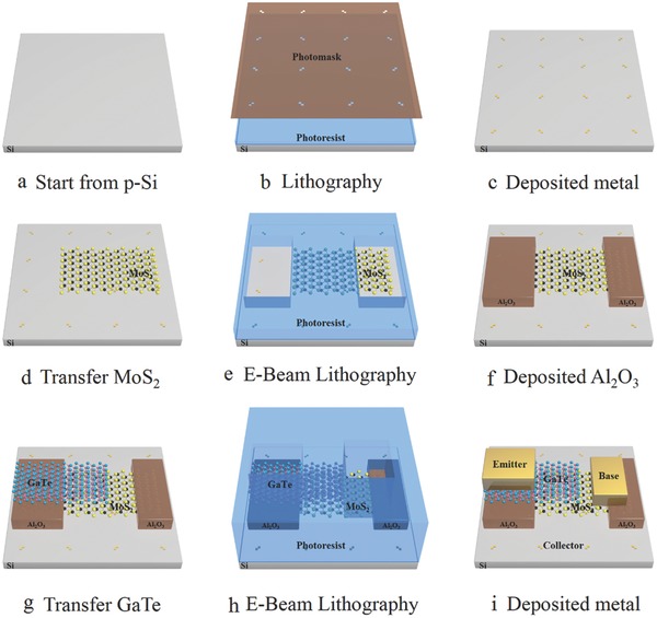
Schematic diagram showing fabrication process flow of the vertical bipolar junction transistor.
Figure 2.
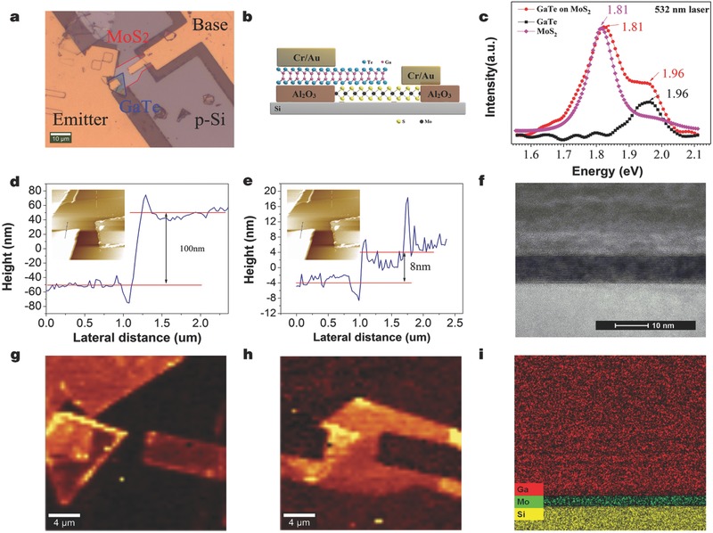
a) The optical microscopy of the bipolar junction transistor device showing the base and emitter contacts. Scale bar: 10 µm. b) Schematic diagram of the structure for the bipolar junction transistor. c) Typical photoluminescence spectra of an individual MoS2, an individual GaTe and a MoS2/GaTe heterostructure. d,e) Height profiles of the device. A step height of GaTe ≈100 nm and MoS2 ≈8 nm is measured. Inset: AFM image of the device. g,h) Spatially resolved Raman maps for the GaTe (Raman shift at 145 cm−1) and the MoS2 (Raman shift at 408 cm−1). f) Cross‐sectional TEM images of the device. Scale bar is 2 nm. i) EDS mapping of the device.
With the well‐defined p‐type characteristics of GaTe and n‐type characteristics of MoS2 (Figure S2, Supporting Information), the device exhibits typical characteristics of a p–n–p HBT. Prior to investigating the electrical characteristics of the HBT, electrical transport properties of p‐Si/MoS2 and GaTe/MoS2 heterostructures were characterized to ensure the p–n diode was achieved from the start. The electrical characterizations of the heterostructures were performed via a two‐terminal configuration, using the base–emitter or base–collector contacts, as shown in Figure 3 . Typical current–voltage (I–V) characteristics, under varying voltage, of p‐Si/MoS2 heterostructure is shown in Figure 3a. Clear current rectification behavior was observed in the I–V plots of p‐Si/MoS2 heterostructures. This suggests that the current can pass through the device only when the p‐type Si is positively biased. The observations of the current rectification demonstrated a p–n diode within the p‐Si/MoS2 vertical heterostructures. When V was in range of ±1 V, the p‐Si/MoS2 heterostructures showed a rectification ratio of over 700. The I–V characteristics of the vertical GaTe/MoS2 heterostructures exhibited typical rectifying behavior with an on‐off current ratio of ≈1800 when V was within the ±1 V range (Figure 3b). Under a positive bias voltage, the built‐in potential at the interface between GaTe and MoS2 was reduced. The electrons could then be transported across the layers easily, resulting in a large on‐state current. Similarly, under a negative bias voltage, the built‐in potential was also much greater and resulted in a small off‐state current. Importantly, the ideality factor n has also been derived via the semilogarithm I–V plot data. By using the slope, the following equation (Calculation details described in Section 3 of the Supporting Information) determines the ideality factor n
| (1) |
where q is the elementary charge, k is the Boltzmann constant, and T is the temperature. The ideality factor of p‐Si/MoS2 heterostructures device is calculated as 1.178. However, the value of n obtained in MoS2/GaTe heterostructures device is 1.62. The deviation from the ideal diode behavior (n = 1) can be attributed to the additional series resistance in the device in the high forward bias region;34 it can also result from the presence of interfacial defects at the junction.35
Figure 3.
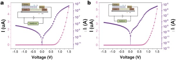
Current versus bias voltage characteristic of a) MoS2/p‐Si junction and b) GaTe/MoS2 junction. The insets show the measurement schematic diagrams for p‐silicon/MoS2 and GaTe/MoS2 junction, respectively.
For the fabricated p–n–p transistor with a common‐base configuration, a set of output characteristics are shown in Figure 4 a. The output characteristic curves indicate the variation in the collector current (I C) with a changing collector–base voltage (V CB) when the emitter current (I E) was kept constant. I E changed from 0 to 14 µA with a step size of 2 µA, and the collector voltage was swept from −0.8 to 2 V. In the active region, where the collector–base junction was reverse‐biased, the curves were almost flat, which indicates that the collector's current I C is approximately equal to the emitter's current I E. As V CB became positive, the collector–base junction was biased by a positive voltage. Hence, the collector current I C (for a given I E) sharply decreased. In the saturation region, the collector current did not depend on the emitter's current. However, when I E = 0, the collector current was not zero but was very small, which is the reverse leakage current I CO. The current transmission coefficient (α) of the BJT is defined as
| (2) |
Figure 4.
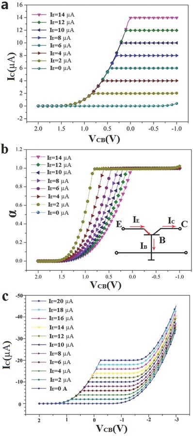
a) Measured forward common‐base output characteristics (I C ‐V CB) with a step size I E from 0 µA to 14 µA. b) The common‐base current gain (α) versus base–collector voltage (V CB) curves at room temperature. c). Base–collector junction is punctured through when further increasing V CB after saturation region.
It presents the efficiency of electrons from the emitter transferred to the collector in common‐base configure. The plot of the common‐base current gain (α) versus the base–collector voltage (V CB) displays a curve at room temperature and is shown in Figure 4b. α can reach 0.95, which means that I C is approximately equal to I E, with an extremely small difference at the saturation region. The ratio of holes, which are recombined by electrons in the base region, is small compared to all holes injected to the base from the emitter. The high‐efficiency of the current transmission is the best of any recently reported BJTs or hot electron transistors (HETs) based on 2D semiconductors.36, 37, 38, 39 In the active region, the emitter–base junction is forward‐biased, resulting in the lowering of the potential barrier and the narrowing of the space‐charge region (at the emitter–base junction) so that a significant number of holes can be injected from the emitter into the base region. The holes are gathered in the MoS2 layer and are rapidly diffused through the base terminal, thus I B is approximately equal to I E. With the further reduction of V CB, the base–collector junction is punctured and the I C increases rapidly, as shown in Figure 4c.
Different from the common‐base configuration, the emitter made the input and output common. The signal was applied between the base and the emitter, and the output was developed between the collector and emitter in the common‐emitter (CE) configuration, as shown in the inset of Figure 5 b. The output characteristic curves (Figure 5a) show the variation of the collector current, with a changing collector–emitter voltage V CE and a constant base current. In the active region, the curves exhibit an ascendant trend, where I C increases with V CE. In the saturation region, V CE became small and the collector–base junction was biased with a positive voltage, resulting in a sharp decrease of the I C. In this region, the collector current did not highly depend on the base current. However, the common‐emitter direct current gain of the BJT is defined as
| (3) |
Figure 5.
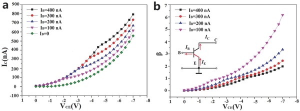
a) Measured forward common‐emitter output characteristics (I C ‐V CE) with a step size I B from 0 to 400 nA. b) The common‐emitter current gain (β) versus collector–emitter voltage (V CE) curves at room temperature.
Thus, β is the ratio of DC collector current to DC base current. The plot of the common‐emitter current gain (β) versus the emitter–collector voltage (V CE) curve at room temperature is shown in Figure 5b. The maximum β (≈7) can be achieved when V CE = −7 V and I B = 100 nA. The current gain of ≈7 is not the maximum value our device can achieve. As in the common‐emitter configuration, I C is not saturated, even when V CE was applied at −7 V. For the protection of our device, a higher voltage was not applied. Additionally, other NPN HBT‐based MoS2/GaTe/n‐Si heterostructures were also fabricated using the same methods provided in Section 4 of the Supporting Information, whose characteristics are not as good as ours but also shows conventional NPN BJT characteristics. Our device performance and properties are compared with other reported HBT/HET devices based on 2D materials and listed in Table 1 .36, 37, 38, 39, 40, 41 The theory of HETs is different than the theory of BJT/HETs, and there is a barrier between the emitter and the base layer in HETs. Nevertheless, the basic mechanism and performance index are similar. The performance of the current density, common‐emitter current gain, and current transmission coefficient is almost the best. This result suggests that our device is very competitive (in terms of performance) in the HBT/HET that is based on 2D materials.
Table 1.
Comparison of HBT/HET device performance and properties between this work and other reported devices based on 2D materials
To better interpret I–V characteristics of the HBT, band diagrams were obtained along the vertical dashed line and were used to reveal its working mechanism. This is show in Figure 2b. Based on the previous work,42, 43, 44 discussing the band diagrams of GaTe/MoS2 junctions, the band diagram of our device (without bias) is shown in Figure 6 a. In common‐base configurations (Figure 4a), V CB < 0 (V BC > 0, collector is biased with a positive voltage) and V BE > 0 (the emitter is biased with a positive voltage), which is the saturated state (band diagram as shown in Figure 6b). In this case, a reverse bias is applied on the base–collector junction. This results in the potential barrier increasing and the space‐charge region broadening at the base–emitter junction so that the holes can be injected from the base into the collector region. In the common‐emitter configuration (Figure 4c), if the V BE > 0 and V BC < 0, then the V CE >V BE > 0. In the amplification state, a forward bias is applied to the base–emitter junction (V BE > 0), resulting in the potential barrier lowering. The space‐charge region's narrowing at the base–emitter junction is made so that a significant number of holes can be injected from the emitter into the base region, as shown in Figure 6c. As the base–collector junction is reverse‐biased (V BC < 0), the holes diffusing to the edge of the depletion region of the base–collector junction are transferred to the collector immediately. A small number of holes are recombined by the electrons in the MoS2 flake for a few MoS2 layers. Therefore, the current input to the base is amplified, as are the common‐emitter output characteristics shown in Figure 5a,b, respectively. The difference between the saturation state and the amplification state is that the base–collector junction is biased by a positive voltage, hence the barrier potential is reduced and the space‐charge region at the junction also becomes narrow.
Figure 6.
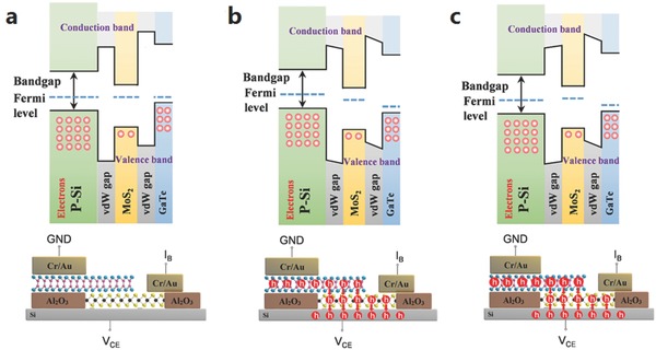
Band diagrams along the vertical dashed line in Figure 2b are shown in original state a), common‐base configuration (amplification state) b), common‐emitter configuration (saturation state) c), respectively.
In conclusion, we have successfully fabricated a bipolar junction transistor by combining GaTe, MoS2, and Si. Different from the BJT based on conventional bulk semiconductors, this device uses 2DLMs for the base and the emitter. This new BJT type has realized the typical characteristics of BJTs and the current amplification. Furthermore, the improved device performance can be achieved by optimizing the fabrication process. The 2D‐3D HBTs integrated with 2DLMs with conventional 3D bulk materials provide new exciting perspectives for the investigation of 2DLMs‐based amplifiers and integrated circuits.
Experimental Section
Device Fabrication and Electrical Characterization: This vertical HBT started with a commercially available Si‐wafer, slightly p‐doped with phosphorus. Before transferring MoS2, native oxide on the exposed Si substrate was carefully removed via the additional wet etching. Then, a few layers of MoS2 were exfoliated from the commercially available crystals on p‐type silicon substrates. After placing the MoS2 on the substrate, the wafer was annealed under vacuum (10−1 Pa) at 300 °C for 30 min, to remove any residue tapes. The insulating layer used for isolating the emitter and metal electrode from the collector was patterned using e‐beam lithography. Subsequently, without removing the photoresist, ≈40 nm of Al2O3 was deposited using the atomic layer deposition. Next, the photoresist was removed using acetone, after which only Al2O3 remained in the trenches and was washed away (with the resist) from the other regions. With the help of optical microscopy, the exfoliated GaTe was transferred directionally to the target MoS2 flake. Finally, electrode patterns were defined by a standard electron beam lithography (EBL) process and 10/60 nm Cr/Au electrodes were deposited via physical vapor deposition. Electrical properties of the fabricated devices were measured in a probe station using a semiconductor device parameter analyzer (Agilent, B1500A).
Conflict of Interest
The authors declare no conflict of interest.
Supporting information
Supplementary
Acknowledgements
X.Y. and D.W.Z. contributed equally to this work. This work was supported by National Natural Science Foundation of China (61622401, 61734003, 61376093, 21773036) and National Key Research and Development Program (2017YFB0405600, 2016YFA0203900).
Yan X., Zhang D. W., Liu C., Bao W., Wang S., Ding S., Zheng G., Zhou P., Adv. Sci. 2018, 5, 1700830 https://doi.org/10.1002/advs.542
References
- 1. Shockley W., Sparks M., Teal G., Phy. Rev. 1951, 83, 151. [Google Scholar]
- 2. Warnock J. D., IEEE Trans. Electron Devices 1995, 42, 377. [Google Scholar]
- 3. Kim K. H., Gaba S., Wheeler D., Cruzalbrecht J. M., Hussain T., Srinivasa N., Wei L., Nano Lett. 2012, 12, 389. [DOI] [PubMed] [Google Scholar]
- 4. Liu Y., Weiss N. O., Duan X., Cheng H.‐C., Huang Y., Duan X., Nat. Rev. Mater. 2016, 1, 16042. [Google Scholar]
- 5. Wang Q. H., Kalantar‐Zadeh K., Kis A., Coleman J. N., Strano M. S., Nat. Nanotechnol. 2012, 7, 699. [DOI] [PubMed] [Google Scholar]
- 6. Fiori G., Bonaccorso F., Iannaccone G., Palacios T., Neumaier D., Seabaugh A., Banerjee S. K., Colombo L., Nat. Nanotechnol. 2014, 9, 768. [DOI] [PubMed] [Google Scholar]
- 7. Chhowalla M., Jena D., Zhang H., Nat. Rev. Mater. 2016, 1, 16052. [Google Scholar]
- 8. Geim A. K., Novoselov K. S., Nat. Mater. 2007, 6, 183. [DOI] [PubMed] [Google Scholar]
- 9. Novoselov K. S., Geim A. K., Morozov S. V., Jiang D., Zhang Y., Dubonos S. V., Grigorieva I. V., Firsov A. A., Science 2004, 306, 666. [DOI] [PubMed] [Google Scholar]
- 10. Geim A. K., Science 2009, 324, 1530. [DOI] [PubMed] [Google Scholar]
- 11. Schwierz F., Nat. Nanotechnol. 2010, 5, 487. [DOI] [PubMed] [Google Scholar]
- 12. Lee J.‐H., Lee E. K., Joo W.‐J., Jang Y., Kim B.‐S., Lim J. Y., Choi S.‐H., Ahn S. J., Ahn J. R., Park M.‐H., Yang C.‐W., Choi B. L., Hwang S.‐W., Whang D., Science 2014, 344, 286. [DOI] [PubMed] [Google Scholar]
- 13. Bonaccorso F., Colombo L., Yu G., Stoller M., Tozzini V., Ferrari A. C., Ruoff R. S., Pellegrini V., Science 2015, 347, 1246501. [DOI] [PubMed] [Google Scholar]
- 14. Geim A. K., Grigorieva I. V., Nature 2013, 499, 419. [DOI] [PubMed] [Google Scholar]
- 15. Yu W. J., Li Z., Zhou H., Chen Y., Wang Y., Huang Y., Duan X., Nat. Mater. 2013, 12, 246. [DOI] [PMC free article] [PubMed] [Google Scholar]
- 16. Tosun M., Chuang S., Fang H., Sachid A. B., Hettick M., Lin Y., Zeng Y., Javey A., ACS Nano 2014, 8, 4948. [DOI] [PubMed] [Google Scholar]
- 17. Sachid A. B., Tosun M., Desai S. B., Hsu C. Y., Lien D. H., Madhvapathy S. R., Chen Y. Z., Hettick M., Kang J. S., Zeng Y., Adv. Mater. 2016, 28, 2547. [DOI] [PubMed] [Google Scholar]
- 18. Yann‐Wen L., Torres J. C. M., Xiaodan Z., Hussam Q., R A. J., B L. M., Shin‐Hung T., Yumeng S., Lain‐Jong L., Wen‐Kuan Y., Sci. Rep. 2016, 6, 32503.27581550 [Google Scholar]
- 19. Lan Y. W., Torres C. M., Tsai S. H., Zhu X., Shi Y., Li M. Y., Li L. J., Yeh W. K., Wang K. L., Small 2016, 12, 5676. [DOI] [PubMed] [Google Scholar]
- 20. Cheng R., Jiang S., Chen Y., Liu Y., Weiss N., Cheng H. C., Wu H., Huang Y., Duan X., Nat. Commun. 2014, 5, 5143. [DOI] [PMC free article] [PubMed] [Google Scholar]
- 21. Cheng R., Bai J., Liao L., Zhou H., Chen Y., Liu L., Lin Y. C., Jiang S., Huang Y., Duan X., Proc. Natl. Acad. Sci. USA 2012, 109, 11588. [DOI] [PMC free article] [PubMed] [Google Scholar]
- 22.a) Agnihotri P., Dhakras P., Ji U. L., Nano Lett. 2016, 16, 4355; [DOI] [PubMed] [Google Scholar]; b) Duan X., Xu J., Wei Z., Ma J., Guo S., Liu H., Dou S., Small Methods 2017, 1, 1700156. [Google Scholar]
- 23. Zhang J., Jiang G., Goledzinowski M., Comeau F. J. E., Li K., Cumberland T., Lenos J., Xu P., Li M., Yu A., Small Methods 2017, 1, 1700237. [Google Scholar]
- 24. Zhu S., Gong L., Xie J., Gu Z., Zhao Y., Small Methods 2017, 1, 1700220. [Google Scholar]
- 25. Radisavljevic B., Radenovic A., Brivio J., Giacometti I. V., Kis A., Nat. Nanotechnol. 2011, 6, 147. [DOI] [PubMed] [Google Scholar]
- 26. Yu Z., Pan Y., Shen Y., Wang Z., Ong Z.‐Y., Xu T., Xin R., Pan L., Wang B., Sun L., Nat. Commun. 2014, 5, 5290. [DOI] [PubMed] [Google Scholar]
- 27. Qiu H., Xu T., Wang Z., Ren W., Nan H., Ni Z., Chen Q., Yuan S., Miao F., Song F., Song F., Long G., Shi Y., Sun L., Wang J., Wang X., Nat. Commun. 2013, 4, 2642. [DOI] [PubMed] [Google Scholar]
- 28. Qiu H., Pan L., Yao Z., Li J., Shi Y., Appl. Phys. Lett. 2012, 100, 123104. [Google Scholar]
- 29. Li S. L., Komatsu K., Nakaharai S., Lin Y. F., Yamamoto M., Duan X., Tsukagoshi K., ACS Nano 2014, 8, 12836. [DOI] [PubMed] [Google Scholar]
- 30. Agnihotri P., Dhakras P., Ji U. L., Nano Lett. 2016, 16, 4355. [DOI] [PubMed] [Google Scholar]
- 31. Qi C., Zhang C., Fei X., Yong Z., Wei L., Ye W., Tu W., Zou Z., Wang X., Min X., Sci. Rep. 2013, 3, 2315.23897010 [Google Scholar]
- 32. Steinhoff A., Kim J. H., Jahnke F., Rösner M., Kim D. S., Lee C., Han G. H., Jeong M. S., Wehling T. O., Gies C., Nano Lett. 2015, 15, 6841. [DOI] [PubMed] [Google Scholar]
- 33. Splendiani A., Sun L., Zhang Y., Li T., Kim J., Chim C., Galli G., Wang F., Nano Lett. 2010, 10, 1271. [DOI] [PubMed] [Google Scholar]
- 34. Choudhary N., Islam M. R., Kang N., Tetard L., Jung Y., Khondaker S. I., J. Phys.: Condens. Matter 2016, 28, 364002. [DOI] [PubMed] [Google Scholar]
- 35. Chowdhury R. K., Maiti R., Ghorai A., Midya A., Ray S. K., Nanoscale 2016, 8, 13429. [DOI] [PubMed] [Google Scholar]
- 36. C. T. Jr., Lan Y. W., Zeng C., Chen J. H., Kou X., Navabi A., Tang J., Montazeri M., Adleman J. R., Lerner M. B., Nano Lett. 2015, 15, 7905. [DOI] [PubMed] [Google Scholar]
- 37. Vaziri S., Lupina G., Henkel C., Smith A. D., Östling M., Dabrowski J., Lippert G., Mehr W., Lemme M. C., Nano Lett. 2013, 13, 1435. [DOI] [PubMed] [Google Scholar]
- 38. Zeng C., Song E. B., Wang M., Lee S., C. T. Jr., Tang J., Weiller B. H., Wang K. L., Nano Lett. 2013, 13, 2370. [DOI] [PubMed] [Google Scholar]
- 39. Vaziri S., Belete M., Dentoni L. E., Smith A. D., Lupina G., Lemme M. C., Östling M, Nanoscale 2015, 7, 13096. [DOI] [PubMed] [Google Scholar]
- 40. Zubair A., Nourbakhsh A., Hong J. Y., Meng Q., Yi S., Jena D., Jing K., Dresselhaus M., Palacios T., Nano Lett. 2017, 17, 3089. [DOI] [PubMed] [Google Scholar]
- 41. Lin C. Y., Zhu X., Tsai S. H., Tsai S. P., Lei S., Li M. Y., Shi Y., Li L. J., Huang S. J., Wu W. F., ACS Nano 2017, 11, 11015. [DOI] [PubMed] [Google Scholar]
- 42. Wang F., Wang Z., Xu K., Wang F., Wang Q., Huang Y., Yin L., He J., Nano Lett. 2015, 15, 7558. [DOI] [PubMed] [Google Scholar]
- 43. Yuan X., Tang L., Wang P., Chen Z., Zou Y., Su X., Zhang C., Liu Y., Wang W., Liu C., Nano Res. 2015, 8, 3332. [Google Scholar]
- 44. Yang S., Wang C., Ataca C., Li Y., Chen H., Cai H., Suslu A., Grossman J. C., Jiang C., Liu Q., ACS Appl. Mater. Interfaces 2016, 8, 2533. [DOI] [PubMed] [Google Scholar]
Associated Data
This section collects any data citations, data availability statements, or supplementary materials included in this article.
Supplementary Materials
Supplementary


