Background
Perovskite light-emitting diodes (PeLEDs) are fabricated with a structure of indium tin oxide (ITO)/poly(3,4-ethylenedioxythiophene):polystyrene sulfonate (PEDOT:PSS)/CH3NH3PbBr3 (MAPbBr3)/1,3,5-tris(2-N-phenylbenzimidazolyl) benzene (TPBi)/Ag. PEDOT:PSS films treated with alcohols including methanol, ethanol, and isopropanol are used to realize high-performance PeLEDs. Among them, by using PEDOT:PSS film treated by methanol as the hole transport layer, the PeLED with a maximum luminance of 2075 cd m−2 and a maximum current efficiency of 0.38 cd A−1 is achieved. Meanwhile, the result shows that the luminance of PeLEDs increases with the polarity of alcohol solvent. The conductivity of PEDOT:PSS films and crystallization of perovskite films are analyzed to gain a deep illumination into the influence of alcohol solvent treatment on device performance. It is also found that the treatment brings not only an improved hole injection capability but also a significantly enhanced crystallization of perovskite. This work indicates that our founding brings a simple and effective method to improve the device performance of PeLEDs.
Electronic supplementary material
The online version of this article (10.1186/s11671-018-2505-6) contains supplementary material, which is available to authorized users.
Keywords: Perovskite light-emitting diodes, PEDOT:PSS, Alcohol solvent treatment, Polarity, Luminance
Background
Organic-inorganic hybrid perovskite materials have attracted enormous research interest because of their excellent properties. These properties include low material cost, compatible with solution processing, superior carrier mobility, and tunable optical bandgap [1–5]. At the same time, perovskite materials have a narrow full width at half maximum (FWHM) and a high photoluminescence quantum yield (PLQY) [6–9]. These characters make perovskite materials become the promising candidates for information display and solid-state lighting source compared to organic light-emitting diodes [10, 11] and provide the premise for low-cost and roll-to-roll fabrication. In 2014, Friend and co-workers firstly reported a new perovskite light-emitting diode (PeLED) based on solution-processing organometal halide perovskite with a sandwich structure. In green PeLEDs, a maximum luminance of 364 cd m−2 and a maximum external quantum efficiency (EQE) of 0.1% were obtained [12]. Since then, many significant works have been carried out to study PeLEDs. In 2015, Tae-Woo Lee and co-workers boosted the current efficiency (CE) of PeLEDs to 42.9 cd A−1 by increasing the proportion of methylammonium bromide in perovskite precursor solution and using nanocrystalline pinning-process method in the process of spin-coating perovskite [13]. In 2016, Jianpu Wang and co-workers reported a PeLEDs based on self-organized multiple quantum wells, and they achieved a very high EQE up to 11.7% [14]. In 2017, Chih-Jen Shih and co-workers fabricated PeLEDs with a high PLQY up to 92% by adding low-dielectric-constant compound, poly(methyl methacrylate) (PMMA), into perovskite colloidal solution [15]. These previous works indicate that PeLEDs have a great development potential in high-performance aspect.
As well known, the frequently used device structure of PeLEDs is anode (on transparent substrate, i.e., light-output direction)/hole transport layer (HTL)/perovskite emission layer (EML)/electron transport layer (ETL)/cathode [16–19]. In this structure, poly(3,4-ethylenedioxythiophene):polystyrene sulfonate (PEDOT:PSS) is the most common hole transport material because of its high transparency in the visible range (380–760 nm) and compatible with solution processing [20, 21]. However, the hole injection capability from PEDOT:PSS layer to EML is low. The main reason for this is that there is a high hole injection barrier from pristine PEDOT:PSS layer to EML, which caused by the highest occupied molecular orbital (HOMO) of PEDOT:PSS layer (5.2 eV) is much shallower than the HOMO of perovskite layer (5.6–5.9 eV) [20–22]. This high hole injection barrier (0.4–0.7 eV) hinders hole injection into EML efficiently, thus leading to an imbalance of charge carriers in EML.
To alleviate this problem, lots of efforts have been made to reduce the hole injection barrier from PEDOT:PSS layer to EML. For example, Tae-Woo Lee and co-workers combined PEDOT:PSS with perfluorinated ionomer (PFI) as a self-organized buffer HTL [13, 23]. The HOMO of the buffer HTL (absolute value) increased gradually from the bottom surface (5.2 eV) to the top surface (5.95 eV). This gradual increase of HOMO level can facilitate hole injection into CH3NH3PbBr3 (MAPbBr3) more efficient than pristine PEDOT:PSS film. In green PeLEDs with a buffer HTL, a maximum luminance of 417 cd m−2 was achieved. Da Bin Kim and co-workers mixed PEDOT:PSS with MoO3 (PEDOT:MoO3) as a composite HTL to reduce the hole injection barrier [24]. When the amount of MoO3 powder in PEDOT:PSS dispersion solution is 0.7 wt%, the HOMO of PEDOT:MoO3 composite layer increased from 5.15 to 5.31 eV. But the addition of excessive MoO3 powder into PEDOT:PSS solution would decrease the efficiency of device, which is probably due to the non-uniform morphology of MAPbBr3 film caused by excessive MoO3. Although these methods can reduce hole injection barrier, they are all doping with new materials in PEDOT:PSS solution, which is not conductive to large-scale industrial fabrication. Therefore, there is an urgent requirement to develop a more convenient method.
In this work, a high-luminance PeLEDs with MAPbBr3 as the EML were fabricated by spin coating alcohol solvent on PEDOT:PSS films before annealing treatment. By analyzing the characteristics of methanol (MeOH), ethanol (EtOH), and isopropanol (IPA), it is found that the polarity of alcohol solvent is a dominant factor for the improvement of PeLEDs performance. Alcohols with high polarity can introduce a screening effect between positively charged PEDOT and negatively charged PSS, and so they can take away some insulator PSS from PEDOT:PSS during spin-coating process [20]. As a result, the hole injection capability from PEDOT:PSS to perovskite film is dramatically improved. Meanwhile, after treated by alcohols with high polarity, there is a smoother PEDOT:PSS film, which can help obtain smaller perovskite grains and better perovskite coverage by improving the surface energy of PEDOT:PSS film [25]. So MeOH with the highest polarity can greatly improve the maximum luminance of PeLEDs from 261 to 2075 cd m−2, and a maximum CE from 0.1 to 0.38 cd A−1.
Methods
Properties of alcohol solvent used in this paper are presented in Table 1. The device structure of PeLEDs and experimental operation process are shown in Fig. 1. Device structure was indium tin oxide (ITO)/PEDOT:PSS/MAPbBr3 (70 nm)/1,3,5-tris(2-N-phenylbenzimidazolyl) benzene (TPBi) (40 nm)/Ag (100 nm). In this device structure, ITO and Ag were used as the anode and cathode, respectively, while PEDOT:PSS, MAPbBr3, and TPBi were used as the HTL, EML, and ETL, respectively. ITO substrates with a sheet resistance of 15 Ω/sq. were consecutively cleaned with water-detergent solution, acetone solvent, deionized water, and IPA solvent in ultrasonic bath each for 15 min. After dried in an oven, these cleaned ITO substrates were treated with oxygen plasma for 15 min. Then, PEDOT:PSS was spin-coated at 5000 rpm for 60 s on ITO substrate. For control samples, PEDOT:PSS/ITO substrates were annealed at 120 °C for 20 min directly without any treatment. For experiment samples, MeOH, EtOH, and IPA were spin-coated on PEDOT:PSS/ITO substrates at 5000 rpm for 30 s, respectively; then, these substrates were annealed at 120 °C for 20 min. After that, all of these substrates were transferred into a nitrogen glove box. The MAPbBr3 solution in DMF (5 wt%) was spin-coated on PEDOT:PSS/ITO substrates with two steps (500 and 3000 rpm for 20 and 60 s, respectively). During the spin-coating process, 400-μL chlorobenzene (CB) was dropped onto these samples at countdown 40th second. Then, all of these samples were annealed at 100 °C for 10 min. TPBi about 40 nm was evaporated on top of perovskite film, followed by the deposition of Ag about 100 nm by thermal deposition in high vacuum condition. The overlap area between ITO anode and Ag cathode was 0.2 cm2, which was the active emission area of PeLEDs.
Table 1.
Physical properties of polar solvents used in this study [30]
| Chemical | Polarity (water = 100) | Dielectric constant (20 °C) | Solubility parameter (cal cm3)1/2 | Boiling point/°C (water = 100) |
|---|---|---|---|---|
| MeOH | 76.2 | 32.6 | 14.5 | 65 |
| EtOH | 65.4 | 22.4 | 13.4 | 78 |
| IPA | 54.6 | 18.3 | 11.5 | 82 |
Fig. 1.
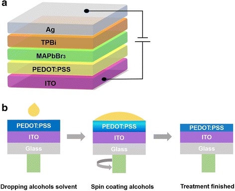
a Device structure of PeLEDs. b Process of spin coating alcohol solvent on PEDOT:PSS films
Device Characterization
The current density-voltage-luminance (J-V-L) characteristics were tested with a Keithley 4200 source. Electroluminescence (EL) spectra of PeLEDs were tested with a spectrophotometer OPT-2000. Device measurements were performed in air without encapsulation. Conductivity was measured by four-point probe technique with Hall Effect Measurement System (Suzhou Telecommunications Instrument Factory, SX 1934 (SZ-82)). Film thickness was measured by a step surface profiler. Surface morphologies of the PEDOT:PSS films and MAPbBr3 films were characterized by atomic force microscope (AFM; AFM 5500, Agilent, Tapping Mode, Chengdu, China). Crystallization of MAPbBr3 film was investigated by scanning electron microscopy (SEM; JEOL JSM-7100F). Crystal structure was characterized by X-ray diffraction (XRD; X’Pert PRO, PANalytical, Cu Kαradiation λ = 0.154056 nm, 40 kV, and 40 mA). The time-resolved photoluminescence (TRPL) spectra were recorded by a time-correlated single-photon counting system (FL-TCSPC, Horiba Jobin Yvon) with 368 nm picosecond (10−12 s) pulsed laser. The statistics of the obtained luminescent parameters for PeLEDs provided in Additional file 1: Figure S1 which are consistent with the Gaussian Distribution, showing that the results are statistically significant and reproducible, providing a strong proof of the discussion.
Results and Discussion
Performance of PeLEDs
Figure 2 shows the device performance with and without alcohols treating PEDOT:PSS films. And PeLED parameters, including maximum luminance (Lmax) and maximum CE (CEmax) are summarized in Table 2. The control devices without alcohol solvent treatment show a Lmax average of 261 cd m−2 and a CEmax average of 0.10 cd A−1. Compared to untreated devices, a higher Lmax average of 2075 cd m−2 is achieved for MeOH-treated devices with a CEmax average of 0.38 cd A−1. The EtOH-treated devices have a Lmax average of 1166 cd m−2 and CEmax average of 0.16 cd A−1, and the IPA-treated devices have a Lmax average of 863 cd m−2 and CEmax average of 0.22 cd A−1. Obviously, the Lmax of PeLEDs increase with the polarity of alcohol solvent increasing. We suspect that the improvement of device performance may be due to two reasons. One is that alcohol solvent treatment can facilitate the injection of hole into EML, and the other is that alcohol solvent treatment can promote the crystallization of MAPbBr3. As a result, the radiative recombination of excitons is enhanced. To verify the above postulation, the changes in PEDOT:PSS films and MAPbBr3 films are analyzed below.
Fig. 2.
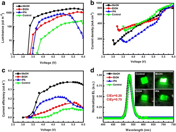
Device performance of PeLEDs. a Luminance-voltage (L-V) curves. b Current density-voltage (J-V) curves. c Current efficiency-voltage (CE-V) curves. d Normalized EL spectra and photographs of PeLEDs
Table 2.
Performance of PeLEDs based on treated PEDOT:PSS films
| HTL | Max. luminance (cd m−2 at bias) | Max. CE (cd A−1 at bias) |
|---|---|---|
| PEDOT:PSS | 261 (at 5.90 V) | 0.10 (at 5.90 V) |
| PEDOT:PSS-MeOH | 2075 (at 5.55 V) | 0.38 (at 5.55 V) |
| PEDOT:PSS-EtOH | 1166 (at 5.70 V) | 0.16 (at 5.70 V) |
| PEDOT:PSS-IPA | 863 (at 5.10 V) | 0.22 (at 5.10 V) |
We also examined the EL characteristics of PeLEDs. As shown in Fig. 2d, at the voltage of 5.5 V, the EL emission peaks of all devices center at 532 nm with a FWHM about 27 nm. Meanwhile, the luminescent photographs of PeLEDs were tested at 6.0 V. There are no additional emission peaks in the EL spectrum, indicating that the emission of these PeLEDs comes from MAPbBr3 merely.
Characterization of PEDOT:PSS Films
To illustrate the influence of alcohol solvent treatment on PEDOT:PSS films, the conductivity of PEDOT:PSS film is measured by a 4-point probe instrument. Conductivity values along with the pristine PEDOT:PSS films and after film treatment are shown in Table 3. As shown in Tables 1 and 3, the conductivity of PEDOT:PSS film increases with the enhancement of alcohol solvent polarity. Given this tendency, compared to 0.1 S cm−1 for pristine PEDOT:PSS film, the average conductivity values for PEDOT:PSS films treated with IPA and EtOH are 230.2 and 327.5 S cm−1, respectively. And for MeOH-treated films, an average conductivity of 605.0 S cm−1 can be achieved. It is well known that the Coulomb interaction between positively charged PEDOT and negatively charged PSS can be reduced by polar solvents [20]. Therefore, the alcohols with higher polarity is responsible for a stronger screening effect between PEDOT and PSS, so more amount of PSS are removed out with alcohols during the spin-coating process. As a result, the thickness of treated PEDOT:PSS film decreases, and the decline degree of film thickness varies with the polarity of alcohols solvent used. As shown in Table 3, the film thickness is 40 nm for untreated PEDOT:PSS layer, 27, 32, and 35 nm for MeOH-treated, EtOH-treated, and IPA-treated PEDOT:PSS films, respectively.
Table 3.
Properties of the treated PEDOT:PSS films
| HTL | Conductivity (S cm−1) | Thickness (nm) | RMS (nm) |
|---|---|---|---|
| PEDOT:PSS | 0.1 | 40 | 2.53 |
| PEDOT:PSS-MeOH | 605.0 | 27 | 0.90 |
| PEDOT:PSS-EtOH | 327.5 | 32 | 1.85 |
| PEDOT:PSS-IPA | 230.2 | 35 | 1.97 |
To further characterize the hole injection capability of PEDOT:PSS films after alcohol solvent treatment, the hole-only devices with a structure of ITO/PEDOT:PSS/MAPbBr3 (70 nm)/MoO3 (30 nm)/Ag (100 nm) are fabricated and measured the hole current density, which is shown in Fig. 3. It is obvious that MeOH-treated device has the highest current density than the control device, EtOH- and IPA-treated devices, presenting that the higher of the solvents’ polarity, the greater of hole injection capability from PEDOT:PSS layer to EML.
Fig. 3.
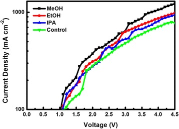
Current density versus voltage curves (CD-V) of hole-only PeLEDs with and without alcohol solvent treatments
The AFM measurement is conducted to investigate the morphology changes of PEDOT:PSS film surface. Figure 4 shows the topography images of pristine and treated PEDOT:PSS films on ITO substrates. The root mean square (RMS) roughness of film decrease from 2.53 nm for pristine PEDOT:PSS film to 0.90, 1.85, and 1.97 nm for MeOH-treated, EtOH-treated, and IPA-treated PEDOT:PSS films, respectively. It can be seen that the morphology of treated PEDOT:PSS film is more uniform than the pristine PEDOT:PSS, and MeOH-treated film has the best optimized uniform than EtOH- and IPA-treated films.
Fig. 4.
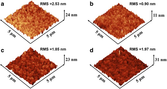
AFM morphology images of PEDOT:PSS films: a pristine PEDOT:PSS and b–d treated with MeOH, EtOH, and IPA, respectively
Characterization of MAPbBr3 Films
To investigate the effect of different alcohol treatment on MAPbBr3 film, the morphology and crystallization of MAPbBr3 are systematically studied. The AFM images of MAPbBr3 films based on PEDOT:PSS films treated with various alcohol solvent are shown in Fig. 5. For MAPbBr3 films based on pristine PEDOT:PSS films, the RMS roughness is 46.2 nm. And the RMS roughness of MAPbBr3 films decrease to 38.2, 38.7, and 39.5 nm for MeOH-treated, EtOH-treated, and IPA-treated PEDOT:PSS films, respectively. It can be seen that the decreased RMS roughness of MAPbBr3 films can smooth the MAPbBr3 films. And the RMS roughness of MAPbBr3 film decreases as the polarity of alcohol increases, which is consistent with the variation of PEDOT:PSS film’s RMS roughness.
Fig. 5.
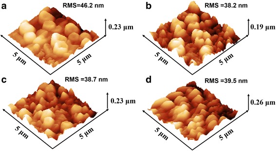
AFM morphology images of MAPbBr3 films: a based on pristine PEDOT:PSS film and b–d based on PEDOE:PSS films treated with MeOH, EtOH, and IPA, respectively
To further confirm the grain size and coverage of MAPbBr3 films, a top-view scanning electron microscopy (SEM) is used, and the micrograph is shown in Fig. 6. Obviously, MAPbBr3 film based on MeOH-treated PEDOT:PSS film has the smallest grain size and best coverage. The average grain size is estimated by Image J (an imaging processing software) using SEM micrographs. The average grain size of MAPbBr3 decrease from 328.0 nm for MAPbBr3 based on pristine PEDOT:PSS films to 232.0, 252.9, and 272.8 nm based on MeOH-treated, EtOH-treated, and IPA-treated PEDOT:PSS, respectively. And the MAPbBr3 coverage increase from 24.95 to 37.34% for MeOH-treated, 33.0% for EtOH-treated, and 28% for IPA-treated, respectively. Additionally, there are many small grains around the large grains in MeOH group and EtOH group, but few in IPA group and control group. The reason for this phenomenon may be that the growth of larger MAPbBr3 grains at the expense of smaller grains is prevented. And the reason for this retarding effect is that the surface energy of PEDOT:PSS film increases, where MAPbBr3 grains grow on. The more uniform the PEDOT:PSS film, the bigger the curvature, which is responsible for a larger surface energy [25]. It can be demonstrated that the introduction of alcohol solvent with high polarity will increase the surface energy of the PEDOT:PSS film by forming more uniform film, thereby reducing the possibility of small grains ablation or large grains grow bigger. This phenomenon is very consistent with crystal growth as Ostwald ripening and can be easily observed in the case of quantum dots materials [25, 26]. From the above analysis, we can see that the method of alcohol solvent treating PEDOT:PSS films does enhance the crystallization of MAPbBr3.
Fig. 6.
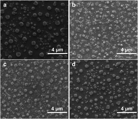
Top-view SEM images of MAPbBr3 films: a based on pristine PEDOT:PSS film and b–d based on PEDOT:PSS films treated with MeOH, EtOH, and IPA, respectively
The crystal structure of MAPbBr3 film is analyzed by measuring X-ray diffraction (XRD) patterns, as shown in Fig. 7a. The films have two strong and sharp diffraction peaks at 14.602o and 29.845o, corresponding to (100) and (200) planes, respectively. These two diffraction peaks are in good agreement with the previous report [27, 28], which demonstrates that MAPbBr3 crystals are highly oriented with a good cubic crystalline phase. To analyze the size of perovskite crystal, we can use Scherrer Equation as following:
| 1 |
where L (nm) represents the crystallite size, K (0.89, spherical) represents the Scherrer constant, λ (0.154056 nm) represents the X-ray wavelength, B (rad) represents full width at half maximum of the XRD peak, and θ (rad) represents X-ray angle. Using Eq. (1), we calculate the perovskite crystallite size to be 32.5 ± 0.8 nm. With the change of alcohol solvent, the variation of crystallite size is negligible. This proves that the crystal structure of MAPbBr3 does not change after alcohol solvent treatment. As shown in Fig. 7b, TRPL decay curves of MAPbBr3 films based on PEDOT:PSS films with and without MeOH treatments have been recorded. The PL decay curves are well described by bi-exponential decay function, which contains a slow decay and a fast decay. The fast decay is related to trap-assisted recombination (i.e., non-radiative recombination), and the lower decay is related to radiative recombination [3, 29]. When using MeOH to treat PEDOT:PSS films, the PL lifetime of excitons decreases, indicating that in the condition of unchanged composition and crystal structure of MAPbBr3, the efficiency of radiative recombination increases. From the above discussion, we see that alcohol solvent treatment on PEDOT:PSS films could manipulate the grain size and the coverage of perovskite films, which has a clear correlation between the morphology of PEDOT:PSS film and crystallization of perovskite.
Fig. 7.
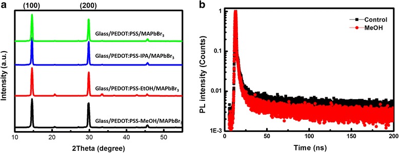
a XRD images of MAPbBr3 films and b time-resolved PL lifetime of MAPbBr3 films on PEDOT:PSS films with and without MeOH treatments
Conclusions
In conclusion, alcohol solvent treatment on PEDOT:PSS films has been proposed to improve the luminance of PeLEDs. Compared to EtOH and IPA, MeOH solvent is the most appropriate to improve PeLEDs performance, resulting in a Lmax of 2075 cd m−2 and a CEmax of 0.38 cd A−1. The luminance improvement can be attributed to the synergistic effect of alcohol solvent treatment. On the one hand, the higher the alcohol solvent polarity is, the more amount of PSS is taken away in the process of spin-coating alcohol solvent on PEDOT:PSS/ITO substrates. This will result in the higher conductivity of the treated PEDOT:PSS films, and more holes could be injected into perovskite active layer. On the other hand, the higher the alcohol polarity, the larger the surface energy of the PEDOT:PSS films, caused by their more uniform surface. The increased surface energy can restrain the Ostwald ripening and promote to grow smaller perovskite grains and better coverage, resulting in efficient radiative recombination. This provides that alcohol solvent treatment can be a valuable method to increase the baseline of PeLEDs performance, which will be widespread applicable in the future commercial production.
Additional File
Figure S1. Histogram of the maximum luminance of PeLEDs: (a) based on pristine PEDOT:PSS and (b–d) based on PEDOT:PSS films treated with MeOH, EtOH, and IPA, respectively. (DOCX 360 kb)
Acknowledgements
Not applicable
Funding
This work was financially supported by the Foundation of the National Natural Science Foundation of China (NSFC) (Grant Nos. 61675041 and 51703019), the Foundation for Innovation Research Groups of the NSFC (Grant No. 61421002), and the Science & Technology Department of Sichuan Province via Grant Nos. 2016HH0027 and 2016FZ0100.
Availability of Data and Materials
All data are fully available without restriction.
Abbreviations
- AFM
Atomic force microscope
- CB
Chlorobenzene
- CE
Current efficiency
- CEmax
Maximum current efficiency
- EL
Electroluminescence
- EML
Emission layer
- EQE
External quantum efficiency
- ETL
Electron transport layer
- EtOH
Ethanol
- FWHM
Full width at half maximum
- HOMO
The highest occupied molecular orbital
- HTL
Hole transport layer
- IPA
Isopropanol
- ITO
Indium tin oxide
- J-V-L
The current density-voltage-luminance
- Lmax
Maximum luminance
- MAPbBr3
CH3NH3PbBr3
- MeOH
Methanol
- PEDOT:MoO3
Mixed PEDOT:PSS with MoO3
- PEDOT:PSS
Poly(3,4-ethylenedioxythiophene):polystyrene sulfonate
- PeLEDs
Perovskite light-emitting diodes
- PFI
Perfluorinated ionomer
- PLQY
Photoluminescence quantum yield
- PMMA
Poly(methyl methacrylate)
- RMS
Root mean square
- SEM
Scanning electron microscopy
- TPBi
1,3,5-Tris(2-N-phenylbenzimidazolyl) benzene
- TRPL
The time-resolved photoluminescence
- XRD
X-ray diffraction
Authors’ Contributions
MW designed and carried out the experiments. MW, DZ, and ZW participated in the work to analyze the data and prepared the manuscript initially. JY gave materials and equipment supporting. All authors read and approved the final manuscript.
Authors’ Information
Mengge Wu received her B.A. degree from School of Optoelectronic Information at UESTC in 2016. She has been studying for her Master degree at State Key Laboratory of Electronic Thin Film & Integrated Devices (SKLETFID) & UESTC since 2016, where her main research interest is in PeLEDs.
Dan Zhao received his B.A. degree and Master degree from School of Material of Science and Engineering at Taiyuan University of Technology in 2013 and 2016, respectively. He has been studying for his Ph.D. degree at State Key Laboratory of Electronic Thin Film & Integrated Devices (SKLETFID) & UESTC since 2016. His main research interests are in interfacing engineering and photon management in organic semiconductor materials and devices.
Zijun Wang received his B.A. degree from School of Optoelectronic Information at UESTC in 2015. He has been studying for his Master degree at State Key Laboratory of Electronic Thin Film & Integrated Devices (SKLETFID) & UESTC since 2015, where his main research interests are in light-emitting diodes and photodetectors based on perovskite materials.
Junsheng Yu got his Ph.D. degree from Graduate School of Bio-Applications & System Engineering at Tokyo University of Agriculture and Technology in 2001. He is the Professor of SKLETFID & UESTC majoring in organic photoelectronic and electronic materials and devices.
Competing Interests
The authors declare that they have no competing interests.
Publisher’s Note
Springer Nature remains neutral with regard to jurisdictional claims in published maps and institutional affiliations.
Footnotes
Electronic supplementary material
The online version of this article (10.1186/s11671-018-2505-6) contains supplementary material, which is available to authorized users.
Contributor Information
Mengge Wu, Email: 947219216@qq.com.
Dan Zhao, Email: danzhao@std.uestc.edu.cn.
Zijun Wang, Email: 1938764831@qq.com.
Junsheng Yu, Email: jsyu@uestc.edu.cn.
References
- 1.Correa-Baena JP, Saliba M, Buonassisi M, Gratzel M, Abate A, Tress W, Hagfeldt A. Promises and challenges of perovskite solar cells. Science. 2017;358:739–744. doi: 10.1126/science.aam6323. [DOI] [PubMed] [Google Scholar]
- 2.Zhang LQ, Yang XL, Jiang Q, Wang PY, Yin ZG, Zhang XW, Tan HR, Yang Y, Wei MY, Sutherland BR, Sargent EH, You JB. Ultra-bright and highly efficient inorganic based perovskite light-emitting diodes. Nat Commun. 2017;8:15640. doi: 10.1038/ncomms15640. [DOI] [PMC free article] [PubMed] [Google Scholar]
- 3.Zhang XL, Liu H, Wang WG, Zhang JB, Xu B, Karen KL, Zheng YJ, Liu S, Chen SM, Wang K, Sun XW. Hybrid perovskite light-emitting diodes based on perovskite nanocrystals with organic-inorganic mixed cations. Adv Mater. 2017;29:1606405. doi: 10.1002/adma.201606405. [DOI] [PubMed] [Google Scholar]
- 4.Zheng YF, Shi W, Kong J, Huang D, Kartz HE, Yu JS, Taylor AD. A cytop insulating tunneling layer for efficient perovskite solar cells. Small Methods. 2017;1:1700244. doi: 10.1002/smtd.201700244. [DOI] [Google Scholar]
- 5.Li SB, Zhang P, Wang YF, Sarvari H, Liu DT, Wu J, Yang YJ, Wang ZM, Chen ZD. Interface engineering of high efficiency perovskite solar cells based on ZnO nanorods using atomic layer deposition. Nano Res. 2017;10:1092–1103. doi: 10.1007/s12274-016-1407-0. [DOI] [Google Scholar]
- 6.Kovalenko MV, Protesescu L, Bodnarchuk MI. Properties and potential optoelectronic applications of lead halide perovskite nanocrystals. Science. 2017;358:745–750. doi: 10.1126/science.aam7093. [DOI] [PubMed] [Google Scholar]
- 7.Kim YH, Cho H, Lee TW. Metal halide perovskite light emitters. Proc Natl Acsd Sci USA. 2016;113:11694–11702. doi: 10.1073/pnas.1607471113. [DOI] [PMC free article] [PubMed] [Google Scholar]
- 8.Li SB, Zhang P, Chen H, Wang YF, Liu DT, Wu J, Sarvari H, Chen ZD. Mesoporous PbI2 assisted growth of large perovskite grains for efficient perovskite solar cells based on ZnO nanorods. J Power Sources. 2017;342:990–997. doi: 10.1016/j.jpowsour.2017.01.024. [DOI] [Google Scholar]
- 9.Veldhuis SA, Boix PP, Yantara N, Li MJ, Sum TC, Mathews N, Mhaisalkar SG. Perovskite materials for light-emitting diodes and lasers. Adv Mater. 2016;28:6804–6834. doi: 10.1002/adma.201600669. [DOI] [PubMed] [Google Scholar]
- 10.Zhao D, Qin ZN, Huang J, Yu JS. Progress on material, structure and function for tandem organic light-emitting diodes. Org Electron. 2017;51:220–242. doi: 10.1016/j.orgel.2017.09.023. [DOI] [Google Scholar]
- 11.Li J, Qi YG, Zhao D, Li M, Lu ZY, Yu JS. Pure white organic light-emitting devices with excellent color stability using a non-doped 4-aryloxy-1,8-naphthalimide derivative. J Lumin. 2017;192:463–469. doi: 10.1016/j.jlumin.2017.07.029. [DOI] [Google Scholar]
- 12.Tan ZK, Moghaddam RS, Lai ML, Docampo P, Higler R, Deschler F, Price M, Sadhanala A, Pazos LM, Credgington D, Hanusch F, Bein T, Snaith HJ, Friend RH. Bright light-emitting diodes based on organometal halide perovskite. Nat Nanotechnol. 2014;9:687–692. doi: 10.1038/nnano.2014.149. [DOI] [PubMed] [Google Scholar]
- 13.Cho HC, Jeong SH, Park MH, Kim YH, Wolf C, Lee CL, Heo JH, Sadhanala A, Myoung N, Yoo S, Im SH, Friend RH, Lee TW. Overcoming the electroluminescence efficiency limitations of perovskite light-emitting diodes. Science. 2015;350:1222–1225. doi: 10.1126/science.aad1818. [DOI] [PubMed] [Google Scholar]
- 14.Wang NN, Cheng L, Ge R, Zhang ST, Miao YF, Zou W, Yi C, Sun Y, Cao Y, Yang R, Wei YQ, Guo Q, Ke Y, Yu MT, Jin YZ, Liu Y, Ding QQ, Di DW, Yang L, Xing GC, Tian H, Jin CH, Gao F, Friend RH, Wang JP, Huang W. Perovskite light-emitting diodes based on solution-processed self-organized multiple quantum wells. Nat Photonics. 2016;10:699–704. doi: 10.1038/nphoton.2016.185. [DOI] [Google Scholar]
- 15.Kumar S, Jagielski J, Kallikounis N, Kim YH, Wolf C, Jenny F, Tian T, Hofer CJ, Chiu YC, Stark WJ, Lee TW, Shih CJ. Ultrapure green light-emitting diodes using two-dimensional formamidinium perovskites: achieving recommendation 2020 color coordinates. Nano Lett. 2017;17:5277–5284. doi: 10.1021/acs.nanolett.7b01544. [DOI] [PubMed] [Google Scholar]
- 16.Kim SJ, Byun JW, Jeon TW, Jin HM, Hong HR, Kim SO. Perovskite light-emitting diodes via laser crystallization: systematic investigation on grain size effects for device performance. ACS Appl Mater Inter. 2018;10:2490–2495. doi: 10.1021/acsami.7b15470. [DOI] [PubMed] [Google Scholar]
- 17.Xiao ZG, Kerner RA, Zhao LF, Tran NL, Lee KM, Koh TW, Scholes GD, Rand BP. Efficient perovskite light-emitting diodes featuring nanometre-sized crystallites. Nat Photonics. 2017;11:108–115. doi: 10.1038/nphoton.2016.269. [DOI] [Google Scholar]
- 18.Wang ZJ, Li ZR, Zhou DL, Yu JS. Low turn-on voltage perovskite light-emitting diodes with methanol treated PEDOT:PSS as hole transport layer. Appl Phys Lett. 2017;111:233304. doi: 10.1063/1.5010245. [DOI] [Google Scholar]
- 19.Sun HZ, Yang ZY, Wei MY, Sun W, Li XY, Ye YS, Zhao YB, Tan HR, Kynaston EL, Schon TB, Yan H, Lu ZH, Ozin GA, Sargent EH, Seferos DS. Chemically addressable perovskite nanocrystals for light-emitting applications. Adv Mater. 2017;29:1701153. doi: 10.1002/adma.201701153. [DOI] [PubMed] [Google Scholar]
- 20.Alemu D, Wei HY, Ho KC, Chu CW. Highly conductive PEDOT:PSS electrode by simple film treatment with methanol for ITO-free polymer solar cells. Energy Environ Sci. 2012;5:9662–9671. doi: 10.1039/c2ee22595f. [DOI] [Google Scholar]
- 21.Li QD, Yang JW, Chen SS, Zou JZ, Xie WG, Zeng XR. Highly conductive PEDOT:PSS transparent hole transporting layer with solvent treatment for high performance silicon/organic hybrid solar cell. Nanoscale Res Lett. 2017;12:506. doi: 10.1186/s11671-017-2276-5. [DOI] [PMC free article] [PubMed] [Google Scholar]
- 22.Zheng D, Yang GJ, Zheng YF, Fan P, Ji R, Huang J, Zhang WK, Yu JS. Carbon nano-onions as a functional dopant to modify hole transporting layers for improving stability and performance of planar perovskite solar cells. Electrochim Acta. 2017;247:548–557. doi: 10.1016/j.electacta.2017.07.061. [DOI] [Google Scholar]
- 23.Cho H, Wolf C, Kim JS, Yun HJ, Bae JS, Kim H, Heo JM, Ahn S, Lee TW. High-efficiency solution-processed inorganic metal halide perovskite light-emitting diodes. Adv Mater. 2017;29:1700579. doi: 10.1002/adma.201700579. [DOI] [PubMed] [Google Scholar]
- 24.Kim DB, Yu JC, Nam YS, Kim DW, Jung ED, Lee SY, Lee S, Park JH, Lee AY, Lee BR, Di Nuzzo D, Friend RH, Song MH. Improved performance of perovskite light-emitting diodes using a PEDOT:PSS and MoO3 composite layer. J Mater Chem C. 2016;4:8161–8165. doi: 10.1039/C6TC02099B. [DOI] [Google Scholar]
- 25.Mohammadi P, Sharma P. Atomistic elucidation of the effect of surface roughness on curvature-dependent surface energy, surface stress, and elasticity. Appl Phys Lett. 2012;100:133110. doi: 10.1063/1.3695069. [DOI] [Google Scholar]
- 26.Chan WCW, Maxwell DJ, Gao XH, Bailey RE, Han MY, Nie SM. Luminescent quantum dots for multiplexed biological detection and imaging. Curr Opin Biotech. 2002;13:40–46. doi: 10.1016/S0958-1669(02)00282-3. [DOI] [PubMed] [Google Scholar]
- 27.Yu JC, Kim DB, Jung ED, Lee BR, Song MH. High-performance perovskite light-emitting diodes via morphological control of perovskite films. Nano. 2016;8:7036–7042. doi: 10.1039/c5nr05604g. [DOI] [PubMed] [Google Scholar]
- 28.Luo W, Wu CC, Sun WH, Guo X, Xiao LX, Chen ZJ. High crystallization of perovskite film by a fast electric current annealing process. ACS Appl Mater Inter. 2017;9:26915–26920. doi: 10.1021/acsami.7b07775. [DOI] [PubMed] [Google Scholar]
- 29.Jiao B, Zhu XB, Wu W, Dong H, Xia B, Xi J, Lei T, Hou X, Wu ZX. A facile one-step solution deposition via non-solvent/solvent mixture for efficient organometal halide perovskite light-emitting diodes. Nano. 2016;8:11084–11090. doi: 10.1039/c6nr01092j. [DOI] [PubMed] [Google Scholar]
- 30.Smallwood IM. Handbook of organic solvent properties. Sydney: Halsted Press; 1996. [Google Scholar]
Associated Data
This section collects any data citations, data availability statements, or supplementary materials included in this article.
Supplementary Materials
Figure S1. Histogram of the maximum luminance of PeLEDs: (a) based on pristine PEDOT:PSS and (b–d) based on PEDOT:PSS films treated with MeOH, EtOH, and IPA, respectively. (DOCX 360 kb)
Data Availability Statement
All data are fully available without restriction.


