Abstract
We introduce a hybrid CMOS-graphene sensor array for sub-second measurement of dopamine via fast-scan cyclic voltammetry (FSCV). The prototype chip has four independent CMOS readout channels, fabricated in a 65 nm process. Using planar multilayer graphene as biologically compatible sensing material enables integration of miniaturized sensing electrodes directly above the readout channels. Taking advantage of the chemical specificity of FSCV, we introduce a region of interest technique, which subtracts a large portion of the background current using a programmable low-noise constant current at about the redox potentials. We demonstrate the utility of this feature for enhancing the sensitivity by measuring the sensor response to a known dopamine concentration in vitro at three different scan rates. This strategy further allows us to significantly reduce the dynamic range requirements of the analog-to-digital converter (ADC) without compromising the measurement accuracy. We show that an integrating dual-slope ADC is adequate for digitizing the background-subtracted current. The ADC operates at a sampling frequency of 5-10 kHz and has an effective resolution of about 60 pA, which corresponds to a theoretical dopamine detection limit of about 6 nM. Our hybrid sensing platform offers an effective solution for implementing next-generation FSCV devices that can enable precise recording of dopamine signaling in vivo on a large scale.
Keywords: Biosensor, Dual-slope ADC, Graphene, Dopamine, Electrochemical sensor, Cyclic voltammetry, FSCV
I. Introduction
THE brain is a chemically complex environment with many chemical messengers, including neurotransmitters and neuromodulators. Among those, dopamine is a crucial neuromodulator for action selection and reward-motivated behavior [1]–[3]. The role of dopamine in several pathological brain conditions, including drug addiction [4], schizophrenia [5], and Parkinsons disease [6] makes it crucial to devise efficient methods for its measurement in vivo. At present, repeated fast-scan cyclic voltammetry (FSCV) with carbon microfibers (CMFs) is the method of choice to measure transient dopamine release in the neural tissue. FSCV offers good chemical specificity and acceptable temporal resolution. Further, it has successfully been used for in vivo measurements in rodents [7], [8] and recently in humans and non-human primates [9]–[11]. However, two main challenges limit the utility of existing devices for large-scale measurement of dopamine neuromodulatory signals. First, the large size of cylindrical CMFs makes the miniaturization of the electrodes using standard microfabrication processes difficult, thereby limiting them to single-site measurements [12]. In fact, CMF electrodes are currently produced manually, resulting in significant variability of the device properties. Second, the signal of interest is small and thus susceptible to environmental noise. This is a limiting factor particularly in experiments involving large animals where the signal must travel a few centimeters along the probe inside the brain before it reaches the readout circuitry.
CMOS technology allows large-scale integration of silicon transistors, enabling compact systems with complex functionality. Leveraging this feature, a large body of work has demonstrated innovative CMOS chips for detecting various chemical analytes via cyclic voltammetry [13]–[18]. These integrated readout chips offer a number of remarkable advantages over the conventional readout methods, namely enhanced detection limit, massively parallel sensing, low power consumption, and a small footprint. Beyond cyclic voltammetry, a few studies have used CMOS chips to advance the FSCV readout systems, which are used for subsecond recording of neuromodulatory signals. These FSCV integrated circuits (ICs) are particularly useful to facilitate measurements in moving animals by making the readout unit compact, lighter, and possibly wireless [19]–[22].
The FSCV ICs are, in essence, analog-to-digital converters (ADC) that digitize the current signal produced during the FSCV measurements. Past design strategies of the FSCV ICs have aimed to cope with the large variations of the CMF electrodes. These variations originate from a number of factors including the structural inhomogeneity of CMF at the microscopic level and the inconsistency of the electrode size at the macroscopic level. Existing designs of the FSCV ICs use two strategies to accommodate this practical consideration. The first strategy has used oversampling ADCs with high resolution and high dynamic range (e.g. high-order ΣΔ modulators) for recording the total current [19]–[21]. A second strategy described in Ref. [22] has used an on-chip analog background current subtraction. This approach is conceptually similar to the original analog background subtraction technique, described in [23]. In this FSCV chip, the background current was first recorded using a Nyquist ADC at the beginning of each trial, prior to dopamine release, and subsequently stored into an on-chip memory unit. The saved background current was retrieved during dopamine measurements and subtracted in real time from the total current just before the conversion by the same ADC. These techniques have improved the quality of measurements. However, the variability of conventional probes and their fabrication process pose a fundamental challenge that cannot be easily surmounted by such approaches of the FSCV integrated circuits. This challenge is amplified by other considerations that one should take into account for improving the sensitivity of measurements. For example, it is often desired to boost the scan rates (up to 2000 V/s) [24] to lower the detection limit of CMF sensors, especially for in vivo studies. High scan rates amplify the background current to a few micro ampere (μA), requiring ADCs with both high accuracy and large dynamic range. These demands are often impossible to satisfy simultaneously with the needs to limit power consumption and circuit area, which are also required for most in vivo measurements.
To address the challenges imposed by the large variations of the traditional electrodes and the demand for large-scale recording of neuromodulators, we propose a hybrid CMOS-graphene sensor array, as shown in Fig. 1 [25]. To miniaturize the FSCV electrodes, we simply replace the conventional CMFs with planar multilayer graphene (MLG). The graphene electrodes are constructed directly above the CMOS chip because the electrode fabrication process is compatible with the CMOS post-processing steps. A main advantage is the precise control of the process to create homogeneous electrodes with reproducible properties, which contrasts with variability inherent to the manual manufacturing of CMF electrodes. Not only does the reproducible sensor properties relax the design requirements of FSCV ICs, but also it provides an opportunity to further simplify the design by leveraging the inherent FSCV characteristics. We do so by taking advantage of the chemical specificity of the FSCV output, in which the signal of interest (i.e. faradic current) occurs at about a given electrochemical potential. We refer to this potential range as the region of interest (ROI). Our CMOS chip subtracts a major portion of the background current in real time at the ROI using a programmable low-noise constant current source, while maintaining the shape of the signal. Our partial subtraction of the background current relaxes the conventional requirement for a high dynamic range ADC, without compromising the measurement accuracy or restricting the FSCV sensing parameters (i.e. electrode size and scan rate). Consequently, we can use a simple dual-slope integrating ADC to digitize the partially subtracted current.
Fig. 1.
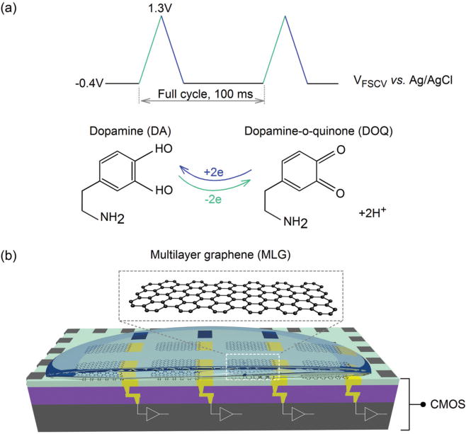
Schematic illustrations of (a) FSCV operating principle, and (b) our proposed hybrid graphene-CMOS sensor array.
A recent study by Kishida et al. suggests that the conventional analog background subtraction technique might produce unreliable measurements for low dopamine concentrations [11]. For example, they observed that this method confused changes in pH for changes in dopamine. By maintaining the shape of the signal at the ROI, our method gives an option for using newly developed algorithms in [11], [26] to reliably estimate low dopamine concentrations. This is particularly important to achieve high fidelity measurement of dopamine concentration. Finally, our sensor design allows us to place the readout chip in close physical vicinity to the sensor and further reduce detrimental effects of environmental noise, enhancing the limit of detection.
This paper is organized as follows. Section II explains practical considerations for the design of our FSCV IC. Section III describes our circuit design and system implementation. Section IV reports the results for the chip verification and in vitro dopamine tests.
II. Design considerations for FSCV IC
In this section, we first introduce the concept for region of interest, which we later use for implementing our current subtraction scheme. We then explain our strategy for applying the voltage waveform to the working electrode (WE). Finally, the electrical model of the MLG electrodes is provided for system simulations.
A. Region of interest in FSCV
FSCV is a variant of the electrochemical cyclic voltammetry that uses fast scan rates and high measurement frequency to achieve sub-second temporal resolution. FSCV has good specificity and thus highly useful for detecting target analytes in chemically complex environments. Because of its advantageous properties, FSCV is used extensively for recording transient dopamine release in the brain. Fig. 1a schematically illustrates the working principle of FSCV. A triangular voltage waveform is applied to the WE with a typical scan rate of 400 V/s and a repetition rate of 10 Hz. In one full cycle, the voltage is varied relative to a Ag/AgCl reference electrode (RE) between −0.4 V to 1.3 V and back to −0.4 V and is then held at this potential until the start of the next cycle. The dopamine molecules undergo a redox reaction as a result of the voltage ramp applied to the WE, as shown in Fig. 1a. Specifically, dopamine is oxidized during the voltage ramp-up, producing dopamine-o-quinone (DOQ) and two free electrons. This charge transfer process produces a faradic current (IDA) with a positive polarity, indicating the flow of the current into the WE, as shown in Fig. 2d. Importantly, the amplitude of this faradic current is proportional to the dopamine concentration. DOQ is subsequently reduced back to dopamine during the voltage ramp-down, producing a faradic current with a negative polarity, i.e. the current flows out of the WE and into the readout circuitry.
Fig. 2.
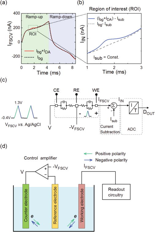
(a) Typical transient characteristics of the FSCV total current before (dashed) and after (solid) introducing dopamine, indicating the presence of a large background current. (b) Concept of region of interest (ROI), in which a large potion of the background current is removed at about the redox potentials using a constant current. (c) Architecture of our FSCV readout channel. (d) We use a three-electrode configuration for applying the FSCV voltage waveform to the WE.
When an ionic solution (an electrolyte) comes into contact with a non-faradic electrode, the re-arrangement of ions with opposing polarities on the surface of the electrode forms an interfacial electrical double layer. An apparent capacitance is associated with this layer, which is the fundamental property of the electrode-electrolyte interface. Therefore, applying a positive (negative) voltage ramp to the electrode will charge (discharge) the double-layer capacitance, producing a non- faradic current with positive (negative) polarity. The amplitude of this current is a function of te voltage scan rate and the double-layer capacitance. In FSCV, this current is known as the background current (Ibg) because it exists even in the absence of dopamine molecules in the electrolyte. Since the amplitude of the background current is independent of the dopamine concentration, and also that of other neuromodulators, we refer to it as the non-informative component of the total current. Once dopamine is introduced into the solution, the total current (IF SCV) includes both the background and the faradic currents. Fig. 2a shows the typical temporal responses of an MLG electrode to a dopamine-free phosphate-buffered saline (PBS) solution (dashed curve) and to a PBS solution with 1 μM dopamine (solid curve). We made these measurements using a discrete FSCV readout unit [27] that consists of a current pre-amplifier (SR570, Stanford Research Systems) and a data acquisition card (NI 6353 X series, National Instruments). From the data, it is evident that Ibg is significantly larger than the faradic current. The background current typically ranges from a few hundreds of nA to a few μA, depending on the scan rate and the size of the WE.
In FSCV, the oxidation (reduction) current peak for a given molecule occurs at specific positive (negative) electrochemical potentials. This specificity is highly useful for identifying a molecule in the presence of other chemicals. The precise control of the MLG electrode array fabrication allows us to take advantage of this fundamental property of FSCV to design a new current subtraction scheme. In our method, we first define the redox potential range as the region of interest, ROI. For example, the box region in Fig. 2a shows the ROI for the oxidation peak of dopamine. We then remove a large portion of Ibg in this region using a low-noise constant current (Isub), while maintaining the shape of the FSCV current at the ROI. Fig. 2b conceptually illustrates the current in the ROI after constant current subtraction. This current is then digitized using a high-resolution integrating ADC, as shown in Fig. 2c.
B. Applying voltage waveform to the working electrode
Previous FSCV ICs [19]–[22] adopted the conventional two-electrode configuration (WE and RE) for the voltammetry measurements. One practical concern in two-electrode measurements is the voltage drop across the RE, originating from the current flow through this electrode. The potential drop across the RE, therefore, introduces an error in determining the actual electrochemical potential that is applied to the WE. However, because of the small amplitude of the total current in FSCV (in low μA range or less), the potential drop across the RE is negligible. Therefore, the two-electrode configuration is adequate for FSCV measurements. Those ICs apply the voltage waveform using two strategies, depending on whether the readout scheme is continuous-time or discrete-time. In the continuous-time readout, the opamp in the first (gain or integrating) stage simultaneously functions as a potentiostat, where the waveform is simply applied to its non-inverting input terminal while the WE is connected to its inverting input terminal [19], [28]. On the other hand, the discrete-time readout requires a dedicated potentiostat in addition to the integration opamp. For example, a current-mirror-based potentiostat has been used in Ref [22], in which the waveform is applied to the non-inverting terminal of a unity-gain opamp while the WE is connected to the inverting input node. A 1:1 current mirror stage then transfers the FSCV current into the discrete-time Nyquist ADC. To eliminate the need for a current mirror and potential current scaling errors associated with the current mirror, we used a three-electrode configuration [29]. Fig. 2d schematically illustrates our approach. A voltage waveform (− VF SCV) is applied to the non-inverting terminal of a control amplifier. Due to the equivalent circuit of the electrodes in the solution (see Fig. 2c), the FSCV waveform then appears between the WE and RE.
C. Electrical model of MLG electrodes
To properly simulate the transient behavior of the electrodes in the solution and its effect on the stability of the system, it is necessary to develop a realistic electrical model for the electrodes. Fig. 3a illustrates the phenomenological small-signal electrical model of a non-faradic electrode. In this model, CEDL, RP, and RS are the double-layer capacitance, the parallel resistance at the electrode-electrolyte interface, and the solution resistance, respectively. To extract the values of the capacitance and the resistances, we first measured Ibg by applying the FSCV voltage waveform with a scan rate of 400 V/s to an MLG electrode in a PBS solution. Next, using a parametric sweep in Virtuoso (Cadence Virtuoso IC6.1.7), the model parameters were changed iteratively to match the simulated and measured transient currents. Fig. 3b shows the measured and simulated currents for a 1000 μm2 MLG electrode, giving the fitted model parameters of 1.1 nF, 500 MΩ, and 180 kΩ for CEDL, RP, and RS, respectively.
Fig. 3.
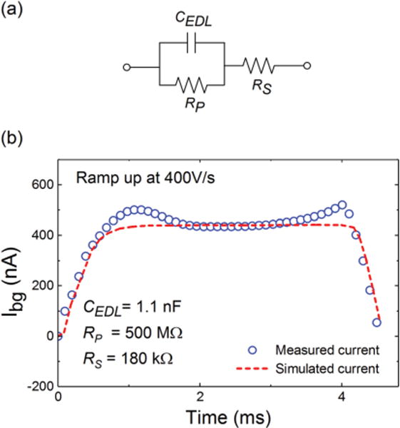
(a) Small-signal electrical model at the electrode-electrolyte interface. (b) We extracted the model parameters through simulations to match the simulated and the measured Ibg.
III. CMOS Circuit Implementation
This section focuses on the architecture of the readout channels and on the implementation of the circuit sub-blocks.
A. System architecture
Fig. 4 shows the architecture of our CMOS sensing platform comprising 4 independent channels. Each channel consists of the following circuit sub-blocks: a control amplifier to apply the FSCV waveform to the WE; a current subtraction unit to remove a large portion of the background current at the ROI; and a dual-slope ADC to digitize the background-subtracted current signal. The digital output of the dual-slope ADC is fed into digital buffers and driver circuits to improve the load driving capabilities. The FSCV voltage ramp is generated off-chip and is applied to the non-inverting node of the control amplifiers. A robust biasing circuit is implemented on-chip to provide the discharge current for the ADC, the low- noise constant current for the background subtraction block, and the biasing current for the operational amplifiers. The control digital block provides the control digital signals for operating the switches across the entire circuit. We use a two-stage operational transimpedance amplifier (OTA) as the control amplifier [30]. This OTA topology provides a large output voltage swing and sufficiently high slew rate, which are key design considerations for applying a large FSCV voltage waveform with a peak-to-peak amplitude of 1.7 V to the WE.
Fig. 4.
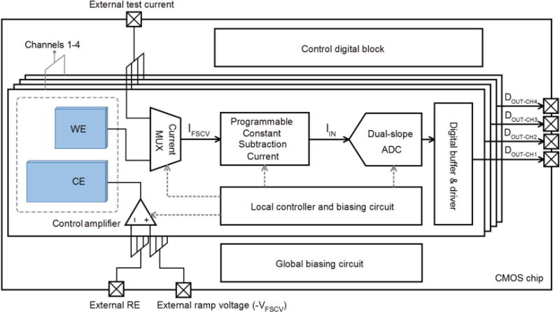
System architecture of our prototype readout circuit, consisting of 4 independent channels.
B. Current subtraction circuit
To relax the dynamic range requirement of the ADC, while maintaining the measurement accuracy, we implement a programmable current subtraction unit. This unit removes a large portion of Ibg before the signal is digitized by the ADC. The current subtraction unit has three key requirements. First, it should be low-noise with negligible DC offset error to avoid introducing unintentional noise or error to the FSCV signal. Second, it should be highly stable, particularly when the current subtraction branches are switched on or off. An improper design can lead to a range of issues from corrupting the signal of interest to making the entire system unstable. Finally, it should have a large dynamic range to make the sensing platform configurable for a wide range of FSCV experimental conditions including different electrode sizes and faster scan rates.
Fig. 5a schematically illustrates the current subtraction unit. This unit consists of a 5-bit digital-to-analog converter (DAC) and two robust low-noise current sources with opposing polarities. The combination of these sub-blocks makes this unit configurable, thus enabling a wide range of current subtractions up to 2.48 μA with a step of 80 nA for both positive and negative polarities. Fig. 5b shows a simplified schematic of the 5-bit current DAC. The biasing current and the biasing voltage VBP are supplied by the global current source unit, described later in section III-D. Depending on the polarity of the FSCV current signal, one of the switches, either Ssub,1 or Ssub,2, connects the proper current source to the input current path. The design of these switches needs special care because a poor design can corrupt the input signal or make the system unstable during the switching transience. Adjusting the impedance of the switches and matching them with that of the signal path is critical to avoid those problems. Specifically, when the switches are off, they must have sufficiently high impedance to fully disconnect the signal path from the current subtracting branch. On the other hand, it is desired that the switches have very small impedance in their on state. This will allow the current source branch to source (sink) a stable current to (from) the signal path when the polarity of the FSCV current is positive (negative). To meet the above requirements, we have chosen an optimal switch size of 4 μm/0.4 μm for the NMOS switch and 16 μm/0.4 μm for the PMOS switch from the transient simulations. Importantly, to compensate for the charge injection during transience, dummy switches are used. The lengths of the dummy and the main switches are identical, while the width of the main switches is two times larger than the width of the dummy switches.
Fig. 5.
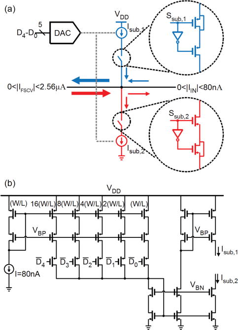
(a) Schematic illustration of the programmable current subtraction unit. (b) Schematic of the 5-bit current DAC, supplying a constant current up to 2.48 μA with a step of 80 nA.
C. Dual-slope integrating ADC
As discussed earlier in section II-A, the subtraction current unit removes a large portion of Ibg, significantly reducing the dynamic range requirement of the readout ADC. Another important specification of the ADC relates to its effective resolution. The physiological concentrations of dopamine in the brain can be as small as a few nM. Depending on the physical and geometrical properties of the electrode, such small concentrations translate into a faradic current in the range of hundreds of pA to a few nA. Resolving such a small current that is accompanied with the subtracted background current, therefore, requires an ADC with high accuracy. Additional ADC design considerations for this application include: (i) compact footprint to enable implementation of a dense sensor array, and (ii) low bit rate to facilitate data transmission and subsequent data analysis. We have chosen a dual-slope integrating ADC for digitizing the background-subtracted current because of its simplicity, high achievable accuracy, good linearity, and low bit rate. In our design, the ADC operates at a modest sampling frequency of 10 kHz during the in vitro measurements. Since for a nominal scan rate of 400 V/s the FSCV current signal occurs in a span of about 8.5 ms, this sampling rate is adequate to resolve the shape of the faradic current peak.
The ADC consists of a low-noise amplifier, a 2.5 pF MOM feedback capacitor, a latched comparator, and two discharge current sources with positive and negative polarities, as shown in Fig. 6a. The discharge current sources have the same amplitude of 10 nA. The design of the low-noise amplifier is based on the Recycling Folded Cascode (RFC) architecture [31], as shown in Fig. 6b. The RFC amplifier has a DC gain of 87 dB and consumes about 10 μA from a 1.8 V voltage supply. Fig. 6c shows the schematic of the latched comparator. To avoid false triggering of the comparator due to noise, the comparator has a Schmitt-trigger inverter at its output.
Fig. 6.
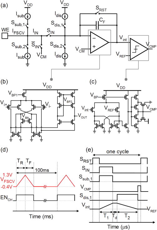
(a) Schematic of the readout circuit for measuring the FSCV current. (b) The integrator uses a low-noise RFC amplifier. (c) The latched comparator with a Schmitt-trigger inverter determines the full discharge of the capacitors. (d) Timing diagram of the FSCV voltage waveform. We enable the readout channels only during the voltage ramps. (e) Control and output signals of the dual-slope ADC.
Fig. 6d shows the timing diagram of the FSCV ramp signal VF SCV (top). Each channel has its own enable signal, ENCH. The ENCH and VFSCV signals are synchronized for the FSCV measurements. As a result, the dual-slope ADC only digitizes the current signal within this time period and is disabled during the rest period for energy saving. From the timing diagram, the duty cycle (α) of the circuit is 8.5% at 400 V/s. Considering the total power consumption of about 36 μW by the integrator and the comparator, we obtain an active power consumption of about 3.1 μW per channel.
The operating principle of a dual-slope ADC is simple. Fig. 6e shows the timing diagrams of the main signals within one cycle of the ADC operation. In this example, the Vint is the output of the integrator and corresponds to an input current signal with negative polarity, i.e. during the voltage ramp-down TF. After a short reset time SRST, the SIN switch is ON for a predefined time interval of T1 = 10 μs. During this time period, the ADC integrates the background-subtracted current signal IIN. After a short delay, the stored charge across the capacitor CF is gradually removed using a known discharge current Idis with an opposing polarity to that of IIN, i.e. Idis,2 in this example. Once the capacitor is fully discharged, the output voltage of the integrator reaches the common-mode again, which is equal to the VREF of the comparator. At this time, the comparator output switches from low to high, triggering the control circuit to stop the discharge period, Sdis,1. The background-subtracted current IIN is then simply calculated from the measured discharge time of T2 using:
| (1) |
In our design, we set the maximum values of T2 at sampling frequencies of 5 kHz and 10 kHz to 180 μs and 80 μs, respectively. Considering T1 = 10 μs and Idis = 10 nA, these maximum discharge times correspond to nominal IIN,max of 180 nA and 80 nA at 5 kHz and 10 kHz, respectively. Therefore, given the maximum Isub of 2.48 μA, our readout system can accommodate an input current up to 2.56 μA at 10 kHz sampling frequency.
D. Current source circuit
From equation 1, it is clear that a time-dependent error in the discharge current will directly compromise the accuracy of the ADC. Therefore, the discharge currents must be robust to time-dependent sources of error (e.g., environmental noise). To achieve this goal, we split the current source circuit into two sub-circuits: a global current source and a local current source. Fig. 7a shows the transistor-level schematic of the current source circuit. The global current source is common among the four measuring channels. It uses an external 10 μA current to generate the biasing voltages and the biasing current for the current subtraction unit, discussed in section III-B. In contrast, the local current source is implemented inside each channel. The branch consisting of the M23, M24, and M25 transistors locally regenerates the biasing voltage VBN from the global voltage VBP at node ”X” (see Fig. 7a). Three 10:1 down-conversion steps then generates the reference current. Regenerating this biasing voltage inside each local current source provides two key benefits. First, it diminishes the sensitivity of the local current source to possible small signal variations of the global biasing voltage VBP. Second, it improves the performance of the local current source against process variations, as shown in Fig. 7b.
Fig. 7.
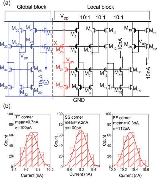
(a) Schematic illustration of the current source with global and local circuit sub-blocks. The global circuit is shared among all channels while each channel has its own local sub-block for generating the reference current. (b) Implementing the local circuit sub-blocks is important for making the design robust to process variations.
IV. Experimental results
A. Chip fabrication
We fabricated the circuit in a standard 65 nm CMOS process. The prototype chip consists of four readout channels. Post-processing was done to fabricate graphene microelectrodes on top of the chip. Owing to its planar structure, multilayer graphene is compatible with nano-fabrication processes. The illustration in Fig. 8a shows the cross-section view of the key fabrication processing steps. The post-processing starts with the transfer of a commercial MLG film (Graphene Supermarket) onto the CMOS chip. The MLG films are grown on nickel foils. For the transfer process, the nickel foil is fully removed in ferric chloride [32], followed by transfer of the free-standing MLG film onto the surface of the CMOS chip. The graphene electrodes are subsequently defined through a series of lithographic and metal deposition steps. A final electron beam lithographic step using an SU8 resist defines the sensing region of the MLG electrodes (1000 μm2) and further protects the metal electrodes from exposing to the solution. Fig. 8b shows the micrograph of the CMOS-graphene prototype chip. The scanning electron microscopy (SEM) image in Fig. 8c shows the close-up view of the MLG sensor array. The nano-fabrication processes allows us to create homogeneous MLG sensors with reproducible properties. This feature is key for implementing our proposed ROI concept. As a consequence, we achieve a channel size of 150 μm × 500 μm, which is adequately small for realizing a dense array of FSCV sensors. Figure 8d illustrates the layout of our FSCV readout channel. After post-processing, the chip is wire-bonded to a carrier board. Finally, a chemical-resist epoxy is used to protect the bonding wires and the metal pads only at the peripheral regions of the chip, while leaving the chip surface exposed for chemical sensing.
Fig. 8.
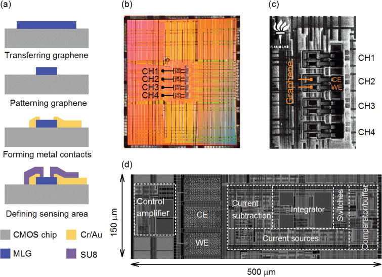
(a) Schematic illustration of the key post-processing steps for constructing the MLG sensor array above the CMOS chip. (b) Micrograph of the CMOS-graphene prototype chip. (c) Top-view SEM image of the post-processed chip, illustrating the MLG sensor array. (d) The illustration of the circuit layout of a readout channel. The size of the CMOS channel is 150 μm× 500 μm.
B. Chip verification
To verify the functionality of the circuit, we developed a test measurement setup, shown in Fig. 9. The main components of the test setup are: (i) a main printed circuit board that hosts external buffers, biasing circuits, and an FPGA interface circuit, (ii) a carrier board that hosts the fully-processed chip, (iii) an FPGA board (Xilinx Spartan 3E) that provides control signals and performs data acquisition, and (iv) injection pumps that supply solutions for in vitro experiments.
Fig. 9.
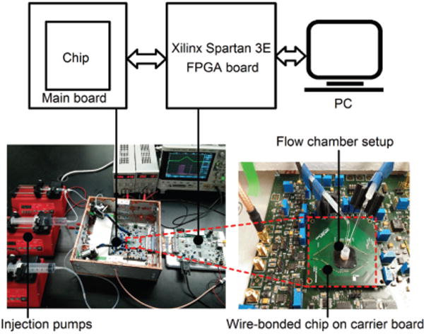
Photograph of the measurement setup. Injection pumps sequentially introduce PBS and dopamine solutions into the flow chamber. The FPGA records the digitized data from the readout channels.
To perform electrical characterization of the chip, we used a built-in test circuit. For the chip verification experiments in this paper, we operated the ADC at a sampling frequency of 5 kHz. We first examined the linearity of the circuit by injecting known constant currents into the ADC and recording the discharge time T2, which we then used to calculate the current using equation 1. Fig. 10a shows the plot for the measured current as a function of the injected test current, confirming linear behavior of the ADC up to 165 nA. We evaluated the signal-to-noise ratio (SNR) of the ADC using 100 Hz sinusoidal input currents with varying amplitudes in the range of 1-175 nA. We were unable to measure the SNR below 1 nA because of difficulties to generate sinusoidal waveforms with such small amplitudes. The inset in Fig. 10b shows a representative measured sinusoidal current waveform with an amplitude of 165 nA at the output of the ADC. The corresponding power spectral density (PSD) of the measured waveform is shown in Fig. 10b. From these measurements, we then computed the SNR of the ADC, shown in Fig. 10c. The ADC achieves a maximum SNR of 70.7 dB at 165 nA. The data in Fig. 10b also suggests a maximum signal-to-noise-distortion ratio (SNDR) of 62.4 dB, corresponding to 10 effective number of bits (ENOB). The ENOB extracted from the maximum SNDR is limited by the non-linearity of the test circuit. The simulation results indicate an ENOB of 11.6. The fit to the measured SNR data indicates a quantization-noise- free detection limit of about 30 pA. To verify this, we used the expression for the quantization-noise-free SNR of the ADC, which is given by [29]:
| (2) |
where is the mean square voltage at the integrator output and is given by . The other terms in the denominator of equation 2 represent the mean square voltage of the different sources of noise, which are: thermal noise of the WE , thermal noise of the discharge current source , integrated kT/CF noise during the reset period , and the OTA noise . This SNR expression assumes that these different sources of noise are uncorrelated. We found the root mean square of these sources of noise, summarized in Table I, either using the analytical models in [29] or using circuit simulations. Assuming SNR = 1, we obtain a quantization- noise-free of about 19 pArms. This value represents the input-referred noise and is consistent with the data in Fig. 10c.
Fig. 10.
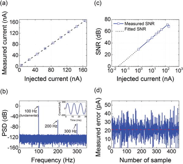
(a) Linear behavior of the ADC verified by injecting known DC currents. (b) Power spectral density of the ADC output corresponding to a sinusoidal input current of 165 nA. The inset shows the reconstructed signal at the ADC output. (c) SNR of the readout channel, measured by applying sinusoidal current signals with varying amplitudes at the input, indicating a maximum SNR of 70.7 dB. (d) We measured the ADC error by applying a slow current ramp rising at 10 nA/s and then subtracting each two consecutive measurements. The error (σ) is about 20 pArms, corresponding to an accuracy of 60 pA (3σ).
TABLE I.
Summary of different noise sources.
| Noise source | Value | |
|---|---|---|
|
|
5.1 μVrms | |
|
|
14.5 μVrms | |
|
|
40.5 μVrms | |
|
|
15.6 μVrms | |
| Total | 75.7 μVrms |
In our design, a small residual background current will always accompany the faradic current. Specifically, the constant subtraction current during the FSCV measurements is set such that the residual background current is in the range of several nA, which is adequately larger than the minimum detectable current by the ADC. Therefore, the minimum detectable current is not a limiting factor for accurate measurement of the dopamine concentration in our FSCV experiments. Rather, the measurement resolution of the ADC is the key parameter for this application. To experimentally verify the effective resolution of the ADC, we measured the ADC error by applying a very slow ramp current starting at 40 nA and increasing at a rate of 10 nA/s. This ramp rate corresponds to a current change of about 2 pA in each measuring cycle of the ADC (considering 5 kHz sampling frequency), which is much smaller than the expected ADC error. Therefore, subtracting each measured current from its immediate previous neighbor provides a good estimate of the ADC error. Fig. 10d shows the measured ADC error, indicating an error of about 20 pArms, which is consistent with the calculated input referred noise. Assuming an SNR of 3, the measured error corresponds to an effective resolution of 60 pA.
C. In vitro measurements
We now proceed to describe the performance of the chip using in vitro measurements. For the in vitro measurements, we operated the ADC at a sampling frequency of 10 kHz. Based on our experience, this sampling frequency is adequate for resolving the oxidation peak even at fast scan rates because the time-dependent full-width half-max of the FSCV peak is largely invariant to the scan rate. A 10 kHz operating frequency in our design corresponds to a maximum IIN of 80 nA.
While the operating principle of our readout chip is based on partial subtraction of the background current at the ROI, the sensing platform is capable of fully constructing Ibg by piecewise measurement of the current in a few FSCV cycles. To do so, our DAC code utilizes a stepwise increase of the subtraction current while the ADC records the corresponding current-subtracted Ibg. The subtraction current is initially zero in the first cycle but gradually increases in steps of 80 nA in subsequent cycles. The measurement continues for a number of FSCV cycles (e.g. 8 cycles for Ibg of 500 nA) until the current measured by the ADC is zero during the entire FSCV cycle. This condition indicates that the subtraction current has exceeded the maximum amplitude of Ibg, which we use to signal the end of the measurement for reconstruction of background current. Because the time stamps of the ADC output bits are known in FSCV and the background current is stable, the sum of the measured currents at each time stamp gives the background current at that time. The constructed Ibg(t) is thus given by:
| (3) |
where Ts is the time period of the FSCV cycle (100 ms in our experiments) and m is the FSCV cycle at which Isub exceeds maximum Ibg. Fig. 11a illustrates the constructed Ibg for three different scan rates. As discussed in section II-A, it is desired to increase the amplitude of the faradic signal using either larger electrodes or faster scan rates. However, these trends simultaneously increase Ibg, as shown in Fig. 11a. To evaluate the utility of our proposed ROI scheme, we measured the response of the hybrid sensing platform to a dopamine solution in PBS at these scan rates. In our experiments, we sequentially introduced a PBS solution and a dopamine solution in PBS into the flow chamber using injection pumps. To determine the subtraction current at the ROI, we used the constructed Ibg curves in Fig. 11a. Fig. 11b shows the measured IIN by the ADC before and after introducing a 2 μM dopamine solution into the flow chamber. Taking the difference of the IIN data between these two measurements gives the faradic signal due to the dopamine solution (dashed red curves). The solid grey bands in each panel represent the ROI. For in vivo measurements, it is critical to distinguish different neurotransmitters using their corresponding oxidation potentials in the FSCV voltammogram. This requires the simultaneous recording of their oxidation peaks. However, the relatively narrow ROI in Fig. 11b reveals the limitation of our current design for capturing the oxidation peaks that might occur outside the ROI. The limited width of the ROI in our design originates from the identical measuring range of the ADC and the Isub step (both 80 nA). This problem can be easily mitigated in our future work by designing a programmable Isub that allows current subtraction at smaller steps.
Fig. 11.
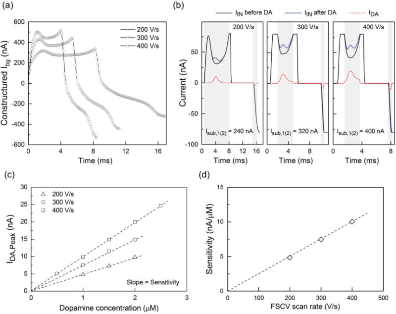
(a) Ibg can be fully constructed by the piecewise measurement of IIN while sweeping the DAC code. The data indicates the increase of Ibg with increasing the scan rate. (b) In vitro measurements of 2 μM dopamine at three different ramp rates. The grey regions represent the ROI. The results confirm our design is configurable in that it allows the user to increase the sensitivity with increasing the scan rate without being limited by the ADC full-range. (c) Calibration plots for three different scan rates. The slope of the linear fit represents the electrode sensitivity. (d) The plot of electrode sensitivity as a function of the scan rate, where the linear fit to the data suggests an adsorption-limited reaction.
Before performing in vivo experiments, it is important to obtain a calibration plot that represents the sensor response as a function of known dopamine concentrations. For in vivo measurements, this plot serves as a reference for estimating the unknown concentration of dopamine from the measured output of the sensor. Fig. 11c illustrates the representative calibration curves obtained at the scan rates of 200-400 V/s. The slope of a linear fit to the data is referred to as electrode sensitivity. The summary of the extracted sensitivity for different scan rates is shown in Fig. 11d. The linear increase of sensitivity with increased scan rate indicates that the sensing measurements at these scan rates are adsorption limited, as observed previously [33]. These measurements confirm the effectiveness of our current subtraction scheme at the ROI, which allows us to increase the sensitivity to dopamine by adjusting the scan rate without being limited by limitations in the dynamic range of the ADC. The measured sensitivity of about 10 nA/μM at 400 V/s together with the ADC effective resolution of 60 pA gives a theoretical detection limit of about 6 nM for our hybrid sensing platform. Table II compares the performance of our sensing platform with the previous reports of FSCV ICs.
TABLE II.
Performance summary and comparison with the state-of-the-art.
| This work | JSSC’09 [20] | JSSC’14 [21] | TBioCAS’16 [22] | |
|---|---|---|---|---|
| Technology | 65 nm | 0.5 μm | 0.35 μm | 65 nm |
| Electrode material/type | Graphene/Integrated | CMF/Discrete | CMF/Discrete | CMF/Discrete |
| Channel size (μm2) | 150 × 500 | 180 × 1050 | 113 × 984 | N/A |
| Input current range | ± 2.56 μA | ± 430 nA | ± 950 nA | ± 430 nA |
| Dynamic current subtraction | Yes | No | No | Yes |
| RMS input-referred noise | 20 pA in ± 80 nA (1 kHz BW) (w/slow ramp at the input) |
57 pA in ± 750 nA (5 kHz BW) (w/open input) |
55 pA in ± 950 nA (5 kHz BW) (w/open input) |
92 pA in ± 430 nA (2 kHz BW) (w/open input) |
| Resolution | 60 pA | N/A | N/A | 50 pA |
| Power Supply (V) | 1.8 | 2.5 | -0.8, 1.7 | 1.2, 3.0 |
| Power consumption (μW) | 3.1 | 76 | 9.3 | 14.4 |
| Number of channels | 4 | 4 | 1 | 1 |
| Testing method | In vitro | In vivo | In vivo | In vitro |
V. Conclusion
The results presented here establish three key strategies for implementing our proposed hybrid CMOS-graphene sensing platform: (i) replacing traditional carbon fiber with multilayer graphene to integrate multiple miniaturized electrodes directly above the CMOS readout chip; (ii) introducing a region of interest technique to remove a large portion of the non- informative background current; and (iii) implementing a high- resolution dual-slope integrating ADC to accurately resolve the subtracted current signal. A combination of these features makes our hybrid sensing platform configurable, small, and power-efficient. Our design leads the way for implementing the next generation of FSCV devices that are capable of measuring dopamine concentration in multiple locations with high temporal resolution.
Acknowledgments
The authors acknowledge United Microelectronics Corporation (UMC) for the support and fabrication of the CMOS chip. This research used resources of the Center for Functional Nanomaterials, which is a U.S. DOE Office of Science Facility, at Brookhaven National Laboratory under Contract No. DE- SC0012704. DS acknowledges partial financial support by NSF-CMMI award 1728051. RK acknowledges partial financial support by NIMH grant R01MH109180-01.
Contributor Information
Bayan Nasri, Department of Electrical and Computer Engineering, Tandon School of Engineering, New York University, 6 MetroTech Center, Brooklyn, NY 11201 USA.
Ting Wu, Department of Electrical and Computer Engineering, Tandon School of Engineering, New York University, 6 MetroTech Center, Brooklyn, NY 11201 USA.
Abdullah Alharbi, Department of Electrical and Computer Engineering, Tandon School of Engineering, New York University, 6 MetroTech Center, Brooklyn, NY 11201 USA.
Kae-Dyi You, Department of Electrical and Computer Engineering, Tandon School of Engineering, New York University, 6 MetroTech Center, Brooklyn, NY 11201 USA.
Mayank Gupta, Department of Electrical and Computer Engineering, Tandon School of Engineering, New York University, 6 MetroTech Center, Brooklyn, NY 11201 USA.
Sunit P Sebastian, Department of Electrical and Computer Engineering, Tandon School of Engineering, New York University, 6 MetroTech Center, Brooklyn, NY 11201 USA.
Roozbeh Kiani, Center for Neural Science at New York University, 4 Washington Place, New York, NY 10003 USA.
Davood Shahrjerdi, Department of Electrical and Computer Engineering, Tandon School of Engineering, New York University, 6 MetroTech Center, Brooklyn, NY 11201 USA.
References
- 1.Glimcher PW. Understanding dopamine and reinforcement learning: The dopamine reward prediction error hypothesis. Proceedings of the National Academy of Sciences. 2011;108(Supplement 3):15 647–15 654. doi: 10.1073/pnas.1014269108. [DOI] [PMC free article] [PubMed] [Google Scholar]
- 2.Floresco SB. The nucleus accumbens: An interface between cognition, emotion, and action. Annual Review of Psychology. 2015;66(1):25–52. doi: 10.1146/annurev-psych-010213-115159. [DOI] [PubMed] [Google Scholar]
- 3.Costa RM. A selectionist account of de novo action learning. Current Opinion in Neurobiology. 2011;21(4):579–586. doi: 10.1016/j.conb.2011.05.004. [DOI] [PubMed] [Google Scholar]
- 4.Goldstein RZ, RZ G. Dysfunction of the prefrontal cortex in addiction: neuroimaging findings and clinical implications. Nature Reviews Neuroscience. 2011;12(11):652–669. doi: 10.1038/nrn3119. [DOI] [PMC free article] [PubMed] [Google Scholar]
- 5.Winterer G, Weinberger DR. Genes, dopamine and cortical signal-to-noise ratio in schizophrenia. Trends in Neurosciences. 2004;27(11):683–690. doi: 10.1016/j.tins.2004.08.002. [DOI] [PubMed] [Google Scholar]
- 6.Miller DB, OCallaghan JP. Biomarkers of parkinsons disease: Present and future. Metabolism - Clinical and Experimental. 2015;64(3):S40–S46. doi: 10.1016/j.metabol.2014.10.030. [DOI] [PMC free article] [PubMed] [Google Scholar]
- 7.Robinson DL, Venton BJ, Heien ML, Wightman RM. Detecting subsecond dopamine release with fast-scan cyclic voltammetry in vivo. Clinical Chemistry. 2003;49(10):1763–1773. doi: 10.1373/49.10.1763. [DOI] [PubMed] [Google Scholar]
- 8.Venton BJ, Wightman RM. Psychoanalytical electrochemistry: Dopamine and behavior. Analytical Chemistry. 2003;75(19):414 A–421 A. [Google Scholar]
- 9.Yoshimi K, Naya Y, Mitani N, Kato T, Inoue M, Natori S, Takahashi T, Weitemier A, Nishikawa N, McHugh T, Einaga Y, Kitazawa S. Phasic reward responses in the monkey striatum as detected by voltammetry with diamond microelectrodes. Neuroscience Research. 2011;71(1):49–62. doi: 10.1016/j.neures.2011.05.013. [DOI] [PubMed] [Google Scholar]
- 10.Schluter EW, Mitz AR, Cheer JF, Averbeck BB. Real-time dopamine measurement in awake monkeys. PLOS ONE. 2014;9(6):1–15. doi: 10.1371/journal.pone.0098692. [DOI] [PMC free article] [PubMed] [Google Scholar]
- 11.Kishida KT, Saez I, Lohrenz T, Witcher MR, Laxton AW, Tatter SB, White JP, Ellis TL, Phillips PE, Montague PR. Subsecond dopamine fluctuations in human striatum encode superposed error signals about actual and counterfactual reward. Proceedings of the National Academy of Sciences. 2016;113(1):200–205. doi: 10.1073/pnas.1513619112. [DOI] [PMC free article] [PubMed] [Google Scholar]
- 12.Cahill PS, Walker QD, Finnegan JM, Mickelson GE, Travis ER, Wightman RM. Microelectrodes for the measurement of catecholamines in biological systems. Analytical chemistry. 1996;68(18):3180–3186. doi: 10.1021/ac960347d. [DOI] [PubMed] [Google Scholar]
- 13.Mollazadeh M, Murari K, Cauwenberghs G, Thakor N. Wireless micropower instrumentation for multimodal acquisition of electrical and chemical neural activity. IEEE transactions on biomedical circuits and systems. 2009;3(6):388–397. doi: 10.1109/TBCAS.2009.2031877. [DOI] [PubMed] [Google Scholar]
- 14.Nazari MH, Mazhab-Jafari H, Leng L, Guenther A, Genov R. Cmos neurotransmitter microarray: 96-channel integrated potentiostat with on-die microsensors. IEEE transactions on biomedical circuits and systems. 2013;7(3):338–348. doi: 10.1109/TBCAS.2012.2203597. [DOI] [PubMed] [Google Scholar]
- 15.Guo J, Ng W, Yuan J, Li S, Chan M. A 200-channel area-power-efficient chemical and electrical dual-mode acquisition ic for the study of neurodegenerative diseases. IEEE transactions on biomedical circuits and systems. 2016;10(3):567–578. doi: 10.1109/TBCAS.2015.2468052. [DOI] [PubMed] [Google Scholar]
- 16.Agarwal A, Gural A, Monge M, Adalian D, Chen S, Scherer A, Emami A. A 4μw, adpll-based implantable amperometric biosensor in 65nm cmos. VLSI Circuits, 2017 Symposium on IEEE. 2017:C108–C109. [Google Scholar]
- 17.Jafari HM, Abdelhalim K, Soleymani L, Sargent EH, Kelley SO, Genov R. Nanostructured cmos wireless ultra-wideband label-free pcr-free dna analysis soc. IEEE Journal of Solid-State Circuits. 2014;49(5):1223–1241. [Google Scholar]
- 18.Nazari MH, Mujeeb-U-Rahman M, Scherer A. An implantable continuous glucose monitoring microsystem in 0.18 μm cmos. VLSI Circuits Digest of Technical Papers, 2014 Symposium on IEEE. 2014:1–2. [Google Scholar]
- 19.Roham M, Daberkow DP, Ramsson ES, Covey DP, Pakdeeronachit S, Garris PA, Mohseni P. A wireless ic for wide-range neurochemical monitoring using amperometry and fast-scan cyclic voltammetry. IEEE transactions on biomedical circuits and systems. 2008;2(1):3–9. doi: 10.1109/TBCAS.2008.918282. [DOI] [PubMed] [Google Scholar]
- 20.Roham M, Covey DP, Daberkow DP, Ramsson ES, Howard CD, Heidenreich BA, Garris PA, Mohseni P. A wireless ic for time-share chemical and electrical neural recording. IEEE Journal of Solid-State Circuits. 2009;44(12):3645–3658. [Google Scholar]
- 21.Bozorgzadeh B, Covey DP, Howard CD, Garris PA, Mohseni P. A neurochemical pattern generator soc with switched- electrode management for single-chip electrical stimulation and 9.3 μw, 78 pa rms, 400 v/s fscv sensing. IEEE Journal of Solid-State Circuits. 2014;49(4):881–895. [Google Scholar]
- 22.Dorta-Quinoñes CI, Wang XY, Dokania RK, Gailey A, Lindau M, Apsel AB. A wireless fscv monitoring ic with analog background subtraction and uwb telemetry. IEEE transactions on biomedical circuits and systems. 2016;10(2):289–299. doi: 10.1109/TBCAS.2015.2421513. [DOI] [PMC free article] [PubMed] [Google Scholar]
- 23.Hermans A, Keithley RB, Kita JM, Sombers LA, Wightman RM. Dopamine detection with fast-scan cyclic voltammetry used with analog background subtraction. Analytical chemistry. 2008;80(11):4040–4048. doi: 10.1021/ac800108j. [DOI] [PubMed] [Google Scholar]
- 24.Keithley RB, Takmakov P, Bucher ES, Belle AM, Owesson-White CA, Park J, Wightman RM. Higher sensitivity dopamine measurements with faster-scan cyclic voltammetry. Analytical chemistry. 2011;83(9):3563–3571. doi: 10.1021/ac200143v. [DOI] [PMC free article] [PubMed] [Google Scholar]
- 25.Nasri B, Wu T, Alharbi A, Gupta M, RanjitKumar R, Sebastian S, Wang Y, Kiani R, Shahrjerdi D. Heterogeneous integrated cmosgraphene sensor array for dopamine detection. Solid-State Circuits Conference (ISSCC), 2017 IEEE International IEEE. 2017:268–269. [Google Scholar]
- 26.Bozorgzadeh B, Schuweiler DR, Bobak MJ, Garris PA, Mohseni P. Neurochemostat: a neural interface soc with integrated chemometrics for closed-loop regulation of brain dopamine. IEEE transactions on biomedical circuits and systems. 2016;10(3):654–667. doi: 10.1109/TBCAS.2015.2453791. [DOI] [PMC free article] [PubMed] [Google Scholar]
- 27.Troyer KP, Wightman RM. Dopamine transport into a single cell in a picoliter vial. Analytical chemistry. 2002;74(20):5370–5375. doi: 10.1021/ac0203903. [DOI] [PubMed] [Google Scholar]
- 28.Takmakov P, McKinney CJ, Carelli RM, Wightman RM. Instrumentation for fast-scan cyclic voltammetry combined with electrophysiology for behavioral experiments in freely moving animals. Review of Scientific Instruments. 2011;82(7):074302. doi: 10.1063/1.3610651. [DOI] [PMC free article] [PubMed] [Google Scholar]
- 29.Levine PM, Gong P, Levicky R, Shepard KL. Active cmos sensor array for electrochemical biomolecular detection. IEEE Journal of Solid-State Circuits. 2008;43(8):1859–1871. [Google Scholar]
- 30.Razavi B. Design of cmos analog integrated circuits. McGrawHill; New York: 2001. [Google Scholar]
- 31.Assaad RS, Silva-Martinez J. The recycling folded cascode: A general enhancement of the folded cascode amplifier. IEEE Journal of Solid-State Circuits. 2009 Sep;44(9):2535–2542. [Google Scholar]
- 32.Kim KS, Zhao Y, Jang H, Lee SY, Kim JM, Kim KS, Ahn J-H, Kim P, Choi J-Y, Hong BH. Large-scale pattern growth of graphene films for stretchable transparent electrodes. nature. 2009;457(7230):706. doi: 10.1038/nature07719. [DOI] [PubMed] [Google Scholar]
- 33.Atcherley CW, Laude ND, Parent KL, Heien ML. Fast-scan controlled-adsorption voltammetry for the quantification of absolute concentrations and adsorption dynamics. Langmuir. 2013;29(48):14 885–14 8920. doi: 10.1021/la402686s. [DOI] [PubMed] [Google Scholar]


