

We demonstrate terahertz electrical writing speed in an antiferromagnetic memory at an energy of the gigahertz speed writing.
Abstract
The speed of writing of state-of-the-art ferromagnetic memories is physically limited by an intrinsic gigahertz threshold. Recently, realization of memory devices based on antiferromagnets, in which spin directions periodically alternate from one atomic lattice site to the next has moved research in an alternative direction. We experimentally demonstrate at room temperature that the speed of reversible electrical writing in a memory device can be scaled up to terahertz using an antiferromagnet. A current-induced spin-torque mechanism is responsible for the switching in our memory devices throughout the 12-order-of-magnitude range of writing speeds from hertz to terahertz. Our work opens the path toward the development of memory-logic technology reaching the elusive terahertz band.
INTRODUCTION
Magnetic random access memories (MRAMs) (1–3) represent the most advanced example of spintronic devices that are foreseen to become the leading alternatives to complementary metal-oxide semiconductor (CMOS) microelectronics for “beyond Moore’s law” information technologies (4). One of the unresolved fundamental problems in spintronics is the electrical writing speed. Regardless of whether one is using Oersted fields or advanced two-terminal spin-transfer torque or three-terminal spin-orbit torque device geometries (1–3, 5–11), the writing speed has a physical limit in ferromagnetic memories in the gigahertz range, beyond which it becomes prohibitively energy-costly (9–12). The interest in antiferromagnetic memories is driven by the vision of ultrafast operation far exceeding the gigahertz range (13). Recently, terahertz writing speed has become a realistic prospect with the experimental discovery (14) of the electrical switching in the CuMnAs antiferromagnet by a staggered spin-torque field (15) under ambient conditions. This was followed by upscaling of the experimental writing speed to the gigahertz range and by demonstration of a fabrication compatibility with III-V semiconductors or Si and a device compatibility with common microelectronic circuitry (16).
These initial experiments verified several unique features of antiferromagnetic bit cells, including their magnetic field hardness, absence of fringing stray fields, and neuron-like multilevel memory-logic functionality (14, 16, 17). Four-terminal devices delivering orthogonal, current polarity–independent writing pulses have been demonstrated (16) as well as switching controlled by the polarity of the writing current that, in principle, enables the construction of two-terminal devices (18). Current-induced switching has also been replicated already in another suitable antiferromagnet, Mn2Au (19, 20). However, the envisaged terahertz electrical writing speed (13, 15, 17, 21) in antiferromagnetic memories has not been experimentally demonstrated before this work.
RESULTS
Switching principle and measurement setup
The principle of the reversible current-driven antiferromagnetic switching is illustrated in Fig. 1 (A and B), which shows the crystal and magnetic structure of CuMnAs, a prototypical antiferromagnetic compound with a high Néel temperature (22). The Mn spin sublattices with opposite magnetic moments occupy noncentrosymmetric crystal sites that are inversion partners. The local symmetry properties of the lattice, together with the spin-orbit coupling, imply that a global electrical current driven through the crystal generates local, oppositely oriented carrier spin polarizations at the inversion partner sites (14, 15, 23). This alternating nonequilibrium polarization acts as an effective staggered magnetic field on the antiferromagnetic moments. The strength of the staggered field is proportional to the current-induced polarization and to the exchange coupling between the carrier spins and the antiferromagnetic moments (14, 15, 23). The staggered field axis and, therefore, the switching direction are controlled by the direction of the writing current. In CuMnAs, the field and current are perpendicular to each other. The physics is analogous to the highly efficient spin-orbit torque switching mechanism in ferromagnets (6–8) whose writing speed is, however, limited by the gigahertz threshold (10).
Fig. 1. Switching principle and device images.
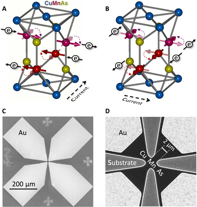
(A) Schematics of the crystal and magnetic structure of the CuMnAs antiferromagnet in which the two opposite magnetic sublattices occupy inversion partner Mn sites. A uniform electrical current (black dashed arrow) generates a nonequilibrium spin polarization of carriers (black electron symbols with spin arrows) with opposite sign at inversion partner Mn sites. The corresponding staggered effective magnetic field efficiently switches the antiferromagnetic moments (reorientation of thick red/purple arrows). (B) Reversible switching is achieved by applying the writing current in the orthogonal direction. (C) Electron microscopy image of the Au contact pads (light regions) of the device. (D) Detailed electron microscopy image of the device with a 2-μm-size central cross structure. Light regions are the apexes of Au contact pads, gray regions are etched down to the GaAs substrate, and black regions are CuMnAs.
To establish the feasibility of extending the writing speed in antiferromagnets to the terahertz band, we compare our ultrashort writing pulse experiments to the results obtained with longer writing pulses in the same device structure. Electron micrographs of the device are shown in Fig. 1 (C and D). We first recall the previously established technique that has enabled the scaling of the writing pulse time τp down to 250 ps, corresponding to the writing speed 1/τp of up to 4 GHz (16, 22). In this scheme, the current pulses are delivered via wire-bonded contacts, and here, τp ~ 100 ps is at the limit achievable with common current pulse setups. A 90° reversible switching is realized in cross-shape bit cells (see Fig. 1, C and D) by alternating current pulses along one of the two orthogonal directions, as shown by white dashed lines on the electron microscopy image of the cell in Fig. 2A. White double arrows depict the corresponding orthogonal Néel vector orientations preferably set by the two current directions. Apart from the reversible switching controlled by alternating the two orthogonal writing currents, earlier studies have also shown that multiple pulses can be applied successively along one writing path, revealing neuron-like multilevel switching characteristics naturally occurring in antiferromagnetic microstructures (14, 16, 24, 25). This has been associated with multidomain reconfigurations (26), and we will exploit the feature also in our picosecond pulse experiments described below.
Fig. 2. Contact and noncontact experimental setup.
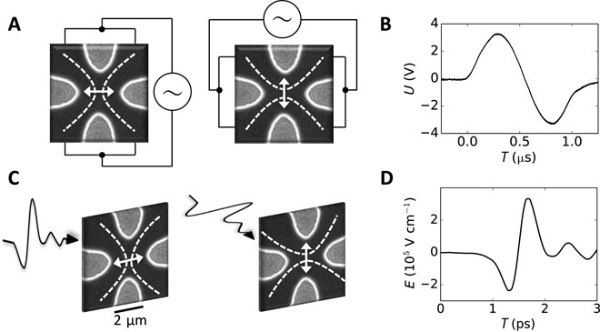
(A) Electron microscopy image of the cross-shape bit cell and schematics of the reversible writing by electrical pulses of two orthogonal current directions delivered via wire-bonded contacts. White dashed lines illustrate electrical current paths, and white double arrows show the corresponding preferred Néel vector orientations. (B) Waveform of the applied microsecond electrical pulses. (C) Schematics of the reversible writing by terahertz electric field transients whose linear polarization can be chosen along two orthogonal directions. (D) Waveform of the applied picosecond radiation pulses.
For our experiments with 1/τp in the terahertz range, we use the same cross-shape bit cell and an analogous experimental setup. However, as shown in Fig. 2C, we use a noncontact technique for generating the ultrashort current pulses in the memory cell to overcome the above limit of common contact-based current pulse setups. To explore reversible writing with pulses of τp ≈ 1 ps, we apply free-space terahertz electromagnetic pulses whose linear polarization can be chosen along two orthogonal directions, as sketched in Fig. 2C. The waveform of the incident electric field transient is plotted in Fig. 2D (for more details, see Materials and Methods) (27). As in the contact writing scheme, white double arrows depict the corresponding orthogonal Néel vector orientations preferably set by the two orthogonal polarizations.
In both contact and noncontact setups, the electrical readout is performed by detecting the antiferromagnetic transverse anisotropic magnetoresistance (AMR) (using a readout current amplitude of 3 × 10⁵ A cm–2), as shown in Fig. 3 (14, 15, 24). Here, the readout current direction is depicted by a white dashed line on the electron microscopy image of the cell. The transverse AMR has opposite signs for the two orthogonal Néel vector directions. The correspondence between the electrical readout signals and the 90° reversible switching of antiferromagnetic domains was confirmed in earlier experiments using x-ray magnetic linear dichroism photoemission electron microscopy (14, 26).
Fig. 3. Comparison of switching by microsecond and picosecond pulses.
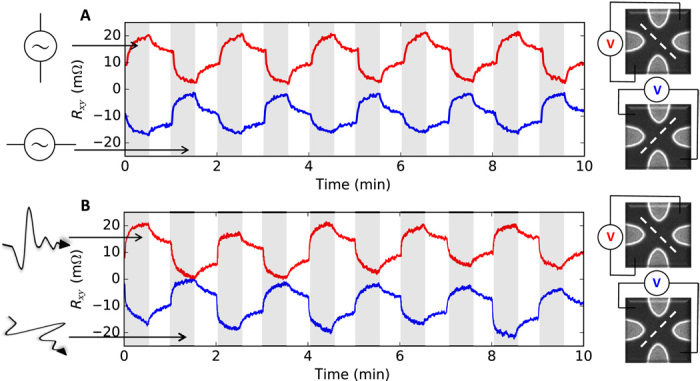
(A) Reversible multilevel switching by 30-s trains of microsecond electrical pulses with a hertz pulse repetition rate, delivered via wire-bonded contacts along two orthogonal directions. The applied writing current density in the 3.5-μm-size CuMnAs/GaAs cell is 3 × 10⁷ A cm–2. Intervals with the pulse trains turned on are highlighted in gray, and the two orthogonal current directions of the trains alternate from one interval to the next. Electrical readout is performed at a 1-Hz rate. Right insets show schematics of the transverse AMR readout. White dashed lines depict readout current paths. (B) Same as (A) for picosecond pulses with a kilohertz pulse repetition rate. The writing current density in the 2-μm-size CuMnAs/GaAs bit cell recalculated from the amplitude of the applied terahertz electric field transient is 2.7 × 10⁹ A cm–2. Electrical readout is performed at an 8-Hz rate.
To confirm the AMR symmetry, we use two electrical detection geometries in which we interchanged the readout current and transverse voltage axes (see Fig. 3). For the AMR, the readout signal flips sign between the two geometries (14). Note that the AMR readout signal in these experiments does not depend on the polarity of the writing current. We also apply a bipolar waveform of the writing pulses in the contact setup to explicitly highlight the correspondence to the noncontact, picosecond pulse measurements (see Fig. 2, B and D). All experiments are performed at room temperature.
Terahertz writing speed experiments
In Fig. 3A, we present measured data for microsecond writing pulses. These were delivered by the contact method in a bit cell fabricated from a 50-nm-thick CuMnAs film deposited on an insulating GaAs substrate. The pulse train of one current direction is turned on for 30 s, and then the train is turned off for 30 s, followed by turning on for 30 s the pulse train with the orthogonal current direction. The data show the phenomenology attributed in the earlier studies to the multilevel switching of the antiferromagnet by the current-induced staggered spin-orbit field (14, 16). The readout signal increases as the successive pulses within a train arrive at the bit cell. The trend reverses when applying the pulse train with the orthogonal current direction, and the overall sign of these reversible switching traces flips between the two readout geometries, consistent with the AMR symmetry.
Note that the readout signal in Fig. 3A partially relaxes after turning the pulse train off. In the Supplementary Materials, we show that no relaxation is observed in this CuMnAs structure when slightly lowering the temperature to 260 K. In general, the stability of the switching signal can be broadly varied by changing the CuMnAs structure parameters (16); examples of stable retention at room temperature in CuMnAs are reported by Wadley et al. (18), and in Mn2Au by Bodnar et al. (19). Data in Fig. 3A were obtained for an applied writing current density j = 3 × 10⁷ A cm–2 and a writing pulse repetition rate of 1 Hz. Wadley et al. (14) and Olejník et al. (16) reported more systematic dependencies of the switching signal on the writing pulse length, repetition rate, and current density in the contact setup.
Remarkably, analogous reversible switching traces, with an initial steep increase of the AMR signal followed by a tendency to saturate, can be written in the same CuMnAs memory cell structure by picosecond pulses, as shown in Fig. 3B. Here, the current density, recalculated from the applied intensity of the terahertz electric field E = 1.1 × 10⁵ V cm–1, was increased to j ≈ 2.7 × 10⁹ A cm–2 for these ultrashort pulses. See below for a detailed discussion of the E to j conversion. The correspondence between the measured data in Fig. 3 (A and B) indicates that for the picosecond pulses, the reversible switching of the antiferromagnet, controlled by the polarization direction of the incident terahertz electric field, is also due to the current-induced staggered spin-orbit field. Note that this switching mechanism allows us to use the electric field transient and that we do not rely on the weak magnetic field component of the radiation (28) or on nonlinear orbital transition effects (29).
Performing a measurement with an isolated single pulse was not feasible in our terahertz setup. However, we emphasize that the writing pulse repetition rate in Fig. 3B was set to 1 kHz, that is, the ratio of pulse delay to pulse length is as large as 109. We also point out that at the millisecond (or longer) range of delays between writing pulses, the change of the signal due to the subsequent pulse in the train is not affected by transient heating effects of the previous pulse and is independent of the delay time (16).
However, to more explicitly highlight the effect of a single picosecond pulse, we increase the current density to j ≈ 2.9 × 10⁹ A cm–2 and further reduce the repetition rate of the writing pulses to 125 Hz and match it closely to the readout repetition rate (100 Hz). The measured data plotted as a function of the pulse number are shown in Fig. 4A. We observe that the initial picosecond pulse accounts for a sizable portion of the total signal generated by the pulse train. Note that the scatter in the measured data is likely of an instrumental origin because of the electrical noise from the laser setup and fluctuations of laser power and beam pointing. In Fig. 4B, we show corresponding measurements with the microsecond pulses, which again highlight the analogous phenomenology of the terahertz speed writing and the slower writing in the multilevel antiferromagnetic bit cell.
Fig. 4. Effects of individual picosecond and microsecond pulses.
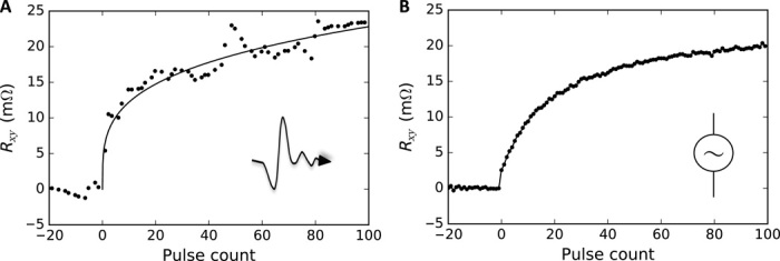
(A) The multilevel memory signal as a function of the number of applied picosecond pulses. The writing current density in the 2-μm-size CuMnAs/GaAs bit cell recalculated from the applied terahertz field amplitude is 2.9 × 10⁹ A cm–2. (B) Same as (A) for the microsecond pulses and an applied writing current density of 3 × 10⁷ A cm–2 in the 3.5-μm-size CuMnAs/GaAs cell.
Determination of terahertz writing current and energy density
The electrical current density generated in our CuMnAs memory cells for a given incident terahertz field could not be directly measured. To obtain the writing current density in the terahertz experiments, and the corresponding Joule energy density, we performed independent numerical simulations and experimental calibration based on sample breakdown measurements. These two alternative theoretical and experimental methods, which we now describe in more detail, provide quantitatively consistent results.
The key input parameter of the numerical simulations is the frequency-dependent dielectric function ε of CuMnAs, whose measurement is shown in Fig. 5A (for details, see Materials and Methods). The data can be accurately fitted with Im ε = σ/ωε0, where the value of the dc conductivity σ = 8 × 10³ ohm− 1 cm− 1 agrees with the value obtained from electrical measurements. Using a transfer matrix formalism (30), we first calculate the electric field inside the 50-nm-thick CuMnAs layer in a layered structure of air/CuMnAs/GaAs without Au electrodes upon incidence of the terahertz field. The amplitude of the electric field in CuMnAs is only 10% of the incident terahertz field value. For the peak incident terahertz field of 105 V cm–1, the calculated current density in the CuMnAs film would be 8 × 10⁷ A cm–2. Experimentally, we did not observe switching by the terahertz field pulses in structures without Au electrodes, which implies that this current density is below the switching threshold for picosecond pulses.
Fig. 5. Electric field simulations in the device.
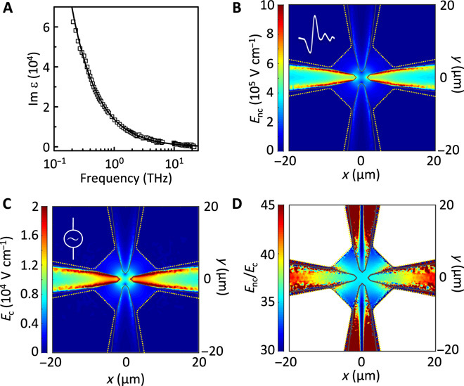
(A) Measured frequency-dependent imaginary part of the dielectric function (squares) and fitted expression Im ε = σ/ωε0 (line) with the dc conductivity σ = 8 × 10³ ohm− 1 cm− 1. (B) Numerical simulation of the electric field distribution in the device in the noncontact setup for a peak incident terahertz field of 105 V cm–1 polarized along the y axis. (C) Same as (B) in the contact setup for a voltage of 7 V applied between the top and bottom Au contacts. (D) Ratio of the electric fields in (B) and (C).
We observed switching in devices with Au electrodes that strongly modify the incident terahertz field in the CuMnAs cross region. This is confirmed by numerical simulations of the terahertz electric field distribution (see Materials and Methods) that also took the measured dielectric function of CuMnAs at 1-THz frequency as an input and whose results are plotted in Fig. 5 (B and C). Here, we compare, side by side, the electric field distribution in the cross structure for the typical peak incident terahertz field of 105 V cm–1 used in the noncontact picosecond pulse experiment (Fig. 5B) with the field distribution for the typical voltage of 7 V applied in the contact setup for nanosecond switching pulses (Fig. 5C). For clarity, we also plot in Fig. 5D the ratio of the fields in the two setups. The corresponding current densities in the center of the CuMnAs cross are ≈2 × 10⁹ A cm–2 and 6 × 10⁷ A cm–2, respectively, which implies that the simulated writing energy density, , remains constant when increasing the writing speed 1/τp from gigahertz to terahertz.
We now proceed to the experimental calibration of the writing current and energy density in the terahertz field experiments. First, we show in Fig. 6 (A and B) measurements in devices with central cross widths of 1, 2, and 3 μm, and with otherwise the same geometry of the Au electrodes (Fig. 6A) and approximately the same resistance of the devices. The terahertz-induced switching signal plotted as a function of the incident terahertz peak field depends on the size of the cross (Fig. 6B). We again ascribe this observation to the Au electrodes. As shown previously by Novitsky et al. (31) and McMahon et al. (32), and consistent with the above simulations in Fig. 5B, a terahertz field polarized parallel to the electrode drives currents inside the metal, thereby inducing charges of opposite sign on opposite electrode apexes. These charges, and the resulting voltage across the inner device, govern the current in our CuMnAs crosses. At a given incident terahertz peak field, the current flowing through the three different crosses is comparable and, correspondingly, the current density scales up with decreasing width of the crosses. This is consistent with our observation of increasing AMR signal with decreasing cross size (Fig. 6B). When we accordingly rescale the data in Fig. 6B by the cross sizes, as shown in the inset, the three curves fall on top of each other, in agreement with the expected phenomenology for the current-induced switching.
Fig. 6. Switching energy calibration.
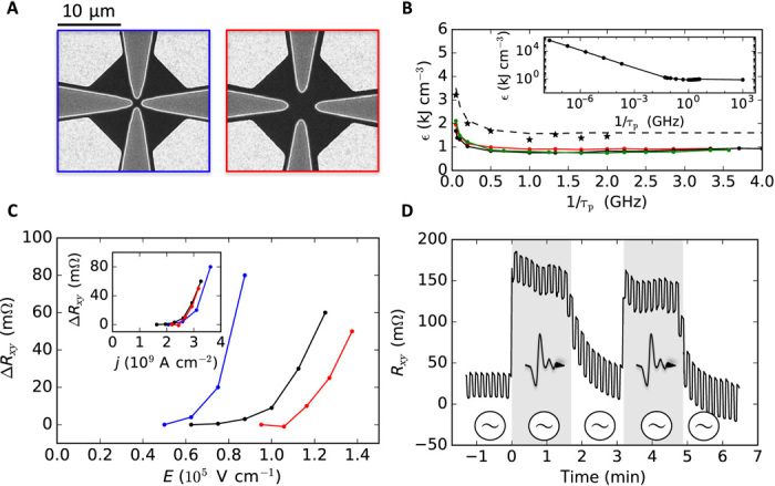
(A) Electron microscopy images of the 1- and 3-μm-size devices. Light regions are Au contact pads, gray regions are etched down to the GaAs substrate, and black regions are CuMnAs. (B) Magnitude of the switching signal as a function of the terahertz field amplitude (main panel) and of the converted current density (inset) for 1-, 2-, and 3-μm-size devices (blue, black, and red dots, respectively). (C) Writing energy density (black, red, and green dots), ϵ = j2τp/σ, required to obtain a 1-milliohm switching signal as a function of the writing speed in the linear scale (main plot) and in the log-log scale (inset). All data points, except for the point at = 1 THz in the inset, are obtained from the contact measurements. The point at = 1 THz in the inset is from the noncontact measurement using the E to j conversion based on the breakdown energy (see text). Black dots in the main plot correspond to 2-μm-size, red to 3-μm-size, and green to 4-μm-size CuMnAs/GaAs bit cells. Black star symbols and dashed line represent the limiting breakdown energy density. (D) Contact writing by 200-ms pulses of current density 1 × 10⁷ A cm–2 (white intervals) and the contact writing superimposed on the noncontact writing by a train of picosecond pulses with a kilohertz repetition rate and a terahertz field amplitude corresponding to an additional current density of approximately 1.6 × 10⁹ A cm–2 (gray intervals). Data were measured in a 10-μm-size CuMnAs/Si bit cell.
We point out that charges at the electrode apexes are also induced when a voltage is applied between opposite electrodes in the contact experiments. Therefore, similar field distributions in the cross region are formed for the contact and noncontact field applications, differing only by a global scaling factor. This is confirmed by our simulations in Fig. 5. We take advantage of this notion to experimentally calibrate the terahertz current. As detailed in the Supplementary Materials, we determine in the contact experiments the critical absorbed Joule energy density leading to device damage for 1/τp up to 4 GHz. Because the energy already saturates in the gigahertz range, extrapolation to the terahertz writing speed is straightforward and enables determination of the scaling factor between the incident peak field and the resulting peak current density in the CuMnAs cross.
The calibration procedure allows us to plot the characteristic Joule energy density required to obtain a reference switching signal of 1 milliohm up to the terahertz range, as shown in the inset of Fig. 6C. We find a steeply decreasing with increasing 1/τp below the megahertz range to a saturated value of in the gigahertz range (see also main plot of Fig. 6C) that extends to the terahertz writing speed. This demonstrates that, in agreement with the above numerical simulations, current-induced switching at the terahertz writing speed is as energy-efficient as at the gigahertz speed. Note that a small increase of the writing current amplitude induces a large increase of the signal, as shown in Fig. 6B; our conclusions on the writing energy are therefore independent of the particular choice of the reference signal.
The Joule energy leading to device damage and the energy required for switching are separated by approximately a factor of 2 in both the gigahertz and terahertz writing speed range. The vicinity of the breakdown condition in our switching experiments is favorable from the perspective of the above current calibration procedure because it limits potential inaccuracies of the procedure. Simultaneously, the breakdown margin is sufficiently large, allowing us to demonstrate tens of thousands of reversible write-read cycles without any notable wear-out of our experimental devices (16).
Finally Fig. 6D, we demonstrate that one antiferromagnetic multilevel bit cell can be simultaneously addressed by the noncontact terahertz speed writing and the contact lower speed writing. For the illustration, we choose a CuMnAs/Si bit cell and plot the readout signal when applying 200-ms pulses of j = 1 × 10⁷ A cm–2 by the contact method with alternating orthogonal current path directions and a 5 s delay between pulses. After 15 switchings, we added the noncontact writing in the form of a 90-s-long train of picosecond pulses with a kilohertz repetition rate and a current density j ≈ 1.6 × 10⁹ A cm–2. The noncontact picosecond pulses induce an additional switching of the multilevel cell with the superimposed smaller switching signals controlled by the contact pulses.
DISCUSSION
We will now discuss our results in the broader context of writing of magnetic memories. The above presented data illustrate that we have pushed the electrical spin-torque switching, which drives current research and development of magnetic memories, to the terahertz writing speed range. At the gigahertz writing speed, the antiferromagnetic CuMnAs bit cells are written by current densities j ~ 108 A cm–2 (16), which are comparable to ferromagnetic spin-orbit torque MRAMs (10, 11). The associated writing Joule energy density, kJ cm–3, in our antiferromagnetic devices also matches the energy density at a gigahertz writing speed in ferromagnetic spin-transfer torque (9, 33) or spin-orbit torque (10) memory devices.
For the terahertz writing speed, the applied current density in our antiferromagnetic devices increases only to a value of the order of j ~ 109 A cm–2, and the writing energy remains the same as for the gigahertz writing speed. This makes antiferromagnets realistic candidate materials for electrically controlled memory devices in the terahertz band.
The result is in marked contrast to ferromagnets where the projected current and energy of the writing would increase by three orders of magnitude from the gigahertz to the terahertz writing speed. For 1/τp up to a gigahertz, the current density required for switching in spin-orbit torque memories fabricated in the common ferromagnetic transition metal structures is ~108 A cm–2 and only weakly deviates from the steady current limit because of the heat-assisted magnetization reversal (10). This current density corresponds to an effective field Heff ~ 10 to 100 mT required for the switching of ferromagnetic moments over the magnetic energy barrier (12). However, when 1/τp is above the gigahertz threshold, the steady current limit Heff is no longer sufficient for switching because τp becomes comparable to or smaller than the limiting magnetization reorientation time scale. This is given by 1/f, where is the ferromagnetic resonance frequency. To keep f in scale with 1/τp, the effective writing field, and therefore j, has to increase linearly with 1/τp above the gigahertz threshold (10). In particular, f reaches 1 THz at about 30 T, and the switching current density linearly extrapolated to the terahertz writing speed would be ~1011 A cm–2 in the ferromagnetic spin-orbit torque devices. This also means that although the writing energy ~j2τp initially drops down with increasing 1/τp, in ferromagnets, it starts to increase linearly with 1/τp above the gigahertz threshold. A terahertz writing speed would then require energy three orders of magnitude higher than that required for the gigahertz writing speed used in present MRAM devices. With these basic physical limitations, the current-induced spin-orbit torque switching has not been pushed in ferromagnetic MRAMs to 1/τp far exceeding 5 GHz (10, 11).
On the other hand, the antiferromagnetic resonance frequency is exchange-enhanced and scales as , which puts it in the terahertz range (34). Here, HE is the interspin sublattice exchange field and HA stands for the anisotropy field (in the absence of externally applied fields). This enhancement of the antiferromagnetic resonance frequency and, correspondingly, of the threshold writing speed is due to canting of the antiferromagnetic spin sublattices when brought out of equilibrium.
A uniform magnetic field as required for switching is also exchange-enhanced in antiferromagnets and scales as , which typically takes it into the tens of Tesla range, inaccessible in microelectronics. However, we exploited the current-induced staggered field that is commensurate with the staggered Néel order, that is, which flips sign at the opposite spin sublattices (see Fig. 1). Although dynamics induced by this staggered field still includes canting of the antiferromagnetic spin sublattices and is thus exchange-enhanced, the amplitude of the staggered field required for switching is only of the order of the anisotropy field, as discussed in detail by Železný et al. (15) and Roy et al. (21). In the antiferromagnet under the current-induced staggered field, the exchange enhancement factor of the switching field amplitude is, therefore, absent. This principle allows antiferromagnets to reach terahertz writing speeds at accessible fields and energies, as confirmed by our experiments and predicted in earlier numerical atomistic spin dynamics simulations (21).
Considering only the role of the staggered effective magnetic field in a model scenario of coherent switching over an anisotropy field barrier, the writing field and corresponding writing current should remain constant and the energy should then decrease with increasing writing speed down to the terahertz range. However, we observe in our experimental structures that the trend changes between megahertz and gigahertz, beyond which the writing energy remains approximately constant. Experiments in the contact setup, discussed in the Supplementary Materials, confirm that heating effects play an important role in switching and explain why the writing energy saturates.
Apart from requiring approximately the same energy of the writing current pulses in the whole range of 1/τp from ~100 MHz to the terahertz value, the switching at the terahertz writing speed remains reversible, with the switching direction determined by the direction of the applied pulses. It suggests that a significant reorientation of the antiferromagnetic moments occurs while the terahertz pulse is on, that is, at a picosecond (or shorter) time scale. This is again consistent with earlier numerical simulations of the antiferromagnetic dynamics under the applied staggered field, showing picosecond-scale switching times by picosecond writing electrical pulses (21). Experimentally, however, it needs to be confirmed in future experiments combining picosecond-scale writing with a comparable readout scale. These experiments will provide a time-resolved physical picture of the switching mechanism and will open the prospect of an ultrafast complete write-read cycle in antiferromagnetic memories. In an earlier work by several of us (35), we have already demonstrated an initial step in this direction by detecting the Néel vector direction in CuMnAs in a femtosecond laser setup by magnetic linear dichroism, which is the optical counterpart of the AMR.
As a concluding remark, we point out that a terahertz speed memory, whether realized in antiferromagnets or another alternative system that may be discovered in the future, is only one of the many components that need to be developed to make true terahertz electronics and information technologies a realistic prospect. In the meantime, however, the ultrafast writing of antiferromagnetic bit cells can be potentially exploitable without separate terahertz speed processors. The multilevel neuron-like characteristics of our devices, seen in Fig. 3, allow the integration of memory and logic within the antiferromagnetic bit cell. An example of the combined memory-logic has already been demonstrated in earlier GHz writing speed experiments by showing a pulse counter functionality in the CuMnAs device (16). Future low-noise experiments with terahertz writing pulses and repetition rates spanning a broad range up to terahertz will establish the feasibility and versatility of this autonomous terahertz memory-logic concept, built within the antiferromagnetic bit cells, that requires no separate processor to perform the terahertz speed logic operation.
MATERIALS AND METHODS
CuMnAs growth
The CuMnAs film was grown on GaAs(001) or Si(001) by molecular beam epitaxy at a substrate temperature of 220°C. X-ray diffraction measurements showed that the films have the tetragonal Cu2Sb structure (space group P4/nmm). The film and substrate follow the epitaxial relationship CuMnAs (001)[100]∥GaAs(001)[110] or Si(001)[110]. The CuMnAs film thickness is 50 nm. Magnetic measurements confirmed that the CuMnAs film is a compensated antiferromagnet. The Néel temperature is 480 K, and dc conductivity is 8 × 10³ ohm− 1 cm− 1.
Lithography
Microfabrication of our CuMnAs cross-shape cells was done using electron beam lithography and reactive ion etching. We used metal masks prepared by lift-off method directly on the surface of CuMnAs films to define the pattern and protect the CuMnAs layer during the reactive ion etching step. We have developed fabrication recipes (consisting of oxide removal just before insertion to the contact pad deposition chamber) which enable us to reduce the degree of oxidation of the CuMnAs surface below contact pads, which was necessary to avoid otherwise non-negligible and uncontrolled contact resistance.
Experimental setup for terahertz field pulses
For the terahertz measurements, intense electromagnetic radiation fields (at ~1 THz) were generated by optical rectification of laser pulses (center wavelength, 800 nm; pulse duration, 350 fs; pulse energy, 4 mJ; repetition rate, 1 kHz) from an amplified laser system in a 1.3 mol percent MgO-doped stoichiometric LiNbO3 crystal (LN) with the tilted pulse front technique (36, 37). To determine the electric field component of the radiation, a (001)-oriented quartz crystal (thickness, 50 μm) was placed at the sample position, where it induced a transient birefringence through the linear electro-optic effect. The birefringence and, therefore, the field were sampled step by step by a variably delayed optical laser pulse (pulse energy, 2 nJ; central wavelength, 800 nm; pulse duration, 8 fs; repetition rate, 80 MHz) co-propagating through the electro-optic material (27). The electric field strength at the focus was calibrated by measuring the pulse energy by a power meter (Gentec THz-B) and the terahertz beam waist by transmission through an aperture. For the terahertz writing experiments, the sample was placed in the focus of the normally incident radiation beam. The two perpendicular polarization settings of the beam were realized by a wire grid polarizer.
Measurement of frequency-dependent dielectric function of CuMnAs
Terahertz dielectric spectra of CuMnAs (50 nm)/GaAs (0.5 mm) were measured by using two custom-made spectrometers. First, transmission measurements of the film were performed in a standard time-domain terahertz spectroscopy setup (0.15 to 3 THz) based on a femtosecond laser oscillator [see details in the study of Kužel et al. (38)]. The value of the GaAs substrate thickness, used for the retrieval of the complex refractive index and dielectric function of the film, was refined by using internal Fabry-Perot reflections in the substrate, which are resolved in time and form distinct terahertz pulses separated in time (39). In this way, the substrate thickness can be estimated with a precision of 200 nm, which is essential for an accurate determination of the phase change during the propagation through the thin film sample. Subsequently, a homemade terahertz air-based photonics setup with air-based coherent detection scheme (40) was used to determine the complex dielectric spectra of the sample in the frequency range of 1 to 23 THz. To this aim, the spectrum of the GaAs substrate was determined using the same experimental setup, and the substrate thickness determined in previous experiments was used. This experiment was powered by a femtosecond amplifier (Spectra-Physics, ACE) delivering 35-fs-long pulses at 5-kHz repetition rate; the experiment required 0.5-mJ energy per pulse.
Simulations of the terahertz electric field distribution in the device
The terahertz and dc electric field distributions in the CuMnAs device were numerically simulated using a finite element method (COMSOL Multiphysics 5.1). In particular, for the terahertz case, we use the “Electromagnetic Waves, Frequency Domain Interface” of the RF Module to solve the time-harmonic wave equation for sinusoidally time-varying fields. The incident terahertz electric field was modeled as a Gaussian beam propagating along the surface normal (z axis) with width of 900 μm, frequency of 1 terahertz, and linear polarization along the in-plane y axis. The dielectric function of CuMnAs was taken from experiment (see above and main text). For Au, we used a Drude model dielectric function, Re ε = 9 × 10⁴ and Im ε = 7 × 10⁵. To calculate the dc electric field, we used the AC/DC module, solving the Laplace equation for the electric potential. The device geometry is modeled in three dimensions (3D), with its full lateral size in the x and y directions. To reduce the computational cost and limit the number of mesh elements, which becomes particularly problematic for geometries with large aspect ratios as in the case of two thin adjacent films, special care has to be taken in modeling the geometry along the z direction. For this reason, we model the CuMnAs layer using the “Transition Boundary Condition,” which calculates the drop in the transmitted electric field based on the skin depth and the complex-valued permittivity and assuming a thickness of 50 nm, without the need to model the field inside the layer. The gold contacts were instead modeled as 3D thin films with a thickness of 100 nm using a 10× mesh scaling along the lateral direction. We chose a simulation volume large enough to avoid artifacts arising from reflections at the boundaries of the simulation volume. Similarly, we chose maximum and minimum element sizes of the mesh to not exceed λ/6 and to properly resolve and model the curvatures of the gold pads, respectively. Proper modeling of the edges in the center of the device is crucial to avoid giant artificial field enhancements occurring at metallic point-like features in the geometry.
Supplementary Material
Acknowledgments
Funding: This work was supported in part by the Ministry of Education of the Czech Republic (grants LM2015087 and LNSM-LNSpin), the Grant Agency of the Czech Republic (grant 14-37427G), the EU FET Open RIA (grant 766566), the University of Nottingham Engineering and Physical Sciences Research Council Impact Acceleration Account (grant EP/K503800/1), the Alexander von Humboldt Foundation, European Research Council (ERC) Synergy Grant SC2 No. 610115, Transregional Collaborative Research Center (SFB/TRR) 173 SPIN+X, ERC Consolidator Grant TERAMAG No. 681917, Engineering and Physical Sciences Research Council grant EP/P019749/1, and the Swiss National Science Foundation (grant 200020_172775). P.W. acknowledges support from the Royal Society through a Royal Society University Research Fellowship. Author contributions: K.O., T.S., T.K., P.G., P.W., J.W., P.N., and T.J. conceived and designed experiments. K.O., T.S., Z.K., M.B., and P.K. performed experiments. K.O., T.S., T.K., P.K., J.S., and T.J. analyzed data. V.N. and R.P.C. contributed materials. M.M. performed numerical simulations. K.O., T.K., and T.J. wrote the paper. Competing interests: J.W., T.J., V.N., R.P.C., P.W., and K.O. are inventors on a patent application related to this work filed by Hitachi Ltd., Institute of Physics of Czech Academy of Sciences, and University of Nottingham (application no. EP17197856, filed 23 October 2017). All other authors declare no competing interests. Data and materials availability: All data needed to evaluate the conclusions in the paper are present in the paper and/or the Supplementary Materials. Additional data related to this paper may be requested from the authors.
SUPPLEMENTARY MATERIALS
Supplementary material for this article is available at http://advances.sciencemag.org/cgi/content/full/4/3/eaar3566/DC1
section S1. Terahertz current calibration
section S2. Temperature dependence of the relaxation
section S3. Heat-assisted nature of the reversible switching
fig. S1. Comparison of switching at 300 and 260 K.
fig. S2. Device temperature with the pulse on.
REFERENCES AND NOTES
- 1.Chappert C., Fert A., Van Dau F. N., The emergence of spin electronics in data storage. Nat. Mater. 6, 813–823 (2007). [DOI] [PubMed] [Google Scholar]
- 2.Brataas A., Kent A. D., Ohno H., Current-induced torques in magnetic materials. Nat. Mater. 11, 372–381 (2012). [DOI] [PubMed] [Google Scholar]
- 3.Kent A. D., Worledge D. C., A new spin on magnetic memories. Nat. Nanotechnol. 10, 187–191 (2015). [DOI] [PubMed] [Google Scholar]
- 4.Waldrop M. M., The chips are down for Moore’s law. Nature 530, 144–147 (2016). [DOI] [PubMed] [Google Scholar]
- 5.Ralph D. C., Stiles M. D., Spin transfer torques. J. Magn. Magn. Mater. 320, 1190–1216 (2008). [Google Scholar]
- 6.Chernyshov A., Overby M., Liu X., Furdyna J. K., Lyanda-Geller Y., Rokhinson L. P., Evidence for reversible control of magnetization in a ferromagnetic material by means of spin-orbit magnetic field. Nat. Phys. 5, 656–659 (2009). [Google Scholar]
- 7.Miron I. M., Garello K., Gaudin G., Zermatten P.-J., Costache M. V., Auffret S., Bandiera S., Rodmacq B., Schuhl A., Gambardella P., Perpendicular switching of a single ferromagnetic layer induced by in-plane current injection. Nature 476, 189–193 (2011). [DOI] [PubMed] [Google Scholar]
- 8.Liu L., Pai C.-F., Li Y., Tseng H. W., Ralph D. C., Buhrman R. A., Spin-torque switching with the giant spin Hall effect of tantalum. Science 336, 555–558 (2012). [DOI] [PubMed] [Google Scholar]
- 9.Bedau D., Liu H., Sun J. Z., Katine J. A., Fullerton E. E., Mangin S., Kent A. D., Spin-transfer pulse switching: From the dynamic to the thermally activated regime. Appl. Phys. Lett. 97, 262502 (2010). [Google Scholar]
- 10.Garello K., Avci C. O., Miron I. M., Baumgartner M., Ghosh A., Auffret S., Boulle O., Gaudin G., Gambardella P., Ultrafast magnetization switching by spin-orbit torques. Appl. Phys. Lett. 105, 212402 (2014). [Google Scholar]
- 11.Prenat G., Jabeur K., Vanhauwaert P., Pendina G. D., Oboril F., Bishnoi R., Ebrahimi M., Lamard N., Boulle O., Garello K., Langer J., Ocker B., Cyrille M. C., Gambardella P., Tahoori M., Gaudin G., Ultra-fast and high-reliability SOT-MRAM: From cache replacement to normally-off computing. IEEE Trans. Multi-Scale Comput. Syst. 2, 49–60 (2016). [Google Scholar]
- 12.Baumgartner M., Garello K., Mendil J., Avci C. O., Grimaldi E., Murer C., Feng J., Gabureac M., Stamm C., Acremann Y., Finizio S., Wintz S., Raabe J., Gambardella P., Spatially and time-resolved magnetization dynamics driven by spin-orbit torques. Nat. Nanotechnol. 12, 980–986 (2017). [DOI] [PubMed] [Google Scholar]
- 13.Marrows C. H., Perspectives: Addressing an antiferromagnetic memory. Science 351, 558–559 (2016). [DOI] [PubMed] [Google Scholar]
- 14.Wadley P., Howells B., Žlezný J., Andrews C., Hills V., Campion R. P., Novák V., Olejnik K., Maccherozzi F., Dhesi S. S., Martin S. Y., Wagner T., Wunderlich J., Freimuth F., Mokrousov Y., Kuneš J., Chauhan J. S., Grzybowski M. J., Rushforth A. W., Edmonds K. W., Gallagher B. L., Jungwirth T., Electrical switching of an antiferromagnet. Science 351, 587–590 (2016). [DOI] [PubMed] [Google Scholar]
- 15.Železný J., Gao H., Výborný K., Zemen J., Mašek J., Manchon A., Wunderlich J., Sinova J., Jungwirth T., Relativistic Néel-order fields induced by electrical current in antiferromagnets. Phys. Rev. Lett. 113, 157201 (2014). [DOI] [PubMed] [Google Scholar]
- 16.Olejník K., Schuler V., Marti X., Novák V., Kašpar Z., Wadley P., Campion R. P., Edmonds K. W., Gallagher B. L., Garces J., Baumgartner M., Gambardella P., Jungwirth T., Antiferromagnetic CuMnAs multi-level memory cell with microelectronic compatibility. Nat. Commun. 8, 15434 (2017). [DOI] [PMC free article] [PubMed] [Google Scholar]
- 17.Jungwirth T., Marti X., Wadley P., Wunderlich J., Antiferromagnetic spintronics. Nat. Nanotechnol. 11, 231–241 (2016). [DOI] [PubMed] [Google Scholar]
- 18.P. Wadley, S. Reimers, M. J. Grzybowski, C. Andrews, M. Wang, B. L. Gallagher, R. P. Campion, K. W. Edmonds, S. S. Dhesi, V. Novák, J. Wunderlich, T. Jungwirth, Current-polarity dependent manipulation of antiferromagnetic domains. http://arxiv.org/abs/1711.05146 (2017). [DOI] [PubMed]
- 19.Bodnar S. Y., Šmejkal L., Turek I., Jungwirth T., Gomonay O., Sinova J., Sapozhnik A. A., Elmers H.-J., Kläui M., Jourdan M., Writing and reading antiferromagnetic Mn2Au: Néel spin-orbit torques and large anisotropic magnetoresistance. Nat. Commun. 9, 348 (2018). [DOI] [PMC free article] [PubMed] [Google Scholar]
- 20.M. Meinert, D. Graulich, T. Matalla-Wagner, Key role of thermal activation in the electrical switching of antiferromagnetic Mn2Au. http://arxiv.org/abs/1706.06983 (2017).
- 21.Roy P. E., Otxoa R. M., Wunderlich J., Robust picosecond writing of a layered antiferromagnet by staggered spin-orbit fields. Phys. Rev. B 94, 014439 (2016). [Google Scholar]
- 22.Wadley P., Novák V., Campion R., Rinaldi C., Martí X., Reichlová H., Železný J., Gazquez J., Roldan M., Varela M., Khalyavin D., Langridge S., Kriegner D., Máca F., Mašek J., Bertacco R., Holý V., Rushforth A., Edmonds K., Gallagher B., Foxon C., Wunderlich J., Jungwirth T., Tetragonal phase of epitaxial room-temperature antiferromagnet CuMnAs. Nat. Commun. 4, 2322 (2013). [DOI] [PubMed] [Google Scholar]
- 23.Železný J., Gao H., Manchon A., Freimuth F., Mokrousov Y., Zemen J., Mašek J., Sinova J., Jungwirth T., Spin-orbit torques in locally and globally noncentrosymmetric crystals: Antiferromagnets and ferromagnets. Phys. Rev. B 95, 014403 (2017). [Google Scholar]
- 24.Kriegner D., Výborný K., Olejník K., Reichlová H., Novák V., Marti X., Gazquez J., Saidl V., Němec P., Volobuev V. V., Springholz G., Holý V., Jungwirth T., Multiple-stable anisotropic magnetoresistance memory in antiferromagnetic MnTe. Nat. Commun. 7, 11623 (2016). [DOI] [PMC free article] [PubMed] [Google Scholar]
- 25.Fukami S., Zhang C., DuttaGupta S., Kurenkov A., Ohno H., Magnetization switching by spin–orbit torque in an antiferromagnet–ferromagnet bilayer system. Nat. Mater. 15, 535–541 (2016). [DOI] [PubMed] [Google Scholar]
- 26.Grzybowski M. J., Wadley P., Edmonds K. W., Beardsley R., Hills V., Campion R. P., Gallagher B. L., Chauhan J. S., Novák V., Jungwirth T., Maccherozzi F., Dhesi S. S., Imaging current-induced switching of antiferromagnetic domains in CuMnAs. Phys. Rev. Lett. 118, 057701 (2017). [DOI] [PubMed] [Google Scholar]
- 27.Sajadi M., Wolf M., Kampfrath T., Terahertz-field-induced optical birefringence in common window and substrate materials. Opt. Express 23, 28985–28992 (2015). [DOI] [PubMed] [Google Scholar]
- 28.Kampfrath T., Sell A., Klatt G., Pashkin A., Mährlein S., Dekorsy T., Wolf M., Fiebig M., Leitenstorfer A., Huber R., Coherent terahertz control of antiferromagnetic spin waves. Nat. Photonics 5, 31–34 (2011). [Google Scholar]
- 29.Baierl S., Hohenleutner M., Kampfrath T., Zvezdin A. K., Kimel A. V., Huber R., Mikhaylovskiy R. V., Nonlinear spin control by terahertz-driven anisotropy fields. Nat. Photonics 10, 715–718 (2016). [Google Scholar]
- 30.R. Jacobsson, in Progress in Optics, E. Wolf, Ed. (North-Holland, 1965), chap. 5, pp. 250–255. [Google Scholar]
- 31.Novitsky A., Ivinskaya A. M., Zalkovskij M., Malureanu R., Jepsen P. U., Lavrinenko A. V., Non-resonant terahertz field enhancement in periodically arranged nanoslits. J. Appl. Phys. 12, 074318 (2012). [Google Scholar]
- 32.McMahon J. M., Gray S. K., Schatz G. C., Fundamental behavior of electric field enhancements in the gaps between closely spaced nanostructures. Phys. Rev. B 83, 115428 (2011). [Google Scholar]
- 33.Bedau D., Liu H., Bouzaglou J.-J., Kent A. D., Sun J. Z., Katine J. A., Fullerton E. E., Mangin S., Ultrafast spin-transfer switching in spin valve nanopillars with perpendicular anisotropy. Appl. Phys. Lett. 96, 022514 (2010). [Google Scholar]
- 34.Kittel C., Theory of antiferromagnetic resonance. Phys. Rev. 82, 565 (1951). [Google Scholar]
- 35.Saidl V., Němec P., Wadley P., Hills V., Campion R. P., Novák V., Edmonds K. W., Maccherozzi F., Dhesi S. S., Gallagher B. L., Trojánek F., Kuneš J., Železný J., Malý P., Jungwirth T., Optical determination of the Néel vector in a CuMnAs thin-film antiferromagnet. Nat. Photonics 11, 91–96 (2017). [Google Scholar]
- 36.Hirori H., Doi A., Blanchard F., Tanaka K., Single-cycle terahertz pulses with amplitudes exceeding 1 MV/cm generated by optical rectification in LiNbO3. Appl. Phys. Lett. 98, 091106 (2011). [Google Scholar]
- 37.Hebling J., Almási G., Kozma I. Z., Velocity matching by pulse front tilting for large-area THz-pulse generation. Opt. Express 10, 1161–1166 (2002). [DOI] [PubMed] [Google Scholar]
- 38.Kužel P., Němec H., Kadlec F., Kadlec C., Gouy shift correction for highly accurate refractive index retrieval in time-domain terahertz spectroscopy. Opt. Express 18, 15338–15348 (2010). [DOI] [PubMed] [Google Scholar]
- 39.Kadlec C., Kadlec F., Němec H., Kužel P., Schubert J., Panaitov G., High tunability of the soft mode in strained SrTiO3/DyScO3 multilayers. J. Phys. Condens. Matter 21, 115902 (2009). [DOI] [PubMed] [Google Scholar]
- 40.Karpowicz N., Dai J., Lu X., Chen Y., Yamaguchi M., Zhao H., Zhang X. C., Zhang L., Zhang C., Price-Gallagher M., Fletcher C., Mamer O., Lesimple A., Johnson K., Coherent heterodyne time-domain spectrometry covering the entire “terahertz gap”. Appl. Phys. Lett. 92, 011131 (2008). [Google Scholar]
Associated Data
This section collects any data citations, data availability statements, or supplementary materials included in this article.
Supplementary Materials
Supplementary material for this article is available at http://advances.sciencemag.org/cgi/content/full/4/3/eaar3566/DC1
section S1. Terahertz current calibration
section S2. Temperature dependence of the relaxation
section S3. Heat-assisted nature of the reversible switching
fig. S1. Comparison of switching at 300 and 260 K.
fig. S2. Device temperature with the pulse on.