Abstract
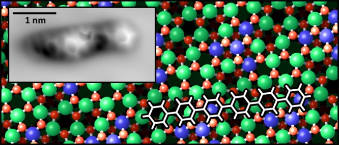
The performance of an organic semiconductor device is critically determined by the geometric alignment, orientation, and ordering of the organic molecules. Although an organic multilayer eventually adopts the crystal structure of the organic material, the alignment and configuration at the interface with the substrate/electrode material are essential for charge injection into the organic layer. This work focuses on the prototypical organic semiconductor para-sexiphenyl (6P) adsorbed on In2O3(111), the thermodynamically most stable surface of the material that the most common transparent conducting oxide, indium tin oxide, is based on. The onset of nucleation and formation of the first monolayer are followed with atomically resolved scanning tunneling microscopy and noncontact atomic force microscopy (nc-AFM). Annealing to 200 °C provides sufficient thermal energy for the molecules to orient themselves along the high-symmetry directions of the surface, leading to a single adsorption site. The AFM data suggests an essentially planar adsorption geometry. With increasing coverage, the 6P molecules first form a loose network with a poor long-range order. Eventually, the molecules reorient into an ordered monolayer. This first monolayer has a densely packed, well-ordered (2 × 1) structure with one 6P per In2O3(111) substrate unit cell, that is, a molecular density of 5.64 × 1013 cm–2.
Keywords: indium oxide, sexiphenyl, organic molecules, atomic force microscopy, scanning tunneling microscopy, adsorption site, monolayer
Introduction
Transparent conducting oxides, such as ZnO, CdO, SnO2, Ga2O3, and In2O3, uniquely combine transparency in the visible range of light with electric conductivity as wide-band-gap semiconductors (fundamental band gap >2 eV).1 In the case of In2O3 (band gap of ∼2.9 eV, see ref (2) for an overview), the intrinsic free-electron concentration at room temperature (RT) is already 1019 cm–3, see ref (3), and can be further enhanced by doping. One of the most widely used dopants is tin (indium tin oxide, ITO), which makes the material almost metal-like in terms of its conductivity while maintaining its optical transparency. ITO is extensively used as an electrode material in light-emitting diodes (LEDs), solar cells, and liquid-crystal displays. Besides their leading role as a transparent electrode material, In2O3 and ITO are also used, for example, as sensor materials to detect gases.4,5 In this work, we use undoped In2O3 single crystals as a model system; in our previous work, we have established that the surfaces of ITO(111) and In2O3(111) are very similar.6,7
In the late 1990s, one of the first blue organic light-emitting diodes (OLEDs) was fabricated from the organic semiconductor para-sexiphenyl with ITO as the anode material.8,9 Today, 6P is known as a model molecule for use in organic devices with a high quantum yield and chemical stability adequate for device technology. The pure powder material is suitable to be handled in an ultrahigh vacuum (UHV) environment and can be sublimed at ∼210 °C. In its crystalline form, at least three bulk structures have been reported for different temperature ranges.10,11 The most commonly observed β-phase (formed at RT) is monoclinic with space group P21/a, two molecules per unit cell, and lattice parameters of a = 0.8091 nm, b = 0.5568 nm, c = 2.6241 nm, and β = 98.17°. The 6P molecules have their long axes parallel to each other but are inclined by 17° to the c-axis of the unit cell.11 In a plane perpendicular to the molecular long axis, that is, roughly 6P(001) or the top view of an upright-standing layer, a herringbone arrangement is formed of alternatingly tilted molecular planes in adjacent 6P(203̅) lattice planes. The phenyl rings of the β-phase are considered to be planar, that is, not twisted. The low-temperature α-phase (110 K) was argued to be very similar to the β-phase but featuring twisted molecules.10,11 Recently, a γ-phase was observed at a growth temperature of 160 °C with small variations in the lattice parameters compared to those of the β-phase and with molecules parallel to the c-axis.11
The onset of crystalline growth of 6P supported on surfaces and its geometric and electronic properties have been studied extensively on numerous noble metals, on surface oxides including the (2 × 1)O reconstruction of Cu(110) and Ni(110), and on a few bulk insulators12,13 and oxides, mainly rutile TiO2(110).14−16 Oxides are often (but not always correctly) assumed to interact weakly (as compared with metals) with such organic compounds, which should, in a first approximation, result in densely packed structures of tilted and/or upright-standing molecules, where the π-overlap among the molecules is maximized and the surface is only slightly wetted. However, even on TiO2(110), a wetting layer of flat-lying but tilted molecules was observed, where the molecules were aligned in the [001] direction in a (very likely) commensurate formation.17 Successive growth strongly depends on the growth temperature, resulting in a multilayer of flat-lying molecules at room temperature with the 6P(203̅) plane parallel to the TiO2 substrate surface. Deposition at elevated temperatures results in almost upright-standing molecules (i.e., where the 6P(001) plane is parallel to the substrate surface) without restructuring of the first layer.
In this work, we discuss the adsorption of the single 6P molecules on In2O3(111) and the formation of the first, densely packed (2 × 1) monolayer. The In2O3(111) surface has a 3-fold symmetry and an in-plane lattice parameter of 1.43 nm. The unit cell contains 40 atoms in an O–In–O trilayer arrangement, that is, 16 indium atoms are surrounded by 2 × 12 oxygen atoms. In the bulk, In is present only with a 6-fold coordination, In(6c). At the surface, however, see Figure 1, 4 indium atoms are In(6c), forming a 3-pointed star in the unit cell, and the remaining 12 atoms are In(5c). In empty-state STM images, the region containing the In(6c) atoms appears as a triangular-shaped depression because of a low local density of states.7 Of a total of 24 O atoms within the surface unit cell, the 12 atoms above and 12 below the In plane are present as O(3c) and O(4c), respectively; the surface is thus mostly oxygen-terminated. Sexiphenyl (C36H26, hexaphenyl, 6P) is a rodlike organic molecule consisting of six phenyl rings in para configuration. The van der Waals size of 6P measures 2.72 × 0.67 nm2;10 thus, its length is almost twice the lattice parameter of In2O3(111).
Figure 1.
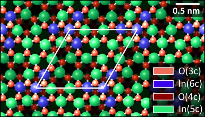
Atomic model of the In2O3(111) surface.
Different from the growth on other metal and oxide surfaces, the ordering of the 6P molecules on In2O3(111) is poor at RT, that is, the molecules do not orient themselves with respect to a high-symmetry direction of the surface. To overcome the diffusion barrier of the molecules and also to clean the surface from OH groups, a postannealing step is required, resulting in oriented molecules that are present in three equivalent orientations (because of the 3-fold symmetry of In2O3(111)), with all of the molecules featuring the same adsorption site. Thus, starting with single, randomly distributed but oriented molecules, the formation of a poorly ordered, open monolayer is observed. Upon further deposition, the open monolayer reorganizes into a well-defined, densely packed (2 × 1) monolayer. Successive growth leads to a (1 × 1) structure with respect to the In2O3(111) surface.
The molecules of the first layer 6P on In2O3(111) adsorb with the long molecular axis parallel to the substrate surface, although their adsorption and appearance in STM differ significantly from what has been observed on other substrates. Although the flat-lying 6P molecule is usually imaged as a stiff, rodlike object (occasionally with internal zigzaglike protrusions due to twisting of the phenyl rings18,19), its shape on the In2O3(111) surface resembles a slightly asymmetric “W”. Also, in the constant-height atomic force microscopy (AFM) data obtained with a CO-functionalized tip, the 6P molecule differs in appearance from what one would expect for a planar and flat molecule. However, AFM also clearly shows that five of the six phenyl rings are in a rather planar configuration and provides the adsorption site of the molecule.
Experimental Section
The STM experiments were carried out in a two-chamber UHV system equipped with an Omicron LT-STM cooled with liquid nitrogen and operated at ∼80 K. Electrochemically etched W tips were initially prepared by sputtering with Ar followed by scanning on Au(110). Voltage pulses were applied until clear atomic resolution and sharp step edges were obtained as well as a metallic signature in the scanning tunneling spectroscopy signal. The tip was treated similarly on In2O3(111) as well and was frequently refreshed on gold. Additional experiments were conducted with a commercial Omicron qPlus LT-STM at 5 K, using tuning-fork sensors20 with a separate wire for the tunneling current21 (k = 3750 N/m, fR = 47 500 Hz, Q ≈ 10 000) and a differential preamplifier.22 Electrochemically etched W tips (20 μm wire size) were glued to the tuning fork. These were cleaned in UHV by self-sputtering and field emission23 and on a Cu(100) surface by voltage pulses until a metallic behavior and frequency shift Δf between 0 and −3 Hz were attained (set point 30 pA, +1 V). For functionalization of the tip, small amounts of CO were dosed into the STM head and individual CO molecules were picked up from the In2O3 surface. Imaging 6P with a CO tip was tested on Cu(100) (see the Supporting Information and ref (35)). The data presented here are constant-current STM images probing the empty states and constant-height noncontact AFM measurements probing short-range forces. The imaging contrast due to short-range forces is composed of attractive (dark, strongly negative frequency shift) and repulsive (bright, less-negative frequency shift) interactions with the AFM tip. During the AFM measurements, a small positive bias voltage was applied and the mean tunneling current, ⟨IT⟩, was simultaneously recorded. On In2O3(111), 0.4–5 mV was applied for the metallic tips and 50–100 mV was used for CO tips.
Single crystals of indium oxide,24 cut and polished along the thermodynamically most stable (111) plane, are used here as substrates. The In2O3(111) single crystals were mounted on sample plates made of Ta. The crystal surface was cleaned by several cycles of sputtering and annealing. Sputtering was carried out in normal incidence with a focused ion gun (SPECS) scanning across the crystal surface only (1 keV Ar+, ∼1.6 μA sample current). The annealing at ∼450 °C was alternatingly performed in UHV (reducing conditions) and in oxidizing conditions, by backfilling the chamber with ∼6 × 10⁻⁷ mbar O2; this pressure was kept until the crystal was cooled to 150 °C. The final annealing was carried out in O2 to obtain a stoichiometric, relaxed bulk-terminated surface, as described in ref (7).
Sexiphenyl was deposited via thermal sublimation from powder (Tokyo Chemical Industry Co., Ltd.) using a water-cooled four-pocket evaporator (Omnivac) as well as a home-built single evaporator; in both cases, the crucible was heated indirectly by a filament. The deposition rate was monitored with a quartz crystal microbalance positioned directly in front of the sample, and the temperature of the evaporator (∼210/230 °C measured at the bottom/top of the crucible of the commercial/home-built evaporator) was set to achieve a deposition rate of ∼1–2 Å/min (density of 6P in the β-phase: 1.3 g/cm3). During deposition, the sample was kept at room temperature and afterward annealed at 200 °C for 3 min. This final annealing was used because deposition of 6P at RT results in disordered and randomly oriented molecules. Possibly, water co-evaporation contributes to the disordered character of the layer (see the Supporting Information). The postannealing allows the molecules of the first layer to diffuse, reorient, and align themselves on the surface; additionally, hydroxyl groups (originating from dissociated water from the residual gas and the evaporator) desorb from the surface. Depositing molecules directly at a substrate temperature of 200 °C leads to the same results as those of deposition at RT followed by postannealing. At this temperature, molecules of successive layers already desorb; this allows for the easy preparation of the densely packed layer by flashing off the multilayer. Higher coverages were thus annealed at 120 °C only.
Results
The growth of the first layer of sexiphenyl on In2O3(111) can be divided into two regimes in terms of the orientation and assembly of the molecules.
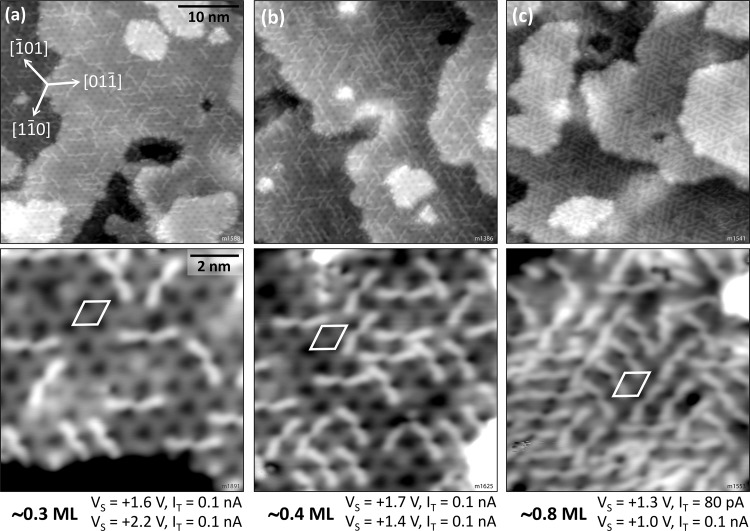
At low, sub-monolayer coverages, as shown in Figure 2a,b, single molecules are randomly distributed across the surface, with no apparent preference for step edges or defects. However, each individual molecule is clearly oriented along one of the three equivalent crystallographic ⟨11̅0⟩ directions. The adsorption site of the molecules is found to be in between the rows formed by the dark triangles of the clean In2O3(111) surface.
Figure 2.
Low-coverage regime of sexiphenyl on In2O3(111) after annealing at 200 °C; imaged with STM at 80 K. The unit cell of the In2O3 substrate is indicated in white. (a, b) Sub-monolayer coverages. (c) “Open monolayer”.
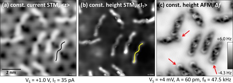
In addition to the STM measurements, the single molecules were investigated with nc-AFM. Figure 3 shows a comparison of different imaging modes; here, a metallic tip was prepared. The shape of the 6P molecules in constant-current and constant-height STM (panels (a, b)) resembles an asymmetric W, where the asymmetry in shape is identical for all molecules of the same orientation. In the constant-height frequency-shift image, panel (c), the molecules look more rodlike in general but their internal structure again shows an asymmetry along the 6P long axis. One end of the molecule, that is, the last phenyl ring, is imaged as a distinct, bright semicircle (red arrows in Figure 3c) because of repulsive interactions with the AFM tip, whereas the other end of the molecule blends into the surface. Because all of the molecules appear to be identical in STM and AFM, despite their different orientations, a single adsorption site and geometry can be deduced.
Figure 3.
Single 6P molecules imaged with STM and nc-AFM at 5 K. (a, b) Molecules adopt an asymmetric W shape, as indicated in black/yellow. (c) Constant-height nc-AFM (unknown tip) reveals an anisotropic pattern along the molecules’ long axis. One end of each 6P (red arrows) shows a clearly discerned phenyl ring.
To obtain further information about the other phenyl rings of the molecule and the exact adsorption site on the In2O3(111) surface, CO was co-dosed into the STM/AFM at 5 K and picked up by the tip, which allowed us to image the “chemical structure/backbone” of the molecules in constant-height measurements. The result is depicted in Figure 4a. Although the molecule looks very different from what one would expect for a planar and flat molecule (see 6P on Cu(100) in the Supporting Information and ref (35)), the individual phenyl rings are easily recognized. For better visibility, a high-pass filter was applied to the images in panel (b). The bright semicircle from Figure 3c, labeled “6”, is readily identified as a flat-lying phenyl ring, as are rings “2”, “3”, and “5”. Ring “1” is only faintly visible, but a gentle push with the tip during image acquisition revealed its nature as an intact phenyl ring; see Figure 5. The configuration of ring “4” remains unclear. The strong interaction between the tip and ring 4 could be a twisted configuration of the molecule. The tunneling current, ⟨IT⟩, recorded simultaneously with the frequency shift, Δf, of the constant-height AFM measurement is displayed in Figure 4c and for a slightly larger region in panel (e). Contrast enhancement reveals features of the In2O3(111) surface, that is, the dark triangles located at In(6c), which dominate the STM contrast on the uncovered surface; see also Figures 2 and 3. The superposition of the frequency shift and tunneling current signals with the (relaxed, bulk-terminated) atomic model of the bare In2O3(111) surface allows postulating a tentative adsorption geometry of a (simplified) flat-lying and planar sexiphenyl on In2O3(111); see Figure 4d. The error in position due to the alignment of Figure 4e with the lattice is about 0.1 nm.
Figure 4.
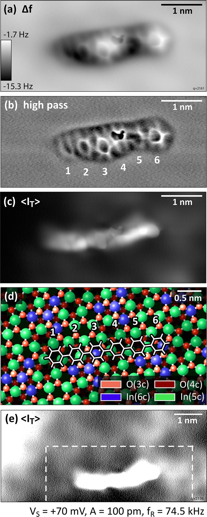
Constant-height nc-AFM images measured with a CO-terminated tip at 5 K. (a) Frequency-shift image. (b) High-pass-filtered image of (a). (c) Simultaneously acquired tunneling current signal. (d) Simplified 6P structure superimposed on the atomic model of the In2O3(111) surface. (e) Constant-height STM image showing the substrate features used as a reference for the adsorption site assignment in (d); the dark triangles in the STM images correspond to regions of the blue In(6c) atoms.
Figure 5.
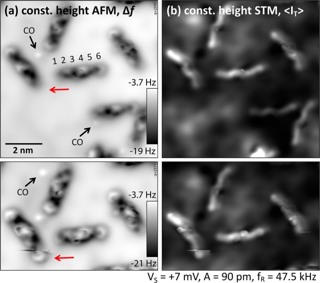
Identification of phenyl ring 1 (red arrow) by gently pushing it with the tip during image acquisition. (a) Frequency-shift signal. (b) Simultaneously recorded tunneling current. The slow scanning direction is from top to bottom. TSPM = 5 K.
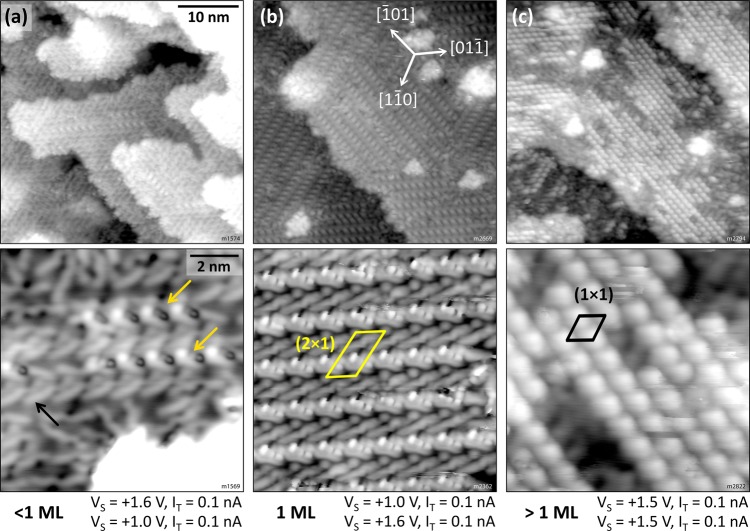
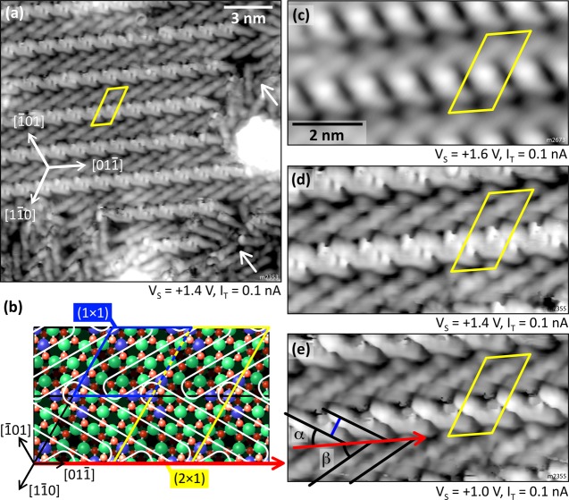
Increasing the coverage does not influence the adsorption until the whole surface is loosely covered. The molecules arrange into a so-called open monolayer where every molecule occupies the same adsorption site, whereas the whole assembly lacks long-range order because of the three possible and equivalent ⟨11̅0⟩-type orientations. Domains remain small and consist of (at most) five to six molecules; see Figure 2c. Approaching the density of one 6P per substrate unit cell, however, results in a reorientation of the molecules away from ⟨11̅0⟩ to form a new structure. The onset of this nucleation is depicted in Figure 6a, where densely packed stripes (marked by yellow arrows) are surrounded by molecules that have already re-oriented but are not yet part of the new structure (black arrow). A surface fully covered by this new structure is shown in Figure 6b. Three domains are observed, each consisting of bright, “dashed” stripes running along one of the three high-symmetry ⟨11̅0⟩ directions of the In2O3(111) surface, forming a (2 × 1) superstructure. Figure 7a shows a large domain of the new structure and its border (white arrows), where some molecules are oriented differently. The (2 × 1) unit cell is compared with the In2O3(111) cell in Figure 7b.
Figure 6.
High-coverage regime of sexiphenyl grown on In2O3(111) and after annealing at (a, b) 200 °C and (c) 120 °C. (a) Reorientation and onset of densely packed patches. (b) Densely packed (2 × 1) overlayer (defined as the first monolayer). (c) Coverage beyond the densely packed layer with a (1 × 1) periodicity. TSTM = 80 K.
Figure 7.
Densely packed (2 × 1) structure. (a) Ordered domain with loosely packed molecules at the fringes (white arrows). (b) Comparison of the In2O3(111) (1 × 1) unit cell (blue) with the 6P (2 × 1) cell (yellow). The red arrow indicates the direction of the 6P stripes, and the white ovals represent the molecules. The sites were determined from single stripes as in Figure 6a. (c) Most common imaging contrast. (d, e) Same tip termination as in (a) at different bias voltages revealing the individual molecules. (e) [011̅] surface direction is indicated by the red arrow to show the orientation of the molecules (black lines) of α = β = 30°. TSTM = 80 K.
The appearance of the (2 × 1) superstructure depends on the status of the STM tip. The most common contrast of a metallic STM tip, obtained after preparing the tip on a gold surface, is depicted in Figures 6b,top and 7c; here, the individual molecules in the darker stripes are hardly recognizable. However, poking the tip into a surface with high 6P density, and presumably picking up a molecule or fragment, always leads to similar contrasts on the (2 × 1) structure; here, the individual molecules are easily distinguished (Figure 7d,e). On close inspection, it was observed that both the bright dashed stripes and the dark spaces in between consist of densely packed 6P molecules, enclosing the angle α = β = 30° to the stripe direction (indicated in Figure 7e). This means that the molecules are symmetrically arranged around the ⟨11̅0⟩ directions of the surface, with their long axes aligned along ⟨2̅11⟩, that is, the diagonal of the In2O3 unit cell. The (2 × 1) unit cell contains two molecules, one in the dark and one in the bright stripe. This arrangement is obvious from the high-resolution images with the functionalized tip but is not so clear in the contrast obtained with metallic tips (Figure 7c). The elongated protrusions forming the bright stripes of Figure 7c also seem to enclose a different, larger, angle to the stripe direction. Our analysis (see the Supporting Information) shows that these protrusions in the contrast obtained with metallic tips are, in fact, not located exactly at the position of the molecules. This is also indicated by the (2 × 1) unit cell in panels (c–e), which is positioned with respect to the molecules of the dark stripes. In panel (c), the protrusions appear in between the molecules of the bright stripes.
The open monolayer and the (2 × 1) monolayer are the only stable structures after annealing at ∼200 °C. Depositing small amounts of additional 6P at room temperature on top of the (2 × 1) layer leads to a mostly disordered phase with some ordered patches but with an overall unstable surface during STM imaging. An ordered phase can be produced by gentle annealing at ∼120 °C. In STM, large protrusions forming a (1 × 1) pattern are observed; see Figure 6c. The apparent height of these protrusions with respect to the surrounding surface (probably the densely packed layer) is 140–170 pm. A further analysis of this structure is beyond the scope of this work.
Discussion
In this work, we have used single crystals of pure In2O3 as a model system to investigate the early stages of 6P growth on the In2O3(111) surface. The growth process is followed using scanning tunneling microscopy (STM) and noncontact atomic force microscopy (nc-AFM) at cryogenic temperatures. The use of nc-AFM, operated at a constant-height with a CO-functionalized tip, is an invaluable tool in discerning the chemical structure of organic molecules not only on insulating substrates but also, more recently, on metals and oxides.25,26 Recent overviews have been published by Jarvis27 and Jelínek.28 The sharp contrasts obtained with a CO-functionalized tip on organic molecules result from a combination of Pauli repulsion and the tilting of the flexible CO-tip due to electrostatic forces.26 Thus, the impression of the geometric structure of a molecule can be distorted by the imaging mechanism itself; other effects can also contribute, for example, dipole moments of the substrate or charge rearrangements within the molecule.29
After deposition at room temperature, single sexiphenyl molecules adsorb in a disordered manner on the In2O3(111) surface. To overcome the diffusion barrier and desorb the OH groups, a postannealing step was performed. The temperature range of 150–200 °C provides enough thermal energy to align the 6P molecules on the surface without desorbing or destroying them. Additionally, hydroxyl groups due to dissociative water adsorption are removed from the In2O3(111) surface,30 which could potentially also be a factor in the initially observed random orientation of the molecules.
Two structures that were observed in the first monolayer differ in the molecular density, orientation, adsorption sites of the molecules, and their long-range order. At lower coverage, a structure called the open monolayer here is formed with very small domains, where all of the 6P adopt the same adsorption site and are oriented along the same, equivalent low-index ⟨11̅0⟩ directions. The molecules are well-separated from each other, except for linear chains where their ends meet. Molecules of mixed orientations enclose 60°, and the end of one molecule can meet either the end or the side of the next molecule (see Figure 2b,c). Overall, apart from steric hindrance, they are not influenced by the presence of neighboring molecules, which is manifested in the lack of domain formation and long-range order. The appearance of the individual molecule in constant-current STM resembles an asymmetric W, that is, there is a significant zigzag in the apparent shape of the molecule. This differs from the way 6P usually appears in STM18,19,31 and leads to the suggestions that the molecule does not adsorb in a completely planar configuration on In2O3(111). Sexiphenyl is a structurally flexible molecule because of the single C–C bond linking the phenyl rings. This allows the molecule to bend out of plane, for example, across step edges, whereas the in-plane bending (without twisting) is limited by the sp2-hybridization of the C–C bond and steric hindrance of the hydrogen atoms. However, 6P can twist, that is, individual phenyl rings can be rotated out of plane, usually to increase the π–π overlap among neighboring molecules, which is observed in the 6P crystal structure (α-phase) and supported on surfaces both in multilayers19 and monolayers.31
Although the configuration of the molecule remains unclear from the STM images, the constant-height AFM data obtained with a CO tip deliver more details. It should be noted that the following interpretation is based purely on experimental evaluation and could serve as a useful input for future theoretical modeling. Moreover, the error in positioning is about 0.1 nm. Similar to the STM images, the appearance of 6P in constant-height AFM differs from what has been seen previously for planar and flat, rodlike conjugated molecules on metals and insulating surfaces, even if the registry of the phenyl rings with the substrate changes along the molecule.25,32,33 On In2O3(111), the 6P molecule shows phenyl rings in a rather planar geometry (the hexagons are discernable) superimposed by pronounced variations in frequency shift along the molecular long axis; see Figure 4a. The maximum (brightest contrast) is located at phenyl ring 4 (strongly interacting with the tip), followed by pairs of equal contrast, first by 3 and 6, then 2 and 5, and finally ring 1, which interacts attractively/very weakly (dark). This up-and-down configuration can be explained by the surface structure and oxygen termination of In2O3(111). The surface of In2O3(111) consists of an O(4c)–In(5c, 6c)–O(3c) trilayer, where the O(3c) atoms are the topmost atoms; see Figure 4d. The In(6c) atoms (blue in Figure 4d) are clustered in a three-pointed star and appear as dark triangles in the STM images. The surface termination is not homogeneous; it is either O(3c) or In(5c). 6P adsorbs in a position where it touches two In(6c) triangles (blue in Figure 4d). It covers only the O(3c)-terminated regions next to the In(6c) (phenyl rings 3 and 6) and In(5c) areas. In this adsorption configuration, the 6P molecule can readily avoid the O(3c)/In(5c) while interacting with as many In(5c) as possible. Thus, the variations in contrast in the AFM image, Figure 4a, are the result of electronically undistorted phenyl rings that are situated on the O(3c) regions (3 and 6) and electronically modified or geometrically twisted phenyl rings due to the strong interaction with the In(5c) underneath (2 and 5 equally, followed by 1). Although phenyl rings 4 and 1 are in a similar site, the interaction with the CO-functionalized tip is quite different. This can be, for example, due to a strong geometric twist of ring 4 or due to the fact that rings 1 and 4 differ electronically because of their different positions within the molecule. A variation in frequency shift along the molecule and particularly on ring 4 is also observed in the constant-height AFM data acquired with metallic tips; see Figures 3c and 5a. Apparently, 6P prefers undercoordinated indium but tries to avoid undercoordinated O. Within the inhomogeneous and large unit cell of In2O3(111), this is not entirely possible, and this is probably the reason why some phenyl rings twist from a planar orientation. This suggests that, by judiciously tuning the atomic structure and the distribution of undercoordinated sites, one can “steer” an organic molecule to interact with a surface in different ways, presumably with interesting consequences for the alignment of the frontier orbitals and charge injection. In summary, an essentially flat and planar adsorption geometry is proposed for single 6P molecules on In2O3(111).
Increasing the sexiphenyl coverage results in a significant reorientation of the molecules from the open monolayer into a (2 × 1) structure, once a critical coverage is reached. The molecules change from the preferred orientation of the single molecule into positions that are rotated ±30° off of these directions (i.e., from ⟨11̅0⟩ to ⟨2̅11⟩), and they adopt a densely packed structure. In STM, this 6P layer shows a prominent dark-and-bright stripe pattern, where the individual molecules are difficult to discern with a metallic tip (Figures 6b and 7c). This contrast varies slightly for different tip preparations and shows almost no bias dependence in the empty states from +1 to +1.8 V. Sometimes, the molecules within the dark stripes become more distinct (see the Supporting Information), featuring the zigzag W shape that is also characteristic of the single molecules aligned azimuthally in ⟨11̅0⟩ orientations as discussed earlier (see Figure 3). This similarity suggests that both the single molecules and those of the dark stripes are in the same, or at least a very similar, geometric configuration despite their different azimuthal orientations. The adsorption sites shown in Figure 7b were derived from intermediate coverages as in Figure 6a. According to our evaluation, the molecules of the dark and bright stripes occupy nonequivalent sites on the surface. Those of the dark stripes occupy the site where the O(3c) atoms (bound to In(5c)) are avoided most easily while maximizing the contact to In(5c) (bound to O(4c)). The 6P molecules of the bright stripes have one end directly on the O(3c)/In(6c) region, and the site is mostly O(3c)-terminated.
In the STM images, the molecules of the bright stripes appear somewhat shorter than those of the dark stripes. Moreover, the molecules within both the dark and the bright stripes are separated by ∼0.7 nm, as measured perpendicular to their long axis (distance of the parallel black lines, indicated in blue in Figure 7e). The spacing of ∼0.7 nm also corresponds to the van der Waals width of the flat 6P molecule (0.67 nm), suggesting a dense packing of the molecules if they indeed adsorb in an essentially planar fashion. Comparable values have been found for 6P on Cu(110) in the densely packed, planar, and flat monolayer (molecular spacing of 0.72 nm) and for the twisted second layer there (molecular spacing of 0.67 nm).19 An even closer arrangement occurs on O-passivated Cu(110) (2 × 1) with 0.51 nm. This compression of the 6P(203̅) layer (bulk spacing of 0.566 nm and a tilt angle of ∼33° with the 6P long axis as the rotational axis) is realized by a slightly larger tilt of ∼37°.31,34 Also, on TiO2(110), the flat-lying 6P tilts (rotation around its long axis) in the first monolayer grown at 130 °C to accommodate the substrate lattice constant of 0.65 nm in the [11̅0] direction.17
The main reason for the azimuthal reorientation of the 6P molecules into the (2 × 1) first monolayer structure is the molecule–molecule interaction that comes into play once the open monolayer cannot accommodate additional molecules because of steric hindrance. The formation of the first monolayer of 6P with molecules pointing in different directions is rather unusual. The bulk structures of 6P all feature molecules with parallel long axes; a herringbone arrangement is found only in the plane perpendicular to the long axis.10,11 Thus, the transition of 6P on In2O3(111) into the bulk phase either requires further restructuring of the (2 × 1) monolayer (probably starting with the (1 × 1) arrangement reported in this work) or takes place in the subsequent layers.
The density of the open monolayer would be 0.5 6P molecules per substrate unit cell, that is, 0.5 ML, if a single domain were to ideally cover the whole surface. Experimentally, a higher coverage is observed because of the presence of three orientations that allow the molecules to share their substrate unit cells. The transition from the open monolayer into the (2 × 1) structure happens at coverages very close to 1 ML (compare Figures 2c and 6a). The (2 × 1) unit cell contains two 6P molecules that correspond to one 6P per In2O3(111) substrate unit cell, that is, to a molecular density of 1 ML = 5.64 × 1013 cm–2. Thus, the (2 × 1) monolayer doubles the number of molecules per unit cell with respect to the ideal, single-domain open monolayer.
Conclusions
In summary, we have reported on the adsorption of single molecules and the formation of the first layer of sexiphenyl on In2O3(111), as investigated with STM. The single molecules adsorb oriented along the surface ⟨11̅0⟩ directions with their long axis parallel to the substrate surface. We find an unusual zigzaglike appearance by STM and nc-AFM, suggesting a strong interaction with In(5c) atoms of the substrate, possibly distorting the molecule. The first monolayer features a (2 × 1) structure consisting of molecules that are not uniaxially aligned but with their long axis parallel to the substrate surface and a density of one 6P molecule per substrate unit cell.
Acknowledgments
M.W. gratefully acknowledges FWF project T759-N27. Research at the Oak Ridge National Laboratory for L.A.B. was sponsored by the U.S. Department of Energy, Basic Energy Sciences, Materials Sciences and Engineering Division (DE-AC05-00OR22725). M.S. acknowledges support from FWF project F4505. U.D. acknowledges support from the European Research Council (Advanced Grant “OxideSurfaces” ERC-2011-ADG_20110209) and FWF project Wittgensteinpreis Z250.
Supporting Information Available
The Supporting Information is available free of charge on the ACS Publications website at DOI: 10.1021/acsami.8b02177.
Deposition of 6P at room temperature, 6P on Cu(100) imaged with a CO tip, and appearance of the (2 × 1) structure in STM (PDF)
The authors declare no competing financial interest.
Supplementary Material
References
- Minami T. Transparent conducting oxide semiconductors for transparent electrodes. Semicond. Sci. Technol. 2005, 20, S35–S44. 10.1088/0268-1242/20/4/004. [DOI] [Google Scholar]
- Egdell R. G.Defects at Oxide Surfaces; Jupille J.; Thornton G., Eds.; Springer International: New York, 2015; pp 351−400. [Google Scholar]
- de Wit J. H. W.; van Unen G.; Lahey M. Electron concentration and mobility in In2O3. J. Phys. Chem. Solids 1977, 38, 819–824. 10.1016/0022-3697(77)90117-2. [DOI] [Google Scholar]
- Zhang D.; Liu Z.; Li C.; Tang T.; Liu X.; Han S.; Lei B.; Zhou C. Detection of NO2 down to ppb levels using individual and multiple In2O3 nanowire devices. Nano Lett. 2004, 4, 1919–1924. 10.1021/nl0489283. [DOI] [Google Scholar]
- Gurlo A. Nanosensors: towards morphological control of gas sensing activity. SnO2, In2O3, ZnO and WO3 case studies. Nanoscale 2011, 3, 154–165. 10.1039/C0NR00560F. [DOI] [PubMed] [Google Scholar]
- Morales E. H.; He Y.; Vinnichenko M.; Delley B.; Diebold U. Surface structure of Sn-doped In2O3(111) thin films by STM. New J. Phys. 2008, 10, 125030 10.1088/1367-2630/10/12/125030. [DOI] [Google Scholar]
- Wagner M.; Seiler S.; Meyer B.; Boatner L. A.; Schmid M.; Diebold U. Reducing the In2O3(111) surface results in ordered indium adatoms. Adv. Mater. Interfaces 2014, 1, 1400289 10.1002/admi.201400289. [DOI] [Google Scholar]
- Grem G.; Leditzky G.; Ullrich B.; Leising G. Realization of a blue-light-emitting device using poly(p-phenylene). Adv. Mater. 1992, 4, 36–37. 10.1002/adma.19920040107. [DOI] [Google Scholar]
- Leising G.; Tasch S.; Meghdadi F.; Athouel L.; Froyer G.; Scherf U. Blue electroluminescence with ladder-type poly(para-phenylene) and para-hexaphenyl. Synth. Met. 1996, 81, 185–189. 10.1016/S0379-6779(96)03751-4. [DOI] [Google Scholar]
- Baker K. N.; Fratini A. V.; Resch T.; Knachel H. C.; Adams W. W.; Socci E. P.; Farmer B. L. Crystal structures, phase transitions and energy calculations of poly(p-phenylene) oligomers. Polymer 1993, 34, 1571–1587. 10.1016/0032-3861(93)90313-Y. [DOI] [Google Scholar]
- Resel R.; Koch N.; Meghdadi F.; Leising G.; Athouel L.; Froyer G.; Hofer F. A polymorph crystal structure of hexaphenyl observed in thin films. Cryst. Res. Technol. 2001, 36, 47–54. . [DOI] [Google Scholar]
- Smilgies D.-M.; Boudet N.; Yanagi H. In-plane alignment of para-sexiphenyl films grown on KCl(001). Appl. Surf. Sci. 2002, 189, 24–30. 10.1016/S0169-4332(01)01029-7. [DOI] [Google Scholar]
- Kintzel E. J. Jr.; Smilgies D.-M.; Skofronick J. G.; Safron S. A.; Van Winkle D. H. Effect of temperature on the growth of ultrathin films of p-sexiphenyl on KCl(001). J. Vac. Sci. Technol., A 2004, 22, 107–110. 10.1116/1.1631471. [DOI] [Google Scholar]
- Hlawacek G.; Teichert C.; Andreev A. Y.; Sitter H.; Berkebile S.; Koller G.; Ramsey M.; Resel R. Self-organization of para-sexiphenyl on crystalline substrates. Phys. Status Solidi A 2005, 202, 2376–2385. 10.1002/pssa.200521173. [DOI] [Google Scholar]
- Resel R.; Oehzelt M.; Lengyel O.; Haber T.; Schülle T. U.; Thierry A.; Hlawacek G.; Teichert C.; Berkebile S.; Koller G.; Ramsey M. G. The epitaxial sexiphenyl (001) monolayer on TiO2(110): A grazing incidence X-ray diffraction study. Surf. Sci. 2006, 600, 4645–4649. 10.1016/j.susc.2006.07.021. [DOI] [Google Scholar]
- Resel R. Surface induced crystallographic order in sexiphenyl thin films. J. Phys.: Condens. Matter 2008, 20, 184009 10.1088/0953-8984/20/18/184009. [DOI] [Google Scholar]
- Sun L.; Berkebile S.; Weidlinger G.; Koller G.; Hohage M.; Netzer F. P.; Ramey M. G.; Zeppenfeld P. Revealing the buried interface: para-sexiphenyl thin films grown on TiO2(110). Phys. Chem. Chem. Phys. 2010, 12, 3141–3144. 10.1039/b922285e. [DOI] [PubMed] [Google Scholar]
- Koller G.; Surnev S.; Ramsey M. G.; Netzer F. P. Sexiphenyl on a Ni(110)(2 × 1)-O surface: A single-molecule STM study. Surf. Sci. 2004, 559, L187–L193. 10.1016/j.susc.2004.04.019. [DOI] [Google Scholar]
- Wagner M.; Berkebile S.; Netzer F. P.; Ramsey M. G. Revealing the buried metal–organic interface: Restructuring of the first layer by van der Waals forces. ACS Nano 2015, 9, 12070–12078. 10.1021/acsnano.5b05013. [DOI] [PubMed] [Google Scholar]
- Giessibl F. J.Sensor for Noncontact Profiling of a Surface. U.S. Patent 20120131704 A1, 2012.
- Majzik Z.; Setvín M.; Bettac A.; Feltz A.; Cháb V.; Jelínek P. Simultaneous current, force and dissipation measurements on the Si(111) 7 × 7 surface with an optimized qPlus AFM/STM technique. Beilstein J. Nanotechnol. 2012, 3, 249–259. 10.3762/bjnano.3.28. [DOI] [PMC free article] [PubMed] [Google Scholar]
- Huber F.; Giessibl F. Low noise current preamplifier for qPlus sensor deflection signal detection in atomic force microscopy at room and low temperatures. Rev. Sci. Instrum. 2017, 88, 073702 10.1063/1.4993737. [DOI] [PubMed] [Google Scholar]
- Setvín M.; Javorský J.; Turčinková D.; Matolínová I.; Sobotík P.; Kocán P.; Ošt’ádal I. Ultrasharp tungsten tips–characterization and nondestructive cleaning. Ultramicroscopy 2012, 113, 152–157. 10.1016/j.ultramic.2011.10.005. [DOI] [Google Scholar]
- Wagner M.; Setvín M.; Schmid M.; Diebold U.. Sexiphenyl on Cu(100): nc-AFM tip functionalization and identification. Surf. Sci. 2018, in press. 10.1016/j.susc.2018.03.004 [DOI] [Google Scholar]
- Hagleitner D. R.; Menhart M.; Jacobson P.; Blomberg S.; Schulte K.; Lundgren E.; Kubicek M.; Fleig J.; Kubel F.; Puls C.; Limbeck A.; Hutter H.; Boatner L. A.; Schmid M.; Diebold U. Bulk and surface characterization of In2O3(001) single crystals. Phys. Rev. B 2012, 85, 115441 10.1103/PhysRevB.85.115441. [DOI] [Google Scholar]
- Gross L.; Mohn F.; Moll N.; Liljeroth P.; Meyer G. The chemical structure of a molecule resolved by atomic force microscopy. Science 2009, 325, 1110. 10.1126/science.1176210. [DOI] [PubMed] [Google Scholar]
- Hapala P.; Kichin G.; Wagner C.; Tautz F. S.; Temirov R.; Jelinek P. Mechanism of high-resolution STM/AFM imaging with functionalized tips. Phys. Rev. B 2014, 90, 085421 10.1103/PhysRevB.90.085421. [DOI] [PubMed] [Google Scholar]
- Jarvis S. P. Resolving intra- and inter-molecular structure with non-contact atomic force microscopy. Int. J. Mol. Sci. 2015, 16, 19936–19959. 10.3390/ijms160819936. [DOI] [PMC free article] [PubMed] [Google Scholar]
- Jelínek P. High resolution SPM imaging of organic molecules with functionalized tips. J. Phys.: Condens. Matter 2017, 29, 343002 10.1088/1361-648X/aa76c7. [DOI] [PubMed] [Google Scholar]
- Meier T.; Pawlak R.; Kawai S.; Geng Y.; Liu X.; Decurtins S.; Hapala P.; Baratoff A.; Liu S.-X.; Jelínel P.; Meyer E.; Glatzel T. Donor-acceptor properties of a single-molecule altered by on-surface complex formation. ACS Nano 2017, 11, 8413–8420. 10.1021/acsnano.7b03954. [DOI] [PubMed] [Google Scholar]
- Wagner M.; Lackner P.; Steffen S.; Brunsch A.; Bliem R.; Gerhold S.; Wang Z.; Osiecki J.; Schulte K.; Boatner L. A.; Schmid M.; Meyer B.; Diebold U. Resolving the structure of a well-ordered hydroxyl overlayer on In2O3(111): Nanomanipulation and theory. ACS Nano 2017, 11, 11531–11541. 10.1021/acsnano.7b06387. [DOI] [PMC free article] [PubMed] [Google Scholar]
- Oehzelt M.; Grill L.; Berkebile S.; Koller G.; Netzer F. P.; Ramsey M. G. The molecular orientation of para-Sexiphenyl on Cu(110) p(2 × 1)O. ChemPhysChem 2007, 8, 1707–1712. 10.1002/cphc.200700357. [DOI] [PubMed] [Google Scholar]
- de Oteyza D. G.; Gorman P.; Chen Y.-C.; Wickenburg S.; Riss A.; Mowbray D. J.; Etkin G.; Pedramrazi Z.; Tsai H.-Z.; Rubio A.; Crommie M. F.; Fischer F. R. Direct imaging of covalent bond structure in single-molecule chemical reactions. Science 2013, 340, 1434–1437. 10.1126/science.1238187. [DOI] [PubMed] [Google Scholar]
- Schuler B.; Zhang Y.; Collazos S.; Fatayer S.; Meyer G.; Pérez D.; Guitián E.; Harper M. R.; Kushnerick J. D.; Peña D.; Gross L. Characterizing aliphatic moieties in hydrocarbons with atomic force microscopy. Chem. Sci. 2017, 8, 2315–2320. 10.1039/C6SC04698C. [DOI] [PMC free article] [PubMed] [Google Scholar]
- Novák J.; Oehzelt M.; Berkebile S.; Koini M.; Ules T.; Koller G.; Haber T.; Resel R.; Ramsey M. G. Crystal growth of para-sexiphenyl on clean and oxygen reconstructed Cu(110) surfaces. Phys. Chem. Chem. Phys. 2011, 13, 14675–14684. 10.1039/c1cp20413k. [DOI] [PubMed] [Google Scholar]
Associated Data
This section collects any data citations, data availability statements, or supplementary materials included in this article.


