Abstract
We propose and numerically demonstrate an ultra-broadband graphene-based metamaterial absorber, which consists of multi-layer graphene/dielectric on the SiO2 layer supported by a metal substrate. The simulated result shows that the proposed absorber can achieve a near-perfect absorption above 90% with a bandwidth of 4.8 Thz. Owing to the flexible tunability of graphene sheet, the state of the absorber can be switched from on (absorption > 90%) to off (reflection > 90%) in the frequencies range of 3–7.8 Thz by controlling the Fermi energy of graphene. Moreover, the absorber is insensitive to the incident angles. The broadband absorption can be maintained over 90% up to 50°. Importantly, the design is scalable to develop broader tunable terahertz absorbers by adding more graphene layers which may have wide applications in imaging, sensors, photodetectors, and modulators.
Keywords: Thz absorption, Surface plasmons, Metamaterials, Tunable Thz devices
Background
In recent years, the terahertz band has become one of the most interesting platform because of the huge application in spectroscopy, medical imaging, modulators, security, and communication [1–3]. The terahertz absorber is an important branch, which can find practical applications in the above fields [4–6]. However, the narrow bandwidth, low absorption efficiency, and non-adjustable absorption performance of the absorbers limit their applications in practice greatly. In order to better expand the application of terahertz absorber, more new devices and materials are urgently required. Graphene, as a two-dimensional material with the honeycomb lattice structure, has become one of the most promising materials due to its tunability of conductivity controlled by electric field, magnetic field, gate voltage, and chemical doping [7–14]. Especially, graphene can support surface plasmons in the terahertz ranges. Compared with the traditional surface plasmon material, graphene surface plasmons have the advantage of low losses, flexible tunability and so on [15–19].
Owing to the superiority of graphene materials in terahertz absorbers, there are some graphene absorbers that have been proposed and demonstrated [20–34]. Theoretical analysis confirms that a single layer of graphene is optically transparent and it has an absorption of 2.3% [35–37]. To enhance the confinement of the electromagnetic energy, periodical patterned graphene structures have been designed such as net-shaped [20–22], anti-dots [23], and cross-shaped [32]. However, these absorbers are deeply dependent on complex structured graphene which result in fabrication difficulty. Moreover, the band available for operation is very narrow, and most of the works reported do not have bandwidth of more than 1.5 Thz [20–28]. In order to broaden the bandwidth, several multilayer graphene structures have been proposed. However, the reported multilayer structures are also dependent on very complex structure of the graphene, and the operation bandwidths are not long enough [32–34]. In addition, Zhao et al. designed a switchable terahertz absorber for the application of amplitude modulator [25]. By controlling the chemical potential of graphene from 0 to 0.3 eV, the state of the designed structure can be switched from absorption (> 90%) to reflection (> 82%) in the frequencies range of 0.53–1.05 Thz. But the switching intensity is not high enough, and the modulation bandwidth is very narrow, which limit its further application in practice.
In this paper, we present a tunable graphene-based terahertz absorber composed of multilayer graphene which can achieve an ultra-broadband absorption over 90% in the frequencies range of 3–7.8 Thz. The average absorptivity of the absorber is higher than 96.7%. Besides, the proposed absorber has higher switching intensity, the absorption amplitude can be tuned from near-perfect absorption (> 90%) to high reflection (> 90%) by changing the Fermi energy of graphene layer in the whole bandwidth of 4.8 Thz. When the Fermi energy of graphene is 0 eV, the proposed structure will be a near-perfect reflector with a reflection more than 97% in the high frequency band (about 5.5 Thz later). In addition, the absorber is independent to the incident angles with the absorption more than 90% up to 50°. To our best knowledge, we first propose the two-dimensional multi-layer graphene/dielectric structure to realize an ultra-broadband absorption. The proposed absorber is simple which do not depend on complex patterned graphene, and the design provides great convenience for the fabrication of multilayer graphene structures [38, 39]. Importantly, the design is scalable to develop broader tunable terahertz absorbers by adding more graphene layers, which may have wide application in terahertz optoelectronic devices.
Methods
The diagram of the proposed structure is shown in Fig. 1, which consists of multi-layer graphene embedded into the dielectric on the SiO2 layer and a thick metallic reflecting plate on the bottom. As shown in Fig. 1, on the top, graphene with different width (W) is embedded in the dielectric at a certain gap t2 (t2 = 2 μm). The width W of each graphene is 5, 5, 27, 4, 4, 2, 21, 21, and 26 μm, respectively (from top to bottom). Each layer is symmetrical about the z-axis. The distance t1 between the bottom of the graphene layer and the SiO2 layer is 2 μm. The thickness of the dielectric is H1. The middle layer is SiO2 with a thickness of H2. The bottom is a metallic film with a thickness of D. The period of the unit is P. These initial values of the structure parameters are set to H1 = 21 μm, H2 = 7 μm, D = 0.5 μm, P = 32 μm. The bottom metallic material is gold, and its permittivity can be properly represented by the Drude model in terahertz range as follows:
| 1 |
where the value of constant permittivity ε∞, plasma frequency ωp, and collision frequency γ are set to 1, 1.38 × 10¹⁶ rad/s, and 1.23 × 10¹³ s− 1, respectively. The permittivity of the dielectric material and SiO2 material are set to 3 and 4, respectively.
Fig. 1.

a Schematic diagram of the graphene-based broadband absorber. b Cross section of the absorber with the parameters used for calculation. c The schematic of the external bias circuit. The branches of the voltage (V1~V9) are connected to diferent graphene layers, respectively
In the simulation, graphene is treated as an ultra-thin film embedded in the dielectric. The complex graphene surface conductivity dominated by interband and intraband contributions can be calculated by using the Kubo formula [40]:
| 2 |
where is the Fermi-Dirac distribution, w is the radian frequency, ε is the energy, kB is the Boltzmann’s constant, τ is the carrier relaxation time, T is the temperature (T = 300 K in our paper), ℏ is the reduced Plank’s constant, and Ef is Fermi energy. The Kubo formula (2) indicates that the complex graphene surface conductivity can be adjusted by Fermi energy Ef. The graphene Fermi energy of each layer can be individually controlled by the biased voltage, the relation between Ef and biased voltage can be written as [41, 42]:
| 3 |
where vF = 0.9 × 10⁶m/s is the Femi velocity, V0 is the voltage offset [41], , a0 is the capacitive model of the structure, where ε0 is the permittivity in vacuum. εd is the permittivity of dielectric, d is the height of dielectric, and e is the charge of an electron. Vn(V1~V9), that is, the voltage applied to the graphene can be obtained from the additional circuit of Fig. 1c. According to Formula (2) and (3), graphene’s surface conductivity can be controlled by the applied voltage. Then, based on the Ampere’s law in stationary regime and Ohm’s law, the permittivity of graphene can be obtained as [43]:
| 4 |
In which tg is the thickness of the graphene, ε0 is the permittivity of vacuum, and σg is the surface conductivity of the graphene. According to Formula (4), the permittivity of graphene can be obtained by the surface conductivity, which can also be obtained by the applied voltage. Therefore, Formula (2–4) indicate that the electromagnetic properties of graphene can be dynamically controlled by the applied voltage, leading to that the absorption characteristics of the structure can also be dynamically controlled.
To investigate the absorption performance of the designed structure, we implement the numerical simulations using two-dimensional FDTD. In our simulation, we set the structure to a periodic boundary condition in the x direction. A beam of terahertz plane wave is incident to the model normally along the z direction with its electric field E along x direction. The Bloch boundary condition is applied to the oblique incidence in the periodic structure. We use 1-R-T to calculate the absorption of the model, where R and T represent reflectivity and transmissivity, respectively. Since the thickness of the metal is much greater than the skin depth of incident light in the metal, the transmissivity T is zero. Thus, we simplify the calculation formula for 1-R.
Results and Discussion
Firstly, we tune the voltage of each graphene layer to achieve perfect absorption (from top to bottom, we fine adjust the Fermi energy Ef of the each graphene layer to 0.9, 0.9, 1.1, 0.8, 0.8, 1.1, 1.1, 0.9, and 0.8 eV). As shown in Fig. 2, from 3 to 7.8 Thz, the proposed structure has a broadband absorption above 90% within a bandwidth of 4.8 Thz. The FWHM of the absorber is 5.4 Thz. The bandwidth is about = 88.8% of central frequency (here, BW is the bandwidth and f0 is central frequency). We also calculate the average absorptivity of the absorber, which is as high as 96.7%. On the other hand, with the Ef = 0 eV, the proposed structure will be a near-ideal reflector with reflection more than 90% over the whole operation bandwidth, and in the high frequency band (about 5.5 Thz later), the reflection even more than 97%. Of course, we can also tune the voltage of each graphene layer to get the desired amplitude which may have potential applications in some areas.
Fig. 2.
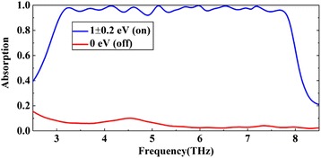
The calculated absorption spectra of the proposed absorber, where the blue line represents the absorption with high voltage and the red line indicates the absorption with no voltage applied
In order to explain the near-perfect absorption in an ultra-broad bandwidth, firstly, we discuss the situation of a single graphene layer. As shown in Fig. 3a, we design the structure with only one single graphene layer embedded into the dielectric. Based on graphene surface plasmons, we investigate the effect of graphene-related parameters on the absorption performance of absorber, including the Fermi energy Ef, the width W, and the position t of graphene.
Fig. 3.
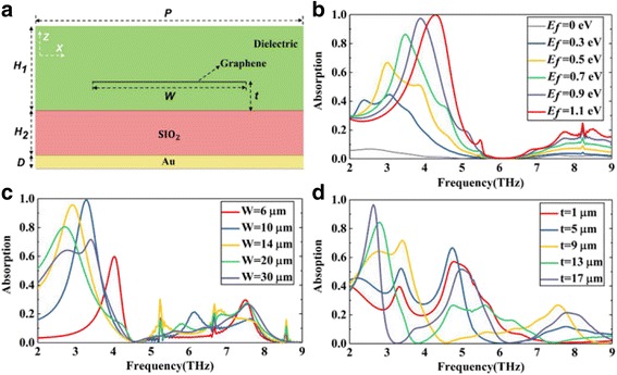
a Schematic diagram of a single-layer graphene structure. b–d The absorption of the structure width different Fermi energy Ef, width W, and position t of the graphene sheet, respectively
Figure 3b shows the influence of graphene Fermi energy Ef on the absorption spectrum with fixed W and t. As the increase of Ef, the graphene surface plasmon resonance becomes stronger, the absorption of the structure is higher correspondingly. The absorption peak even more than 99% at 4.3 Thz with the Ef = 1.1 eV. And the resonance absorption peak moves to a higher frequency, blue shift. Similarly, Fig. 3c, d shows the absorption spectrum of the structure with different W or t with unchanged Ef . By varying the W or t of the graphene layer, the amplitude and frequency of the resonance peak are changed respectively. This phenomenon can be explained by the circuit theory [28]. In this theory, graphene is described as a shunt admittance, then the equivalent circuit of the structure can be modeled with transmission lines and graphene admittance. According to previous work [28], the graphene admittance can be changed by the width W and the Fermi energy Ef of the graphene. In addition, the admittance of the transmission lines corresponding to dielectric are related to the thickness of the dielectric. In our structure, the dielectric is separated by graphene layer. Thus, the position t of the graphene layer also affects the input admittance of the structure.
As we discussed above, due to the influence of graphene-related parameters on the input admittance of the structure, the resonance absorption peaks of the model are also influenced. If the input admittance of the structure matches to the free-space admittance, the near-perfect absorption at a certain frequency is achieved.
Then, in order to achieve broadband absorption, we need to allow the resonance absorption peaks which achieve the admittance matching close to each other. As the absorption peaks are close enough to merge, a broadband absorption is obtained. Therefore, we add graphene layers to get more resonance absorption peaks. And at the same time, we adjust the parameters that affect the resonance peak, including Ef, W, and t to implement admittance matching. We first add two layers of graphene. As shown in Fig. 4a, three layers of graphene with different width W are embedded in the dielectric. There is a certain interval t between different layers of graphene or the bottom graphene from the dielectric. We adjust the graphene-related parameters to the appropriate values, where we set t = 2 μm, Ef = 0.9 eV, and W = 26, 21, and 20 μm, respectively (from bottom to top).
Fig. 4.

a Schematic diagram of a three-layer graphene structure. b The calculated absorption spectra of three-layer graphene structure
As shown in Fig. 4b, the structure has a near-perfect absorption bandwidth of 1.3 Thz with a center frequency of 5.25 Thz. Three resonance peaks at 4.7, 5.2, and 5.7 Thz are obtained corresponding to the absorption amplitude of 99.9, 99.9, and 99.1%, respectively. In order to achieve an ultra-broadband absorption, similar to the three-layer graphene structure, we add more graphene layers and adjust the graphene parameters of each graphene layer to the appropriate values. We assume that the structural parameters are fixed and the production is completed; we can dynamically adjust the Fermi energy of graphene to achieve broadband absorption. Based on the principle of impedance matching and the research experience of three-layer graphene structure, we first assume that the Fermi level of each layer of graphene is 1 eV. As shown in Fig. 5 (a), the absorption of most bands is over 90% except for the band “1” and “2”. Figure 5 (a–e) shows the gradual adjustment process for perfect absorption of the “1” and “2” bands. According to Fig. 6e, f, the absorption of the last band “1” is dominated by the fourth layer (from bottom to top), so we adjust the Fermi energy of this layer individually. As shown in Fig. 7, when the Fermi energy is 0.8 eV, the absorption performance is best. This is because the Fermi energy affects the impedance of graphene, and then affects the input impedance of the whole structure. The larger or smaller Fermi energy of graphene will lead to impedance mismatch. From a to b, we have improved the absorption performance of the “1” band (in the band before “1”, curves a and b are approximately overlapping). Similarly, we find that the energy distribution in the “2” band is mainly concentrated on the 5th, 8th, and 9th layers. We first set the Fermi energy of 8th and 9th layers of graphene to 0.9 and 0.8 eV, respectively. As shown in Fig. 5, from b to c, in addition to dip “3” and “4”, the absorption of the remaining band in “2” is over 90%. Then, according to Fig. 6c, dip “3” is mainly influenced by the 5th layer of graphene, we set the Fermi energy to 0.8 eV. From c to d, the absorption performance at dip “3” has also been improved. However, according to Fig. 6d, dip “4” is affected by all layers of graphene. Therefore, we adjust the Fermi energy of the remaining graphene layer to the appropriate value. From d to e, the near-perfect broadband absorption is achieved. Compared with the three-layer graphene structure shown in Fig. 4, more resonance absorption peaks are obtained, absorption peaks of different frequencies are close to each other and superimposed to form an ultra-broadband absorption above 90% with a bandwidth of 4.8 Thz.
Fig. 5.
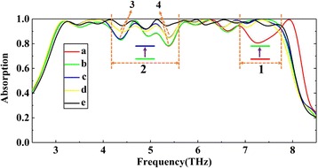
(a)–(e) show the gradual adjustment process for perfect absorption. Fermi energy of each layer of graphene (from bottom to top) are set as (a) [1] eV, (b) [1, 1, 1, 0.8, 1, 1, 1, 1, 1] eV, (c) [1, 1, 1, 0.8, 1, 1, 1, 0.9, 0.8] eV, (d) [1, 1, 1, 0.8, 0.8, 1, 1, 0.9, 0.8] eV, and (e) [0.9, 0.9, 1.1, 0.8, 0.8, 1.1, 1.1, 0.9, 0.8] eV
Fig. 6.

a–f The distributions of the electric field amplitude (|E|) of the proposed absorber at different frequencies
Fig. 7.
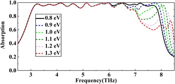
Absorption spectra with different Ef of the fourth layer of graphene and with unchanged Ef of other layers of graphene
To understand the physical mechanism behind the ultra-broadband near-perfect absorption, we also give a detailed calculation and analysis about the electric field amplitude (|E|) distributions of the proposed structure at different operating frequency. As shown in Fig. 6, the energy of the light field is confined between the different layers of graphene and dielectric, leading to a strong absorption. The characteristics of the electric field distributions are consistent with the absorption spectrum shown in Fig. 2. At a certain frequency, for example, Fig. 6b shows the electric field confinement is mainly due to the strong coupling of graphene and dielectric owing to the excitation of localized surface plasmon (LSP), Fig. 6d shows the graphene surface plasmas play a major role in the electric field confinement. The excitation of localized surface plasmon (LSP) and graphene surface plasmas contribute to the strong absorption together. Figure 6a, b, d and Fig. 6c, e, f show that the strong coupling between graphene and dielectric at a certain frequency may be caused by multi-layer graphene or monolayer graphene, respectively. The stacking of high absorption at different frequencies creates a broadband absorption under the action of all layers of graphene.
In order to better illustrate the stacking effect, for example, according to Fig. 6e, f, the absorption of the last band (about 6.5 Thz later) is mainly dominated by the fourth layer of graphene (from bottom to top). So, we tune the voltage of this layer of graphene. As shown in Fig. 7, with the increase of the Fermi energy of the fourth layer of graphene, the absorption amplitude of the band after about 6.5 Thz gradually increases, but there is almost no change in the band before 6.5 Thz. Similarly, we can also independently adjust a certain band mainly affected by other layers of graphene. All bands which can be adjusted independently for high absorption are superimposed to form a broadband absorption eventually. As with the analysis of Fig. 7, the phenomenon of independent adjustment further illustrates that the stacking effect of all layers of graphene achieves a near-perfect broadband absorption.
As discussed above, the strong coupling between graphene and the dielectric plays a major role in broadband absorption. In the practical applications, we hope that the broadband absorption is insensitive to the incident angles. As shown in Fig. 8, we investigate the effect of the incident angles on the absorber. From Fig. 8, we can find that the proposed absorber is insensitive to incident angles. Although the incident angle has changed to 30°, the absorption performance of the structure is almost unaffected. As the incident angle increases to 50°, although the absorption efficiency is reduced, the absorber still maintains a high absorption more than 90% in the whole operating bandwidth. Therefore, the absorber can work well with high absorption efficiency over a large range of incident angle.
Fig. 8.
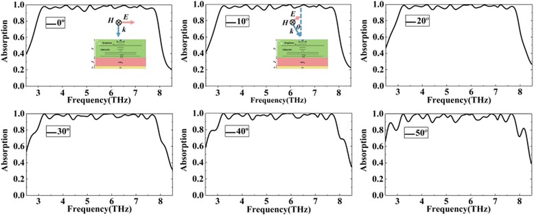
The calculated absorption spectra of the absorber with different incident angles
Finally, considering the difficulties of multi-layer structure in fabrication, we discuss the effect of the relevant structure parameters on the absorber performance. Figure 9a, b show the absorption spectra of the proposed absorber with different thickness of the dielectric layer H1 and with different thickness of the SiO2 layer H2, respectively. As shown in Fig. 9a, the most suitable height of the dielectric H1 is 21 μm. On this basis, H1 increase or decrease 0.5 μm, the performance of the absorber almost has no change. Even if H1 changes by 1 μm, the absorber still maintains an absorption above 90% in most bands except the band around 7 Thz. As shown in Fig. 9b, compared with H1, the absorber is more sensitive to the height of the SiO2H2. Even in this case, in addition to the band around 6 and 7.1 Thz, the absorber also maintains a good performance in the most bands. As discussed above, we can find that although the thickness of the dielectric layer and the SiO2 layer are changed even at the micron scale, the absorber still maintains a good absorption performance in most wavelengths which will greatly improve the robustness of the absorber in the fabrication.
Fig. 9.

The simulated absorption spectra of the proposed absorber with different thickness of the dielectric layer and with different thickness of the SiO2 layer corresponding to a and b
Conclusions
In this paper, we propose an ultra-broadband, tunable graphene-based terahertz absorber consisting of multilayers of graphene/dielectric. The proposed absorber can achieve a broadband absorption over 90% with a bandwidth of 4.8 Thz through altering the Fermi energy Ef of different graphene layers. With the Ef = 0 eV, the proposed design will be a near-ideal reflector with reflection more than 90% within the whole operation bandwidth of 3–7.8 Thz. The ultra-broadband absorption is ascribed to the stacking effect of strong resonance absorption at different frequencies excited by localized surface plasmon (LSP) and graphene surface plasmons. In addition, the proposed absorber is insensitive to the incidence angles, and we also find that the thickness of the dielectric layer and the SiO2 layer has little effect on the absorption performance, which is more beneficial to practical applications. Moreover, the proposed absorber is simple which do not depend on complex structured graphene and the bandwidth may be widened by adding more graphene layers. This tunable broadband absorber may have great potential applications in photodetectors, imaging, and modulators.
Acknowledgements
We acknowledge the support from the Ministry of Science and Technology of China (Grant No. 2016YFA0301300) and National Nature Science Foundation of China (Grant Nos. 61275201 and 61372037).
Availability of Data and Materials
The datasets generated during and/or analyzed during the current study are available from the corresponding authors on reasonable request.
Abbreviations
- FDTD
Finite-difference time-domain
- LSP
Localized surface plasmon
Authors’ Contributions
ZX and DW carried out the simulation and analysis. YL and LY supervised the writing of the manuscript. CL created the figures. HY and ZY supervised the whole work. All the authors have read and approved the final manuscript.
Competing Interests
The authors declare that they have no competing interests.
Publisher’s Note
Springer Nature remains neutral with regard to jurisdictional claims in published maps and institutional affiliations.
Contributor Information
Zenghui Xu, Email: xuechoandxi@hotmail.com.
Dong Wu, Email: dongwd@hotmail.com.
Yumin Liu, Email: microliuyumin@hotmail.com.
Chang Liu, Email: changgebupt@foxmail.com.
Zhongyuan Yu, Email: yuzhongyuan30@hotmail.com.
Li Yu, Email: yulibupt@163.com.
Han Ye, Email: dabombyh@aliyun.com.
References
- 1.Federici J, Moeller L. Review of terahertz and subterahertz wireless communications. J Appl Phys. 2010;107(11):6–323. doi: 10.1063/1.3386413. [DOI] [Google Scholar]
- 2.Jepsen PU, Cooke DG, Koch M. Terahertz spectroscopy and imaging—modern techniques and applications. Laser Photonics Rev. 2012;6(3):418–418. doi: 10.1002/lpor.201200505. [DOI] [Google Scholar]
- 3.Li Z, Ma Y, Huang R, et al. Manipulating the plasmon-induced transparency in terahertz metamaterials. Opt Express. 2013;24(21):8912–8919. doi: 10.1364/OE.19.008912. [DOI] [PubMed] [Google Scholar]
- 4.Liu M, Yin X, Ulin-Avila E, et al. A graphene-based broadband optical modulator. Nature. 2011;474(7349):64. doi: 10.1038/nature10067. [DOI] [PubMed] [Google Scholar]
- 5.Tao H, Landy NI, Bingham CM, et al. A metamaterial absorber for the terahertz regime: design, fabrication and characterization. Opt Express. 2008;16(10):7181–7188. doi: 10.1364/OE.16.007181. [DOI] [PubMed] [Google Scholar]
- 6.Landy NI, Bingham CM, Tyler T et al (2008) Design, theory, and measurement of a polarization insensitive absorber for terahertz imaging. Phys Rev B Condens Matter Mater Phys:79(12)
- 7.Geim AK, Novoselov KS. The rise of graphene. Nat Mater. 2007;6(3):183–191. doi: 10.1038/nmat1849. [DOI] [PubMed] [Google Scholar]
- 8.Geim AK. Graphene: status and prospects. Science. 2009;324(5934):1530–1534. doi: 10.1126/science.1158877. [DOI] [PubMed] [Google Scholar]
- 9.Li Q, Tian Z, Zhang X, et al. Active graphene–silicon hybrid diode for terahertz waves. Nat Commun. 2015;6:7082. doi: 10.1038/ncomms8082. [DOI] [PMC free article] [PubMed] [Google Scholar]
- 10.Fallahi A, Perruisseau-Carrier J. Design of tunable biperiodic graphene metasurfaces. PhysRevB. 2012;86(19):4608–4619. [Google Scholar]
- 11.He X, Zhao ZY, Shi W. Graphene-supported tunable near-IR metamaterials. Opt Lett. 2015;40(2):178–181. doi: 10.1364/OL.40.000178. [DOI] [PubMed] [Google Scholar]
- 12.Zhu ZH, Guo CC, Liu K, et al. Electrically tunable polarizer based on anisotropic absorption of graphene ribbons. Applied Physics A. 2014;114(4):1017–1021. doi: 10.1007/s00339-014-8269-7. [DOI] [Google Scholar]
- 13.Bolotin KI, Sikes KJ, Jiang Z, et al. Ultrahigh electron mobility in suspended graphene. Solid State Commun. 2008;146(9):351–355. doi: 10.1016/j.ssc.2008.02.024. [DOI] [Google Scholar]
- 14.Novoselov KS, Fal’Ko VI, Colombo L, et al. A roadmap for graphene. Nature. 2012;490(7419):192. doi: 10.1038/nature11458. [DOI] [PubMed] [Google Scholar]
- 15.Chen J, Badioli M, Alonsogonzález P, et al. Optical nano-imaging of gate-tunable graphene plasmons. Nature. 2012;487(7405):77. doi: 10.1038/nature11254. [DOI] [PubMed] [Google Scholar]
- 16.Grigorenko AN, Polini M, Novoselov KS. Graphene plasmonics. Nat Photonics. 2012;6(11):749–758. doi: 10.1038/nphoton.2012.262. [DOI] [Google Scholar]
- 17.Minovkoppensich FHL, Chang DE, Thongrattanasiri S, et al. Graphene Plasmonics: a platform for strong light-matter interactions. Nano Lett. 2011;11(8):3370. doi: 10.1021/nl201771h. [DOI] [PubMed] [Google Scholar]
- 18.Jablan M, Buljan H, Soljačić M (2009) Plasmonics in graphene at infrared frequencies[J]. Phys Rev B 80(24):308-10.
- 19.Sanshui X, Xiaolong, et al (2016) Graphene-plasmon polaritons: From fundamental properties to potential applications[J]. 物理学前沿(英文版) 11(2):117801.
- 20.Zhu W, Rukhlenko ID, Si LM, et al. Graphene-enabled tunability of optical fishnet metamaterial. Appl Phys Lett. 2013;102(12):77. [Google Scholar]
- 21.Zhang J, Guo C, Liu K, et al. Coherent perfect absorption and transparency in a nanostructured graphene film. Opt Express. 2014;22(10):12524–12532. doi: 10.1364/OE.22.012524. [DOI] [PubMed] [Google Scholar]
- 22.Cai G, Zhu J, Ye L, et al. Broadband absorber with periodically sinusoidally-patterned graphene layer in terahertz range. Opt Express. 2017;25(10):11223. doi: 10.1364/OE.25.011223. [DOI] [PubMed] [Google Scholar]
- 23.Nikitin AY, Guinea F, Martin-Moreno L. Resonant plasmonic effects in periodic graphene antidot arrays. Appl Phys Lett. 2012;101(15):109. doi: 10.1063/1.4760230. [DOI] [Google Scholar]
- 24.Zhang Y, Feng Y, Zhu B, et al. Graphene based tunable metamaterial absorber and polarization modulation in terahertz frequency. Opt Express. 2014;22(19):22743–22752. doi: 10.1364/OE.22.022743. [DOI] [PubMed] [Google Scholar]
- 25.Zhao YT, Wu B, Huang BJ, et al. Switchable broadband terahertz absorber/reflector enabled by hybrid graphene-gold metasurface. Opt Express. 2017;25(7):7161. doi: 10.1364/OE.25.007161. [DOI] [PubMed] [Google Scholar]
- 26.Zhihong Z, Chucai G, Jianfa Z, et al. Broadband single-layered graphene absorber using periodic arrays of graphene ribbons with gradient width. Applphysexpress. 2015;8(1):015102. [Google Scholar]
- 27.Khavasi A. Design of ultra-broadband graphene absorber using circuit theory. J Opt Soc Am B. 2015;32(9):1941. doi: 10.1364/JOSAB.32.001941. [DOI] [Google Scholar]
- 28.Arik K, Abdollahramezani S, Khavasi A. Polarization insensitive and broadband terahertz absorber using graphene disks. Plasmonics. 2017;12(2):1–6. doi: 10.1007/s11468-016-0276-4. [DOI] [Google Scholar]
- 29.Yu P, et al. Dual-band absorber for multispectral plasmon-enhanced infrared photodetection. J Phys D Appl Phys. 2016;49(36):365101. doi: 10.1088/0022-3727/49/36/365101. [DOI] [Google Scholar]
- 30.Huo D, et al. Broadband perfect absorber with monolayer MoS 2 and hexagonal titanium nitride nano-disk array. Nanoscale Res Lett. 2017;12(1):465. doi: 10.1186/s11671-017-2232-4. [DOI] [PMC free article] [PubMed] [Google Scholar]
- 31.Xiao B, et al. Absorption enhancement in graphene with an efficient resonator. Opt Quant Electron. 2017;49(5):177. doi: 10.1007/s11082-017-1013-8. [DOI] [Google Scholar]
- 32.Xiao B, Gu M, Xiao S. Broadband, wide-angle and tunable terahertz absorber based on cross-shaped graphene arrays. Appl Opt. 2017;56(19):5458. doi: 10.1364/AO.56.005458. [DOI] [PubMed] [Google Scholar]
- 33.Fardoost A, Vanani FG, Amirhosseini A, et al. Design of a multilayer graphene-based ultrawideband terahertz absorber. IEEE Trans Nanotechnol. 2017;16(1):68–74. [Google Scholar]
- 34.Xu BZ, Gu CQ, Li Z, et al. A novel structure for tunable terahertz absorber based on graphene. Opt Express. 2013;21(20):23803–23811. doi: 10.1364/OE.21.023803. [DOI] [PubMed] [Google Scholar]
- 35.Yan H, Li X, Chandra B, et al. Tunable infrared plasmonic devices using graphene/insulator stacks. Nat Nanotechnol. 2012;7(5):330. doi: 10.1038/nnano.2012.59. [DOI] [PubMed] [Google Scholar]
- 36.Nikitin AY, Guinea F, Garcia-Vidal FJ, et al. Surface plasmon enhanced absorption and suppressed transmission in periodic arrays of graphene ribbons. Phys Rev B Condens Matter. 2012;85(8):1123–1132. doi: 10.1103/PhysRevB.85.081405. [DOI] [Google Scholar]
- 37.Castro Neto AH. The electronic properties of graphene. Vacuum. 2009;83(10):1248–1252. doi: 10.1016/j.vacuum.2009.03.018. [DOI] [Google Scholar]
- 38.Krajewska A, Pasternak I, Sobon G, et al. Fabrication and applications of multi-layer graphene stack on transparent polymer. Appl Phys Lett. 2017;110(4):041901. doi: 10.1063/1.4974457. [DOI] [Google Scholar]
- 39.Sreekanth KV, Zeng S, Shang J, et al. Excitation of surface electromagnetic waves in a graphene-based Bragg grating. Sci Rep. 2012;2(10):737. doi: 10.1038/srep00737. [DOI] [PMC free article] [PubMed] [Google Scholar]
- 40.Gusynin VP, Sharapov SG, Carbotte JP (2007) Magneto-optical conductivity in Graphene[J]. J Phys Condens Matter 19(2):249-64.
- 41.Ren L, et al. Terahertz and infrared spectroscopy of gated large-area graphene. Nano Lett. 2012;12(7):3711. doi: 10.1021/nl301496r. [DOI] [PubMed] [Google Scholar]
- 42.Wang F, et al. Gate-variable optical transitions in graphene. Science. 2008;320(5873):206–209. doi: 10.1126/science.1152793. [DOI] [PubMed] [Google Scholar]
- 43.Vakil A, Engheta N. Transformation optics using graphene.[J] Science. 2011;332(6035):1291. doi: 10.1126/science.1202691. [DOI] [PubMed] [Google Scholar]
Associated Data
This section collects any data citations, data availability statements, or supplementary materials included in this article.
Data Availability Statement
The datasets generated during and/or analyzed during the current study are available from the corresponding authors on reasonable request.


