Abstract
It is well known that a suspended monolayer graphene has a weak light absorption efficiency of about 2.3% at normal incidence, which is disadvantageous to some applications in optoelectronic devices. In this work, we will numerically study multiband and broadband absorption enhancement of monolayer graphene over the whole visible spectrum, due to multiple magnetic dipole resonances in metamaterials. The unit cell of the metamaterials is composed of a graphene monolayer sandwiched between four Ag nanodisks with different diameters and a SiO2 spacer on an Ag substrate. The near-field plasmon hybridizations between individual Ag nanodisks and the Ag substrate form four independent magnetic dipole modes, which result into multiband absorption enhancement of monolayer graphene at optical frequencies. When the resonance wavelengths of the magnetic dipole modes are tuned to approach one another by changing the diameters of the Ag nanodisks, a broadband absorption enhancement can be achieved. The position of the absorption band in monolayer graphene can be also controlled by varying the thickness of the SiO2 spacer or the distance between the Ag nanodisks. Our designed graphene light absorber may find some potential applications in optoelectronic devices, such as photodetectors.
Keywords: Light absorption, Monolayer graphene, Magnetic dipole resonances, Metamaterials, Plasmonics
Background
Graphene, a monolayer of carbon atoms tightly arranged in two-dimensional (2D) honeycomb lattice, was first separated from graphite experimentally in 2004 [1]. Since then, graphene has attracted enormous attentions in the scientific community, partly owing to its exceptional electronic and optical properties, including fast carrier velocity, tunable conductivity, and high optical transparency [2]. As one kind of 2D emerging materials, graphene has promising potentials in a wide variety of fields ranging from optoelectronics [3–6] to plasmonics [7–10], to metamaterials [11–15], etc. Due to its unique conical band structure of Dirac fermions, the suspended and undoped graphene exhibits a universal absorption of approximately 2.3% within the visible and near-infrared regions, which is related to the fine structure constant in a monolayer atomic sheet [16, 17]. The optical absorption efficiency is impressive, considering that graphene is only about 0.34 nm thick. However, it is still too low to be useful for optoelectronic devices such as photodetectors and solar cells, which need considerably higher absorption values for efficient operation.
To overcome this problem, various physical mechanisms [18–43] to enhance absorption of graphene in the visible region have been proposed, which include strong photon localization on the defect layer in one-dimensional (1D) photonic crystals [18, 28, 33, 38], total internal reflection [19, 20, 23, 27], surface plasmon resonances [21, 22, 30, 31, 33], evanescent diffraction orders of the arrays of metal nanoparticles [34], and critical coupling to guided mode resonances [25, 26, 32, 34, 35, 37, 39–41]. Besides the absorption enhancement in graphene, achieving multiband and broadband light absorption in graphene is also important for some graphene-based optoelectronic devices from a practical point of view. But, it is still a challenge, as pointed out in the very recent reports [44–46]. At present, different approaches have been proposed to broaden the bandwidth of graphene absorption in wide frequency range from THz [44–62] and infrared [63–65] to optical frequencies [19, 23, 29, 31, 34–36, 38–40, 43]. Especially, a multi-resonator approach was proven to be a very effective method to resolve the bandwidth limitation of graphene absorption in the THz and infrared regions [45, 46, 62, 63]. In the multi-resonator approach, deep-subwavelength multiple resonators with different sizes are closely packed, which could extend the absorption bandwidth when their resonance frequencies overlap with each other. However, to the best of our knowledge, up to now there are only a few reports on such a multi-resonator approach to obtain multiband and broadband light absorption of graphene in the visible region.
In this work, by employing similar multi-resonator approach, we will numerically demonstrate multiband and broadband absorption enhancement of monolayer graphene in the whole visible wavelength range, which arise from a set of magnetic dipole resonances in metamaterials. The unit cell of metamaterials consists of a graphene monolayer sandwiched between four Ag nanodisks with different diameters and a SiO2 spacer on an Ag substrate. The near-field plasmon hybridizations between individual Ag nanodisks and the Ag substrate form four independent magnetic dipole modes, which result into four-band absorption enhancement of monolayer graphene. When the magnetic dipole modes are tuned to be overlapped spectrally by changing the diameters of Ag nanodisks, a broadband absorption enhancement is achieved. The position of the absorption band in monolayer graphene can be also controlled by varying the thickness of the SiO2 spacer or the distance between the Ag nanodisks.
Methods/Experimental
The designed metamaterials for multiband and broadband absorption enhancement of graphene at optical frequencies are schematically shown in Fig. 1. The unit cell of the metamaterials consists of a graphene monolayer sandwiched between four Ag nanodisks with different diameters and a SiO2 spacer on an Ag substrate. We calculate the reflection and absorption spectra, and the distributions of electromagnetic fields by the commercial software package “EastFDTD, version 5.0,” which is based on finite difference time domain (FDTD) method (www.eastfdtd.com). In our numerical calculations, the refractive index of SiO2 is 1.45, and the frequency-dependent relative permittivity of Ag is taken from experimental data [66]. Under the random-phase approximation, the complex surface conductivity σ of graphene is the sum of the intraband term σintra and the interband term σinter [67, 68], which are expressed as follows:
| 1 |
Fig. 1.
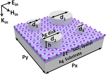
Schematic of metamaterials for multiband and broadband absorption enhancement of graphene at optical frequencies, which are composed of a graphene monolayer sandwiched between four Ag nanodisks and a SiO2 spacer on an Ag substrate. Geometrical parameters px and py are the array periods along the x and y directions, respectively; t is the thickness of the SiO2 spacer; d1, d2, d3, and d4 are the diameters of four Ag nanodisks (d1 > d2 > d3 > d4); h is the height of the Ag nanodisks. Ein, Hin, and Kin are the electric field, magnetic field, and wave vector of the incident light, which are along the x, y, and z axes, respectively
where ω is the frequency of incident light, e is electron charge, ħ is reduced Planck constant, Ef is Fermi energy (or chemical potential), τ is the relaxation time of electron-phonon, kB is Boltzmann constant, T is temperature in K, and i is the imaginary unit. Graphene has an anisotropic relative permittivity tensor of εg expressed as
| 2 |
where ε0 is the permittivity of the vacuum, and tg is the thickness of graphene sheet.
Results and Discussion
Figure 2 shows the calculated absorption spectra of graphene, Ag, and total metamaterials at normal incidence. One can clearly see four absorption peaks, whose resonance wavelengths are λ1 = 722.9 nm, λ2 = 655.7 nm, λ3 = 545.5 nm, and λ4 = 468.8 nm. At four absorption peaks, the light absorption in graphene can reach as high as 65.7, 61.2, 68.4, and 64.5%, respectively. Compared with a suspended monolayer graphene whose absorption efficiency is only 2.3% at optical frequencies [16, 17], the monolayer graphene in our designed metamaterials has an absorption enhancement of more than 26 times. It is also clearly seen in Fig. 2 that the absorbed light is mainly dissipated in graphene rather than in Ag. Moreover, the total absorption at the third peak exceeds 98.5%, very similar to much reported metamaterial electromagnetic wave perfect absorbers [69–75], which have many potential applications such as solar cells [76–81].
Fig. 2.
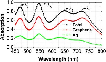
Normal-incidence absorption spectra of monolayer graphene (red circle), Ag (green triangle), and total metamaterials (black square) in the wavelength range from 450 to 800 nm. Geometrical and physical parameters: px = py = 400 nm, d1 = 140 nm, d2 = 110 nm, d3 = 80 nm, d4 = 50 nm, h = 50 nm, t = 30 nm, Ef = 0.50 eV, τ = 0.50 ps, T = 300 K, tg = 0.35 nm
To find the physical origins of above four absorption peaks, Figs. 3 and 4 plot the distributions of electric and magnetic fields at the resonance wavelengths of λ1, λ2, λ3, and λ4. At the resonance wavelength of λ1, the electric fields are mainly concentrated near the left and right edges of the first Ag nanodisk with a diameter of d1 (see Fig. 3a), and the magnetic fields are highly confined within the SiO2 region under the first Ag nanodisk (see Fig. 4a). Such field distributions correspond to the excitation of a magnetic dipole mode [82–86], which steps from the near-field plasmon hybridization between the first Ag nanodisk and the Ag substrate. At the resonance wavelengths of λ2, λ3, and λ4, the electromagnetic fields have the same distribution properties, but are localized in the vicinity of the second, third, and fourth Ag nanodisks with diameters of d2, d3, and d4, respectively. In short, the excitations of four independent magnetic dipole modes lead to the appearance of four absorption peaks in Fig. 2.
Fig. 3.
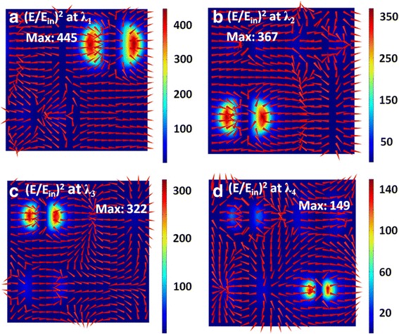
(a)-(d) Corresponding normalized electric field intensity (E/Ein) on the xoz plane across the center of the SiO spacer for the resonance wavelengths of λ , λ , λ , and λ labeled in Fig. 2. Red arrows represent the field direction, and colors show the field strength
Fig. 4.
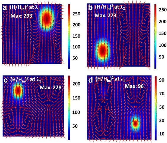
The same as in Fig. 3, but for normalized magnetic field intensity (H/Hin)2
In our designed metamaterials, the near-field plasmon hybridizations between individual Ag nanodisks and the Ag substrate form four independent magnetic dipole modes, which result into multiband absorption enhancement of monolayer graphene in the visible wavelength range from 450 to 800 nm, with an average absorption efficiency exceeding 50% (please see Fig. 2). The resonance wavelength of each magnetic dipole mode can be conveniently tuned by changing the diameter of the corresponding Ag nanodisk. If the diameters of the Ag nanodisks are varied for the absorption peaks in Fig. 2 to approach one another, a broad high-absorption band of monolayer graphene will be formed. To demonstrate this, Fig. 5a presents the normal-incidence absorption spectra of monolayer graphene, when the diameters d1, d2, d3, and d4 of four Ag nanodisks are equal to 110, 90, 70, and 50 nm, respectively. In this case, a broadband absorption enhancement in the wavelength range from 450 to 650 nm is achieved by the spectral design on the overlapped absorption peaks, with the lowest (highest) absorption efficiency more than 50% (73%). For the diameters of the Ag nanodisks to be increased gradually, this broad high-absorption band is red-shifted, as shown in Fig. 5b, c.
Fig. 5.
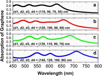
(a)-(d) Corresponding normal-incidence absorption spectra of monolayer graphene in the wavelength range from 450 to 800 nm with the diameters of four Ag nanodisks are varied, but the other parameters are the same as those in Fig. 2
Besides the diameters of the Ag nanodisks, we can tune the position of the absorption band in monolayer graphene by changing the thickness t of the SiO2 spacer. Figure 6 shows the normal-incidence absorption spectra in monolayer graphene, for t to be increased from 25 to 45 nm. With the increasing t, the absorption band in monolayer graphene will have an obvious blue-shift, because the near-field plasmon hybridizations between individual Ag nanodisks and the Ag substrate become weaker and thus magnetic dipole modes are blue-shifted [83].
Fig. 6.
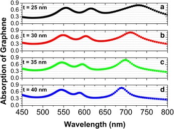
(a)-(d) Corresponding normal-incidence absorption spectra of monolayer graphene with the thickness of the SiO2 spacer increased from 25 to 40 nm in steps of 5 nm. The diameters of the Ag nanodisks are d1 = 140 nm, d2 = 120 nm, d3 = 100 nm, d4 = 80 nm, and the other parameters are the same as those in Fig. 2
In the above calculations, the coordinate points of four Ag nanodisks are (±px /4, ±py /4), so the center distance l between the nearest-neighbor Ag nanodisks is 200 nm. By varying l, we can also tune the position of the absorption band in monolayer graphene. Figure 7 gives the normal-incidence absorption spectra in monolayer graphene, for l to be decreased from 220 to 160 nm. With the decreasing l, the absorption band in monolayer graphene is slightly blue-shifted, owing to the plasmon interactions among the Ag nanodisks.
Fig. 7.
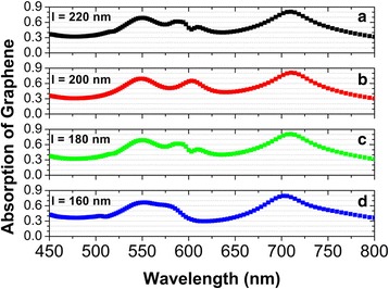
The same as in Fig. 6, but for the center distance l between the nearest-neighbor Ag nanodisks to be decreased from 220 to 160 nm
Conclusions
In this work, we have numerically investigated multiband and broadband absorption enhancement of monolayer graphene at optical frequencies from multiple magnetic dipole resonances in metamaterials. The unit cell of the metamaterials consists of a graphene monolayer sandwiched between four Ag nanodisks with different diameters and a SiO2 spacer on an Ag substrate. The near-field plasmon hybridizations between individual Ag nanodisks and the Ag substrate form four independent magnetic dipole modes, which result into multiband absorption enhancement of monolayer graphene in the visible wavelength range. When the magnetic dipole modes are tuned to be overlapped spectrally by changing the diameters of Ag nanodisks, a broadband absorption enhancement is achieved. The position of the absorption band in monolayer graphene can be also controlled, by varying the thickness of the SiO2 spacer or the distance between the Ag nanodisks. The numerical results may have some potential applications in optoelectronic devices, such as photodetectors.
Acknowledgements
This work is financially supported by the National Natural Science Foundation of China (NSFC) under Grant Nos. 11304159 and 11104136, the Natural Science Foundation of Zhejiang Province under Grant No. LY14A040004, the Natural Science Foundation of Jiangsu Province under Grant No. BK20161512, the Qing Lan Project of Jiangsu Province, the Open Project of State Key Laboratory of Millimeter Waves under Grant No. K201821, and the NUPTSF under Grant Nos. NY217045 and NY218022. J. Chen also acknowledges partial support from the National Research Foundation of Korea under “Young Scientist Exchange Program between The Republic of Korea and the People’s Republic of China”.
Availability of Data and Materials
All data are fully available without restriction.
Abbreviations
- 1D
One-dimensional
- 2D
Two-dimensional
- FDTD
Finite difference time domain
Authors’ Contributions
BL, CT, and JC contributed equally to this work. BL, CT, and JC performed the design, analyzed the data, and drafted the manuscript. CT, JC, and GP guided the idea and the simulations, and checked the figures. All authors read and approved the final manuscript.
Ethics Approval and Consent to Participate
We declare that there are no concerning data of human and animals.
Competing Interests
The authors declare that they have no competing interests.
Publisher’s Note
Springer Nature remains neutral with regard to jurisdictional claims in published maps and institutional affiliations.
Contributor Information
Bo Liu, Email: cjsliubo@163.com.
Chaojun Tang, Email: chaojuntang@126.com.
Jing Chen, Email: jchen@njupt.edu.cn.
Ningyan Xie, Email: 2624737484@qq.com.
Huang Tang, Email: tangh@126.com.
Xiaoqin Zhu, Email: zxq@jstu.edu.cn.
Gun-sik Park, Email: gunsik@snu.ac.kr.
References
- 1.Novoselov KS, Geim AK, Morozov SV, Firsov AA. Electric field effect in atomically thin carbon films. Science. 2004;306:666–669. doi: 10.1126/science.1102896. [DOI] [PubMed] [Google Scholar]
- 2.Ferrari AC, et al. Science and technology roadmap for graphene, related two-dimensional crystals, and hybrid systems. Nano. 2015;7:4598–4810. doi: 10.1039/c4nr01600a. [DOI] [PubMed] [Google Scholar]
- 3.Ye Y, Dai L, Gan L, Meng H, Dai Y, Guo XF, Qin GG. Novel optoelectronic devices based on single semiconductor nanowires (nanobelts) Nanoscale Res Lett. 2012;7:218. doi: 10.1186/1556-276X-7-218. [DOI] [PMC free article] [PubMed] [Google Scholar]
- 4.Lin F, Tong X, Wang YN, Bao JM, Wang ZMM. Graphene oxide liquid crystals: synthesis, phase transition, rheological property, and applications in optoelectronics and display. Nanoscale Res Lett. 2015;10:435. doi: 10.1186/s11671-015-1139-1. [DOI] [PMC free article] [PubMed] [Google Scholar]
- 5.Bao QL, Loh KP. Graphene photonics, plasmonics, and broadband optoelectronic devices. ACS Nano. 2012;6:3677–3694. doi: 10.1021/nn300989g. [DOI] [PubMed] [Google Scholar]
- 6.Koppens FHL, Mueller T, Avouris P, Ferrari AC, Vitiello MS, Polini M. Photodetectors based on graphene, other two-dimensional materials and hybrid systems. Nat Nanotechnol. 2014;9:780–793. doi: 10.1038/nnano.2014.215. [DOI] [PubMed] [Google Scholar]
- 7.Koppens FHL, Chang DE, de Abajo FJG. Graphene plasmonics: a platform for strong light-matter interactions. Nano Lett. 2011;11:3370–3377. doi: 10.1021/nl201771h. [DOI] [PubMed] [Google Scholar]
- 8.Grigorenko AN, Polini M, Novoselov KS. Graphene plasmonics. Nat Photonics. 2012;6:749–758. doi: 10.1038/nphoton.2012.262. [DOI] [Google Scholar]
- 9.Low T, Avouris P. Graphene plasmonics for terahertz to mid-infrared applications. ACS Nano. 2014;8:1086–1101. doi: 10.1021/nn406627u. [DOI] [PubMed] [Google Scholar]
- 10.de Abajo FJG. Graphene plasmonics: challenges and opportunities. ACS Photonics. 2014;1:135–152. doi: 10.1021/ph400147y. [DOI] [Google Scholar]
- 11.Vakil A, Engheta N. Transformation optics using graphene. Science. 2011;332:1291–1294. doi: 10.1126/science.1202691. [DOI] [PubMed] [Google Scholar]
- 12.Chen PY, Alu A. Atomically thin surface cloak using graphene monolayers. ACS Nano. 2011;5:5855–5863. doi: 10.1021/nn201622e. [DOI] [PubMed] [Google Scholar]
- 13.Ju L, Geng BS, Horng J, Girit C, Martin M, Hao Z, Bechtel HA, Liang XG, Zettl A, Shen YR, Wang F. Graphene plasmonics for tunable terahertz metamaterials. Nat Nanotechnol. 2011;6:630–634. doi: 10.1038/nnano.2011.146. [DOI] [PubMed] [Google Scholar]
- 14.Lee SH, Choi M, Kim TT, Lee S, Liu M, Yin X, Choi HK, Lee SS, Choi GG, Choi SY, Zhang X, Min B. Switching terahertz waves with gate-controlled active graphene metamaterials. Nat Mater. 2012;11:936–941. doi: 10.1038/nmat3433. [DOI] [PubMed] [Google Scholar]
- 15.Tassin P, Koschny T, Kafesaki M, Soukoulis CM. A comparison of graphene, superconductors and metals as conductors for metamaterials and plasmonics. Nat Photonics. 2012;6:259–264. doi: 10.1038/nphoton.2012.27. [DOI] [Google Scholar]
- 16.Nair RR, Blake P, Grigorenko AN, Novoselov KS, Booth TJ, Stauber T, Peres NMR, Geim AK. Fine structure constant defines visual transparency of graphene. Science. 2008;320:1308. doi: 10.1126/science.1156965. [DOI] [PubMed] [Google Scholar]
- 17.Dawlaty JM, Shivaraman S, Strait J, George P, Chandrashekhar M, Rana F, Spencer MG, Veksler D, Chen YQ. Measurement of the optical absorption spectra of epitaxial graphene from terahertz to visible. Appl Phys Lett. 2008;93:131905. doi: 10.1063/1.2990753. [DOI] [Google Scholar]
- 18.Liu JT, Liu NH, Li J, Li XJ, Huang JH. Enhanced absorption of graphene with one-dimensional photonic crystal. Appl Phys Lett. 2012;101:052104. doi: 10.1063/1.4740261. [DOI] [Google Scholar]
- 19.Pirruccio G, Moreno LM, Lozano G, Rivas JG. Coherent and broadband enhanced optical absorption in graphene. ACS Nano. 2013;7:4810–4817. doi: 10.1021/nn4012253. [DOI] [PubMed] [Google Scholar]
- 20.Ye Q, Wang J, Liu ZB, Deng ZC, Kong XT, Xing F, Chen XD, Zhou WY, Zhang CP, Tian JG. Polarization-dependent optical absorption of graphene under total internal reflection. Appl Phys Lett. 2013;102:021912. doi: 10.1063/1.4776694. [DOI] [Google Scholar]
- 21.Hashemi M, Farzad MH, Mortensen NA, Xiao SS. Enhanced absorption of graphene in the visible region by use of plasmonic nanostructures. J Opt. 2013;15:055003. doi: 10.1088/2040-8978/15/5/055003. [DOI] [Google Scholar]
- 22.Zhu JF, Liu QH, Linc T. Manipulating light absorption of graphene using plasmonic nanoparticles. Nano. 2013;5:7785–7789. doi: 10.1039/c3nr02660d. [DOI] [PubMed] [Google Scholar]
- 23.Zhao WS, Shi KF, Lu ZL. Greatly enhanced ultrabroadband light absorption by monolayer graphene. Opt Lett. 2013;38:4342–4345. doi: 10.1364/OL.38.004342. [DOI] [PubMed] [Google Scholar]
- 24.Stauber T, Gómez-Santos G, de Abajo FJG. Extraordinary absorption of decorated undoped graphene. Phys Rev Lett. 2014;112:077401. doi: 10.1103/PhysRevLett.112.077401. [DOI] [PubMed] [Google Scholar]
- 25.Grande M, Vincenti MA, Stomeo T, Bianco GV, de Ceglia D, Aközbek N, Petruzzelli V, Bruno G, De Vittorio M, Scalora M, D’Orazio A. Graphene-based absorber exploiting guided mode resonances in one-dimensional gratings. Opt Express. 2014;22:31511–31519. doi: 10.1364/OE.22.031511. [DOI] [PubMed] [Google Scholar]
- 26.Piper JR, Fan SH. Total absorption in a graphene monolayer in the optical regime by critical coupling with a photonic crystal guided resonance. ACS Photonics. 2014;1:347–353. doi: 10.1021/ph400090p. [DOI] [Google Scholar]
- 27.Dong B, Wang P, Liu ZB, Chen XD, Jiang WS, Xin W, Xing F, Tian JG. Large tunable optical absorption of CVD graphene under total internal reflection by strain engineering. Nanotechnology. 2014;25:455707. doi: 10.1088/0957-4484/25/45/455707. [DOI] [PubMed] [Google Scholar]
- 28.Grande M, Vincenti MA, Stomeo T, de Ceglia D, Petruzzelli V, De Vittorio M, Scalora M, D'Orazio A. Absorption and losses in one-dimensional photonic-crystal-based absorbers incorporating graphene. IEEE Photonics J. 2014;6:0600808. doi: 10.1109/JPHOT.2014.2356495. [DOI] [Google Scholar]
- 29.Miloua R, Kebbab Z, Chiker F, Khadraoui M, Sahraoui K, Bouzidi A, Medles M, Mathieu C, Benramdane N. Peak, multi-peak and broadband absorption in graphene-based one-dimensional photonic crystal. Opt Commun. 2014;330:135–139. doi: 10.1016/j.optcom.2014.05.043. [DOI] [Google Scholar]
- 30.Cai YJ, Zhu JF, Liu QH. Tunable enhanced optical absorption of graphene using plasmonic perfect absorbers. Appl Phys Lett. 2015;106:043105. doi: 10.1063/1.4906996. [DOI] [Google Scholar]
- 31.Niu J, Luo M, Zhu JF, Liu QH (2015) Enhanced plasmonic light absorption engineering of graphene: simulation by boundary-integral spectral element method. Opt Express 23:4539–4551 [DOI] [PubMed]
- 32.Grande M, Vincenti MA, Stomeo T, Bianco GV, de Ceglia D, Aközbek N, Petruzzelli V, Bruno G, De Vittorio M, Scalora M, D’Orazio A. Graphene-based perfect optical absorbers harnessing guided mode resonances. Opt Express. 2015;23:21032–21042. doi: 10.1364/OE.23.021032. [DOI] [PubMed] [Google Scholar]
- 33.Deng XH, Liu JT, Yuan JR, Liao QH, Liu NH. A new transfer matrix method to calculate the optical absorption of graphene at any position in stratified media. EPL. 2015;109:27002. doi: 10.1209/0295-5075/109/27002. [DOI] [Google Scholar]
- 34.Zheng GG, Zhang HJ, Xu YH, Liu YZ. Enhanced absorption of graphene monolayer with a single-layer resonant grating at the Brewster angle in the visible range. Opt Lett. 2016;41:2274–2277. doi: 10.1364/OL.41.002274. [DOI] [PubMed] [Google Scholar]
- 35.Long YB, Shen L, Xu HT, Deng HD, Li YX. Achieving ultranarrow graphene perfect absorbers by exciting guided-mode resonance of one-dimensional photonic crystals. Sci Rep. 2016;6:32312. doi: 10.1038/srep32312. [DOI] [PMC free article] [PubMed] [Google Scholar]
- 36.Lee YC, Lin KT, Chen HL. Ultra-broadband and omnidirectional enhanced absorption of graphene in a simple nanocavity structure. Carbon. 2016;108:253–261. doi: 10.1016/j.carbon.2016.07.012. [DOI] [Google Scholar]
- 37.Long YB, Li YX, Shen L, Liang WY, Deng HD, Xu HT. Dually guided-mode-resonant graphene perfect absorbers with narrow bandwidth for sensors. J Phys D Appl Phys. 2016;49:32LT01. doi: 10.1088/0022-3727/49/32/32LT01. [DOI] [Google Scholar]
- 38.Liu YJ, Xie X, Xie L, Yang ZK, Yang HW. Dual-band absorption characteristics of one-dimensional photonic crystal with graphene-based defect. Optik. 2016;127:3945–3948. doi: 10.1016/j.ijleo.2016.01.121. [DOI] [Google Scholar]
- 39.Zheng G, Cong JW, Chen YY, Xu LH, Xiao SR. Angularly dense comb-like enhanced absorption of graphene monolayer with attenuated-total- reflection configuration. Opt Lett. 2017;42:2984–2987. doi: 10.1364/OL.42.002984. [DOI] [PubMed] [Google Scholar]
- 40.Wang N, Bu LB, Chen YY, Zheng GG, Zou XJ, Xu LH, Wang JC. Multiband enhanced absorption of monolayer graphene with attenuated total reflectance configuration and sensing application. Appl Phys Express. 2017;10:015102. doi: 10.7567/APEX.10.015102. [DOI] [Google Scholar]
- 41.Guo J, Wu LM, Dai XY, Xiang YJ, Fan DY. Absorption enhancement and total absorption in a graphene-waveguide hybrid structure. AIP Adv. 2017;7:025101. doi: 10.1063/1.4975706. [DOI] [Google Scholar]
- 42.Wan Y, Deng LG (2017) Modulation and enhancement of optical absorption of graphene-loaded plasmonic hybrid nanostructures in visible and near-infrared regions. J Appl Phys 121: 163102
- 43.Huang FJ, Fu YQ. Theoretical T circuit modeling of graphene-based metamaterial broadband absorber. Plasmonics. 2017;12:571–575. doi: 10.1007/s11468-016-0299-x. [DOI] [Google Scholar]
- 44.Amin M, Farhat M, Bagci H. An ultra-broadband multilayered graphene absorber. Opt Express. 2013;21:29938–29948. doi: 10.1364/OE.21.029938. [DOI] [PubMed] [Google Scholar]
- 45.Yi SY, Zhou M, Shi X, Gan QQ, Zi J, Yu ZF. A multiple-resonator approach for broadband light absorption in a single layer of nanostructured graphene. Opt Express. 2015;23:10081–10090. doi: 10.1364/OE.23.010081. [DOI] [PubMed] [Google Scholar]
- 46.Shi X, Ge LX, Wen XW, Han DH, Yang YP. Broadband light absorption in graphene ribbons by canceling strong coupling at subwavelength scale. Opt Express. 2016;24:26357–26362. doi: 10.1364/OE.24.026357. [DOI] [PubMed] [Google Scholar]
- 47.He SL, Chen T. Broadband THz absorbers with graphene-based anisotropic metamaterial films. IEEE Trans Terahertz Sci Technol. 2013;3:757–763. doi: 10.1109/TTHZ.2013.2283370. [DOI] [Google Scholar]
- 48.Ning RX, Liu SB, Zhang HF, Bian BR, Kong XK. A wide-angle broadband absorber in graphene-based hyperbolic metamaterials. Eur Phys J Appl Phys. 2014;68:20401. doi: 10.1051/epjap/2014140221. [DOI] [Google Scholar]
- 49.Zhu ZH, Guo CC, Zhang JF, Liu K, Yuan XD, Qin SQ. Broadband single-layered graphene absorber using periodic arrays of graphene ribbons with gradient width. Appl Phys Express. 2015;8:015102. doi: 10.7567/APEX.8.072602. [DOI] [Google Scholar]
- 50.Huang XJ, Zhang X, Hu ZR, Aqeeli M, Alburaikan A. Design of broadband and tunable terahertz absorbers based on graphene metasurface: equivalent circuit model approach. IET Microw Antennas Propag. 2015;9:307–312. doi: 10.1049/iet-map.2014.0152. [DOI] [Google Scholar]
- 51.Khavasi A. Design of ultra-broadband graphene absorber using circuit theory. J Opt Soc Am B. 2015;32:1941–1946. doi: 10.1364/JOSAB.32.001941. [DOI] [Google Scholar]
- 52.Gao RM, Xu ZC, Ding CF, Wu L, Yao JQ. Graphene metamaterial for multiband and broadband terahertz absorber. Opt Commun. 2015;356:400–404. doi: 10.1016/j.optcom.2015.08.023. [DOI] [Google Scholar]
- 53.Wu PC, Papasimakis N, Tsai DP. Self-affine graphene metasurfaces for tunable broadband absorption. Phys Rev Appl. 2016;6:044019. doi: 10.1103/PhysRevApplied.6.044019. [DOI] [Google Scholar]
- 54.Yao G, Ling FR, Yue J, Luo CY, Luo Q, Yao JQ (2016) Dynamically electrically tunable broadband absorber based on graphene analog of electromagnetically induced transparency. IEEE Photonics J 8:7800808
- 55.Zhao YT, Wu B, Huang BJ, Cheng Q. Switchable broadband terahertz absorber/reflector enabled by hybrid graphene-gold metasurface. Opt Express. 2017;25:7161–7169. doi: 10.1364/OE.25.007161. [DOI] [PubMed] [Google Scholar]
- 56.Gao F, Zhu ZH, Xu W, Zhang JF, Guo CC, Liu K, Yuan XD, Qin SQ. Broadband wave absorption in single-layered and nonstructured graphene based on far field interaction effect. Opt Express. 2017;25:9578–9586. doi: 10.1364/OE.25.009579. [DOI] [PubMed] [Google Scholar]
- 57.Ye LF, Chen Y, Cai GX, Liu N, Zhu JF, Song ZY, Liu QH. Broadband absorber with periodically sinusoidally-patterned graphene layer in terahertz range. Opt Express. 2017;25:11223–11232. doi: 10.1364/OE.25.011223. [DOI] [PubMed] [Google Scholar]
- 58.Wang ZP, Hou YM. Ultra-multiband absorption enhancement of graphene in a metal-dielectric-graphene sandwich structure covering terahertz to mid-infrared regime. Opt Express. 2017;25:19185–19194. doi: 10.1364/OE.25.019185. [DOI] [PubMed] [Google Scholar]
- 59.Zhang Y, Shi Y, Liang CH. Broadband tunable graphene-based metamaterial absorber. Opt Mater Express. 2017;6:3036–3044. doi: 10.1364/OME.6.003036. [DOI] [Google Scholar]
- 60.Arik K, AbdollahRamezani S, Khavasi A. Polarization insensitive and broadband terahertz absorber using graphene disks. Plasmonics. 2017;12:393–398. doi: 10.1007/s11468-016-0276-4. [DOI] [Google Scholar]
- 61.Xiao BG, Gu MY, Xiao SS. Broadband, wide-angle and tunable terahertz absorber based on cross-shaped graphene arrays. Appl Opt. 2017;56:5458–5462. doi: 10.1364/AO.56.005458. [DOI] [PubMed] [Google Scholar]
- 62.Zhang YP, Li Y, Cao YY, Liu YZ, Zhang HY. Graphene induced tunable and polarization-insensitive broadband metamaterial absorber. Opt Commun. 2017;382:281–287. doi: 10.1016/j.optcom.2016.08.003. [DOI] [Google Scholar]
- 63.Deng BC, Guo QS, Li C, Wang HZ, Ling X, Farmer DB, Han SJ, Kong J, Xia FN. Coupling-enhanced broadband mid-infrared light absorption in graphene plasmonic nanostructures. ACS Nano. 2016;10:11172–11178. doi: 10.1021/acsnano.6b06203. [DOI] [PubMed] [Google Scholar]
- 64.Xia SX, Zhai X, Huang Y, Liu JQ, Wang LL, Wen SC. Multi-band perfect plasmonic absorptions using rectangular graphene gratings. Opt Lett. 2017;42:3052–19194. doi: 10.1364/OL.42.003052. [DOI] [PubMed] [Google Scholar]
- 65.Ying XX, Pu Y, Luo Y, Peng H, Li Z, Jiang YD, Xu J, Liu ZJ. Enhanced universal absorption of graphene in a Salisbury screen. J Appl Phys. 2017;121:023110. doi: 10.1063/1.4973898. [DOI] [Google Scholar]
- 66.Johnson PB, Christy RW (1972) Optical constants of the noble metals. Phys Rev B 6: 4370-4379
- 67.Zhu BF, Ren GB, Zheng SW, Lin Z, Jian SS. Nanoscale dielectric-graphene-dielectric tunable infrared waveguide with ultrahigh refractive indices. Opt Express. 2013;21:17089–17096. doi: 10.1364/OE.21.017089. [DOI] [PubMed] [Google Scholar]
- 68.Xiang YJ, Guo J, Dai XY, Wen SC, Tang DY. Engineered surface Bloch waves in graphene-based hyperbolic metamaterials. Opt Express. 2014;22:3054–3062. doi: 10.1364/OE.22.003054. [DOI] [PubMed] [Google Scholar]
- 69.Watts CM, Liu XL, Padilla WJ. Metamaterial electromagnetic wave absorbers. Adv Mater. 2012;24:OP98–OP120. doi: 10.1002/adma.201200674. [DOI] [PubMed] [Google Scholar]
- 70.Cui YX, He YR, Jin Y, Ding F, Yang L, Ye YQ, Zhong SM, Lin YY, He SL. Plasmonic and metamaterial structures as electromagnetic absorbers. Laser Photonics Rev. 2014;8:495–520. doi: 10.1002/lpor.201400026. [DOI] [Google Scholar]
- 71.Ra’di Y, Simovski CR, Tretyakov SA. Thin perfect absorbers for electromagnetic waves: theory, design, and realizations. Phys Rev Appl. 2015;3:037001. doi: 10.1103/PhysRevApplied.3.037001. [DOI] [Google Scholar]
- 72.Wang PW, Chen NB, Tang CJ, Chen J, Liu FX, Sheng SQ, Yan B, Sui CH. Engineering the complex-valued constitutive parameters of metamaterials for perfect absorption. Nanoscale Res Lett. 2017;12:276. doi: 10.1186/s11671-017-2048-2. [DOI] [PMC free article] [PubMed] [Google Scholar]
- 73.Liu ZQ, Liu GQ, Fu GL, Liu XS, Wang Y. Multi-band light perfect absorption by a metal layer-coupled dielectric metamaterial. Opt Express. 2016;24:5020–5025. doi: 10.1364/OE.24.005020. [DOI] [PubMed] [Google Scholar]
- 74.Liu ZQ, Liu XS, Huang S, Pan PP, Chen J, Liu GQ, Gu G. Automatically acquired broadband plasmonic-metamaterial black absorber during the metallic film-formation. ACS Appl Mater Interfaces. 2015;7(8):4962–4968. doi: 10.1021/acsami.5b00056. [DOI] [PubMed] [Google Scholar]
- 75.Liu XS, Chen J, Liu JS, Huang ZP, Yu MD, Pan PP, Liu ZQ. III-V semiconductor resonators: a new strategy for broadband light perfect absorbers. Appl Phys Express. 2017;10(11):111201. doi: 10.7567/APEX.10.111201. [DOI] [Google Scholar]
- 76.Wang Y, Zhou L, Zheng QH, Lu H, Gan QG, Yu ZF, Zhu J. Spectrally selective solar absorber with sharp and temperature dependent cut-off based on semiconductor nanowire arrays. Appl Phys Lett. 2017;110(20):201108. doi: 10.1063/1.4983711. [DOI] [Google Scholar]
- 77.Zhou L, Zhuang SD, He CY, Tan YL, Wang ZL, Zhu J. Self-assembled spectrum selective plasmonic absorbers with tunable bandwidth for solar energy conversion. Nano Energy. 2017;32:195–200. doi: 10.1016/j.nanoen.2016.12.031. [DOI] [Google Scholar]
- 78.Tang MY, Zhou L, Gu S, Zhu WD, Wang Y, Xu J, Deng ZT, Yu T, Lu ZD, Zhu J. Fine-tuning the metallic core-shell nanostructures for plasmonic perovskite solar cells. Appl Phys Lett. 2016;109(18):183901. doi: 10.1063/1.4966893. [DOI] [Google Scholar]
- 79.Zhou L, Tan YL, Wang JY, Xu WC, Yuan Y, Cai WS, Zhu SN, Zhu J. 3D self-assembly of aluminium nanoparticles for plasmon-enhanced solar desalination. Nat Photonics. 2016;10(6):393–398. doi: 10.1038/nphoton.2016.75. [DOI] [Google Scholar]
- 80.Zhou L, Tan YL, Ji DX, Zhu B, Zhang P, Xu J, Gan QQ, Yu ZF, Zhu J. Self-assembly of highly efficient, broadband plasmonic absorbers for solar steam generation. Sci Adv. 2016;2:e1501227. doi: 10.1126/sciadv.1501227. [DOI] [PMC free article] [PubMed] [Google Scholar]
- 81.Zhou L, Yu XQ, Zhu J. Metal-core/semiconductor-shell nanocones for broadband solar absorption enhancement. Nano Lett. 2014;14(2):1093–1098. doi: 10.1021/nl500008y. [DOI] [PubMed] [Google Scholar]
- 82.Liu B, Tang CJ, Chen J, Yan ZD, Zhu MW, Sui YX, Tang H. The coupling effects of surface plasmon polaritons and magnetic dipole resonances in metamaterials. Nanoscale Res Lett. 2017;12:586. doi: 10.1186/s11671-017-2350-z. [DOI] [PMC free article] [PubMed] [Google Scholar]
- 83.Hao J, Wang J, Liu X, Padilla WJ, Zhou L, Qiu M (2010) High performance optical absorber based on a plasmonic metamaterial. Appl Phys Lett 96: 251104
- 84.Song ZY, Zhang BL. Wide-angle polarization-insensitive transparency of a continuous opaque metal film for nearinfrared light. Opt Express. 2014;22:6519–6525. doi: 10.1364/OE.22.006519. [DOI] [PubMed] [Google Scholar]
- 85.Tang CJ, Yan ZD, Wang QG, Chen J, Zhu MW, Liu B, Liu FX, Sui CH. Ultrathin amorphous silicon thin-film solar cells by magnetic plasmonic metamaterial absorbers. RSC Adv. 2015;5:81866–81874. doi: 10.1039/C5RA15177E. [DOI] [Google Scholar]
- 86.Tang CJ, Yan B, Wang QG, Chen J, Yan ZD, Liu FX, Chen NB, Sui CH. Toroidal dipolar excitation in metamaterials consisting of metal nanodisks and a dielectric spacer on metal substrate. Sci Rep. 2017;7:582. doi: 10.1038/s41598-017-00708-5. [DOI] [PMC free article] [PubMed] [Google Scholar]
Associated Data
This section collects any data citations, data availability statements, or supplementary materials included in this article.
Data Availability Statement
All data are fully available without restriction.


