

Abstract
Homogeneous, single-crystal, monolayer epitaxial graphene (EG) is the one of most promising candidates for the advancement of quantized Hall resistance (QHR) standards. A remaining challenge for the electrical characterization of EG-based quantum Hall devices as a useful tool for metrology is that they are electrically unstable when exposed to air due to the adsorption of and interaction with atmospheric molecular dopants. The resulting changes in the charge carrier density become apparent by variations in the surface conductivity, the charge carrier mobility, and may result in a transition from n-type to p-type conductivity. This work evaluates the use of Parylene C and Parylene N as passivation layers for EG. Electronic transport of EG quantum Hall devices and non-contact microwave perturbation measurements of millimeter-sized areas of EG are both performed on bare and Parylene coated samples to test the efficacy of the passivation layers. The reported results, showing a significant improvement in passivation due to Parylene deposition, suggest a method for the mass production of millimeter-scale graphene devices with stable electrical properties.
Keywords: epitaxial graphene, quantum Hall effect, transport mobility, surface conductivity, Parylene
GRAPHICAL ABSTRACT
1. INTRODUCTION
Over the last few years, graphene has become a beacon to many scientific communities, partially because of its useful electrical properties.1–3 Graphene can be grown on silicon carbide (SiC) substrate by silicon sublimation, and it has been demonstrated that this form of graphene exhibits properties that make it appropriate for use in metrological applications like developing a quantized Hall resistance (QHR) standard.4–10 Developing this standard would require the properties of millimeter-scale EG devices, such as the surface conductivity, carrier density, and mobility to be relatively stable over time and unaffected by changes in the environment. Although millimeter-scale EG devices have already been realized for metrology, passivation efforts for devices of this size and application have not been heavily explored.11,12 Similar work has been reported for much smaller EG devices, but quantum Hall measurements were not monitored.13
If left exposed to air at ambient atmospheric conditions, the carrier density and surface conductivity of the unprotected EG varies over time.14–17 Because electrical stability is vital to the mass production of EG for other large-scale electrical applications, finding a suitable passivation material is a high priority. This holds especially true in the field of electrical metrology, where desired passivation entails electrical properties to be stable within unit percentages over several weeks in air. Efforts have been made to understand multiple forms of epitaxial graphene passivation, with some forms involving the use of poly-methyl methacrylate (PMMA),18 various dielectric materials available with atomic layer deposition tools,19–22 and amorphous boron nitride.13,23 One of the main issues with atomic layer deposition is the imparted carrier density by the various films, which span from 5×1012 cm−2 to 9×1012 cm−2. For resistance metrology, densities on order of 1012 or lower are required for epitaxial graphene devices to outperform the current standards based on gallium arsenide.
One possibility for passivation popular with organic field effect transistors and similar devices is Parylene, which shows excellent promise for stabilizing mass-producible electronics.24–29 In this work, we report on the use of Parylene C and Parylene N as encapsulating agents for EG. Their effectiveness to protect both EG quantum Hall devices and large areas of unprocessed monolayer EG is evaluated by remeasuring the electrical properties of samples after they have been exposed to various environmental conditions, such as a high temperature or high humidity. We report that Parylene C and N can passivate the surface conductivity to within 20 % of its previously measured value for EG areas on millimeter scales, and these results, despite not meeting the criterion for electrical resistance metrology, may have a more fruitful impact on general device engineering that does not rely on measuring resistances to one part in 108. A general, added advantage to using Parylene is that devices can be fully packaged and wire-bonded before deposition, enabling testing before process steps.
2. SAMPLE PREPARATION
2.1 High Temperature EG Growth
EG is formed by sublimating Si atoms from the surface of the SiC substrate’s Si face during an annealing process. Samples used for this study were grown both on square and rectangular SiC chips diced from 76 mm 4H-SiC(0001) semi-insulating wafers (CREE[see notes]) which has a miscut of about 0.10°. SiC chips were then submerged in a 5:1 diluted solution of hydrofluoric acid and deionized water, making an effective concentration of less than 10 %. Following a deionized water bath, chips were placed on top of a polished pyrolytic graphite substrate (SPI Glas 22[see notes]) with the SiC(0001) face resting against the graphite. The gap between the two surfaces creates a diffusion barrier for escaping Si atoms which promotes homogeneous graphene growth conditions.6 Some of the graphene samples were prepared with polymer-assisted sublimation growth.30 The annealing process was performed in ambient argon with a graphite-lined resistive-element furnace (Materials Research Furnaces Inc.[see notes]), with heating and cooling rates of about 1.5 °C/s. The growth chamber was evacuated and flushed with 100 kPa Ar from a 99.999 % liquid Ar source, and the growth stage was performed at 1900 °C.12 After growth, EG was checked with confocal laser scanning and optical microscopy to allow for quick identification of successful growth over large areas.31
2.2 Device Fabrication and Large Area EG Preparation
For electronic transport measurements, quantum Hall devices were fabricated in the same fashion as in previous works.12,13 In summary, a protecting layer of Au was placed on the chip prior to the multiple lithography steps required to etch out the Hall bar and its contact pads. Devices were fabricated on the smaller square chips measuring 7.6 mm by 7.6 mm while EG samples for microwave cavity perturbation measurements were etched into a well-defined rectangular shape, measuring 4.04 mm by 10 mm, on a chip whose dimensions were 15.2 mm by 7.6 mm. The shape of the EG area, which will be described in more detail later, was important for analyzing data from the microwave cavity measurements.
2.3 Parylene Deposition
For graphene encapsulation, two species of poly[para-xylylene], commonly known as Parylene C and Parylene N, were used in different sets of experiments and obtained from Specialty Coating Systems[see notes]. To deposit a layer with a thickness of 720 nm, a sub-gram amount of di-para-xylylene dimer was weighed and placed in an aluminum boat. For Parylene C and N, the contents of the boat were vaporized at 175 °C and 160 °C, respectively. The Parylene C and N was pyrolyzed at 690 °C and 650 °C to break the dimer and the resulting monomer para-xylylene was applied to the sample as a gas. The film was formed over a duration of about 6 hours by polymerization of the gaseous compounds on the cooled sample surface at 25 °C.
3. CHARACTERIZATION AND EXPERIMENTAL TECHNIQUES
3.1 Device Transport Measurements
Transport measurements of our EG devices were performed at 1.6 K in a 9 T superconducting magnet cryostat. Once the devices were fabricated, they were characterized by atomic force microscopy and Raman spectroscopy,32 and were mounted onto sample holders for magneto-transport measurements. The measurements were collected using a Labview[see notes] script to acquire I–V curves, magnetic field sweeps, and temperature data. The three main device characteristics of interest were longitudinal resistance (Rxx, or alternatively represented as sheet resistance ), device mobility (μ), and carrier density (ne). By measuring the Hall resistance (Rxy) as a function of the magnetic field, one can extract the carrier density by recalling the simple formula: . Furthermore, the mobility is linked to both the carrier density and the sheet resistance via: . In these formulas, e is the electron charge, W and L are the respective width and length of the Hall bar, and the derivative is approximated from a best-fit line of the Rxy voltages measured while sweeping the B-field through low values (< 1 T).
3.2 Environmental Exposure Conditions
After the sample was initially characterized, a series of various controlled environmental conditions were imposed on the samples, which included changes in both temperature and relative humidity. We used a Thermotron[see notes] testing chamber for these exposures since the chamber was able to maintain, for any given exposure, a stable temperature and humidity (within 0.1 % of the parameter value).
3.3 Non-Contact Resonance Microwave Cavity
For samples that were diced in a rectangular shape and have had limited fabrication, measurements were performed using an R100 air-filled standard rectangular waveguide cavity whose dimensions include a length of 127.0 mm, height of 10.16 mm, and width of 22.86 mm. The empty cavity shows the resonant frequency (f0) of the transverse electric field (TE103) mode of about 7.4350 GHz and the quality factor (Q0) in the range of 3200 at ambient conditions. Incremental insertion of the sample at the center of the waveguide, where the electric field attains a maximum value, allows one to extract the surface conductivity of a large, well-defined region of EG.33 The 0.5 mm incremental steps cause perturbations in the local electric field within the waveguide. Changes in the resonant frequency (fs) and quality (Qs) factor of the TE103 mode are then directly measured by a vector network analyzer connected to the cavity and recorded by VEE data acquisition software from Keysight.[see notes] The non-contact resonance microwave cavity allows one to extract the graphene surface conductivity, as demonstrated and described in other works.23,33 Accordingly, the fundamental equation for these measurements is given in the form:
| (1) |
In Equation 1, the variables are defined as such: Qs and Q0 are the quality factors of the perturbed and unperturbed case, respectively. The perturbed case is measured when a well-defined area of EG, having a width w and a variable height hx, is lowered into the cavity, causing a shift to a new frequency fx. The variables V0 and f0 are the total volume of the cavity and the unperturbed frequency of the TE103 mode, respectively. Aside from the constants ε0 (vacuum permittivity), 2b″ (depolarization contribution),34 and π, σEG remains as the surface conductivity of the EG and is elegantly taken to be the slope of Equation 1 once plotted. Measurements began when the slightest shift in the initial frequency was detected. Such a detection translates to approximately one part in 105 Hz.
4. RESULTS AND DISCUSSION
4.1 Parylene C and N Effects on EG Devices
To evaluate the effectiveness of Parylene passivation, two sets of tests are performed. The first test involves the passivation of fabricated quantum Hall devices. Before analyzing the results, it is important to recall the relation between the mobility and carrier density of the EG devices, which is shown in Reference 32. The general trend of the mobility is that it asymptotically reaches zero as ne goes to infinity, and the changes in mobility become subtler for higher ne. One can tune ne by using heat, humidity, or chemical treatment while the device is exposed to atmospheric conditions or vacuum.
Figure 1 shows a summary of how two types of Parylene passivation layers perform for preserving the sheet resistance and the mobility. The percentage difference is calculated after each process step, described below, to show the extent of modulation due to environmental exposure. The insets in the corners of the two graphs show the carrier density as a function of the process step for an example device coated with Parylene C and N. Several additional devices were measured using the same species of Parylene as the passivation layer, and the data, along with data from CYTOP encapsulation attempts, can be found in our additional work in Reference 32. For the devices in Figure 1, the process steps, with measurements collected between each step, are illustrated in Figure 2(a).
Figure 1.

The sheet resistance (green data points and axis) and mobility (purple data points and axis) are shown as a percentage change from their previous values after each process step. The insets show the example device’s carrier density measured as a function each step. The average modulations of the sheet resistance are shown as transparent, horizontal, green lines and represent the data after stabilization around process step 3.
Figure 2.

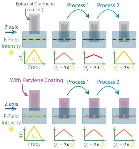
The process steps are illustrated here for clarity. All exposures to higher or lower temperatures take place over the course of 24 hours. (a) The first testing method is summarized for quantum Hall devices, with measurements being made between each process step. (b) The second testing method is slightly altered and lengthened for large-area graphene samples used in the microwave cavity.
Figure 1 shows the full monitoring of the sheet resistance and mobility, which reveals that, post-deposition and an initial drift of the electrical properties, Parylene C and N can passivate an EG quantum Hall device such that the sheet resistance (green axis and curves) modulates by a respective average of approximately 15 % and 8.3 % of its measured value when compared to its value prior to an environmental exposure. These averages provide a frame of reference for the second testing method that monitors the large-area surface conductivity, a quantity directly related to the sheet resistance. The modulation for the mobility (purple axis and curves) shown in Figure 1 reveal trends like those of the sheet resistance.
4.2 Parylene C and N Effects on Large Area Surface Conductivity
The second test for evaluating the effectiveness of Parylene passivation involved measuring elongated areas of EG (of dimensions 10 mm by 4.04 mm) with a microwave cavity, illustrated in Figure 3(a). EG surface conductivity values for exposed samples can modulate drastically by more than 100 %,23 and an example of this modulation manifesting itself in the measurement is shown in Figure 3(b). As the surface conductivity changes due to various environmental exposures, the slope of the microwave cavity electromagnetic wave perturbations tilts accordingly.
Figure 3.

(a) The experimental concept is depicted along with the change in the quality factor of the TE103 mode as the EG is inserted into the cavity. This change is roughly identical for EG areas coated by Parylene and very unsteady for bare EG which has been measured subsequently after various environmental exposures.23 (b) The manifestation of the drastic changes in quality factor is in our observation of the change of slope in Equation 1, which represents the surface conductivity of the EG. The orange, red, and gold colors used to mark the slopes are an illustrative representation of the similarly colored TE103 modes in (a). (c) The graphs representing the percent change in EG surface conductivity for both Parylene C and N are shown in orange and blue data points, respectively. The gray dotted line at the 20 % mark indicates that the regions below have identical vertical scales.
The surface conductivity data for passivated EG was obtained and plotted in Figure 3(c) for both types of Parylene. The process steps for the microwave cavity tests are illustrated in Figure 2(b). In these exposures, it appears that all changes to the surface conductivity are smaller than 20 % of the previously measured value, with Parylene N showing superior passivation. This passivation is very similar to the observed passivation in the sheet resistance during the first testing method.
When comparing these results to those from References 13 and 23, it appears that both Parylene and amorphous boron nitride have similar passivation capacities nearing 10 % to 15 %. Although the a-BN is significantly thinner a film than the Parylene, one cannot deposit it on a pre-packaged device, and this adds a significant disadvantage should device testing be desired before and after deposition.
5. CONCLUSION
In this work, the effectiveness of Parylene C and Parylene N as passivation layers for EG has been evaluated by two different testing methods, electronic transport of EG quantum Hall devices and the non-contact microwave perturbation measurements. The reported results showing EG electrical property passivation are significant for the mass production of millimeter-scale graphene devices with stable electrical properties.
Acknowledgments
Funding Sources
Work done by Y.Y. was supported by federal grant #70NANB12H185.
The work of C.-I.L and B.Y.W. at NIST was made possible by arrangement with Prof. C.-T. Liang of National Taiwan University. A.F.R and H.M.H would like to thank the National Research Council’s Research Associateship Program for the opportunity.
Footnotes
Notes
Commercial equipment, instruments, and materials are identified in this paper in order to specify the experimental procedure adequately. Such identification is not intended to imply recommendation or endorsement by the National Institute of Standards and Technology or the United States government, nor is it intended to imply that the materials or equipment identified are necessarily the best available for the purpose. The authors declare no competing financial interest.
References
- 1.Geim AK, Novoselov KS. The rise of graphene. Nat Mater. 2007;6:183–191. doi: 10.1038/nmat1849. [DOI] [PubMed] [Google Scholar]
- 2.Novoselov KS, Geim AK, Morozov SV, Jiang D, Zhang Y, Dubonos SV, et al. Electric field effect in atomically thin carbon films. Science. 2004;306:666–669. doi: 10.1126/science.1102896. [DOI] [PubMed] [Google Scholar]
- 3.Novoselov KS, Fal’ko VI, Colombo L, Gellert PR, Schwab MG, Kim K. A roadmap for graphene. Nature. 2012;490:192–200. doi: 10.1038/nature11458. [DOI] [PubMed] [Google Scholar]
- 4.Janssen TJBM, Tzalenchuk A, Yakimova R, Kubatkin S, Lara-Avila S, Kopylov S, et al. Anomalously strong pinning of the filling factor nu = 2 in epitaxial graphene. Phys Rev B. 2011;83:233402. [Google Scholar]
- 5.Fukuyama Y, Elmquist RE, Huang L-I, Yang Y, Liu F-H, Kaneko N-H. Controlling the Fermi Level in a Single-Layer Graphene QHE Device for Resistance Standard. IEEE Trans Instrum Meas. 2015;64:1451–1454. [Google Scholar]
- 6.Real MA, Shen T, Jones GR, Elmquist RE, Soons JA, Davydov AV. Graphene epitaxial growth on SiC(0001) for resistance standards. IEEE Trans Instrum Meas. 2013;62:1454–1460. [Google Scholar]
- 7.Lafont F, Ribeiro-Palau R, Kazazis D, Michon A, Couturaud O, Consejo C, et al. Quantum Hall resistance standards from graphene grown by chemical vapour deposition on silicon carbide. Nat Comm. 2015;6:6806. doi: 10.1038/ncomms7806. [DOI] [PMC free article] [PubMed] [Google Scholar]
- 8.Ribeiro-Palau R, Lafont F, Brun-Picard J, Kazazis D, Michon A, Cheynis F, et al. Quantum Hall resistance standard in graphene devices under relaxed experimental conditions. Nature Nanotechnol. 2015;10:965–971. doi: 10.1038/nnano.2015.192. [DOI] [PubMed] [Google Scholar]
- 9.Tzalenchuk A, Lara-Avila S, Kalaboukhov A, Paolillo S, Syväjärvi M, Yakimova R, et al. Towards a quantum resistance standard based on epitaxial graphene. Nat Nanotechnol. 2010;5:186–189. doi: 10.1038/nnano.2009.474. [DOI] [PubMed] [Google Scholar]
- 10.Janssen TJBM, Rozhko S, Antonov I, Tzalenchuk A, Williams JM, Melhem Z, et al. Operation of graphene quantum Hall resistance standard in a cryogen-free table-top system. 2D Mater. 2015;2:035015. [Google Scholar]
- 11.Novikov S, Lebedeva N, Pierz K, Satrapinski A. Fabrication and Study of Large-Area QHE Devices Based on Epitaxial Graphene. IEEE Trans Instrum Meas. 2015;64:1533–1538. [Google Scholar]
- 12.Yang G, Cheng Y, Mende P, Calizo IG, Feenstra RM, Chuang C, et al. Epitaxial Graphene Homogeneity and Quantum Hall Effect in Millimeter-Scale Devices. Carbon. 2017;115:229–236. doi: 10.1016/j.carbon.2016.12.087. [DOI] [PMC free article] [PubMed] [Google Scholar]
- 13.Rigosi AF, Liu C-I, Glavin NR, Yang Y, Hill HM, Hu J, Hight Walker AR, Richter CA, Elmquist RE, Newell DB. Electrical Stabilization of Surface Resistivity in Epitaxial Graphene Systems by Amorphous Boron Nitride Encapsulation. ACS Omega. 2017;2:2326. doi: 10.1021/acsomega.7b00341. [DOI] [PMC free article] [PubMed] [Google Scholar]
- 14.Yang Y, Huang L-I, Fukuyama Y, Liu F-H, Real MA, Barbara P, et al. Low Carrier Density Epitaxial Graphene Devices on SiC. Small. 2015;11:90–95. doi: 10.1002/smll.201400989. [DOI] [PubMed] [Google Scholar]
- 15.Ni ZH, Wang HMZQ, Luo ZQ, Wang YY, Yu T, Wu YH, et al. The effect of vacuum annealing on graphene. J Raman Spectroscopy. 2009;41:479–483. [Google Scholar]
- 16.Nomani MWK, Shields V, Tompa G, Sbrockey N, Spencer MG, Webb RA, et al. Correlated conductivity and work function changes in epitaxial graphene. Appl Phys Lett. 2012;100:092113. [Google Scholar]
- 17.Wehling TO, Novoselov KS, Morozov SV, Vdovin EE, Katsnelson MI, Geim AK, et al. Molecular doping of graphene. Nano Lett. 2008;8:173–177. doi: 10.1021/nl072364w. [DOI] [PubMed] [Google Scholar]
- 18.Lara-Avila S, Moth-Poulsen K, Yakimova R, Bjørnholm T, Fal’ko V, Tzalenchuk A, et al. Non-volatile photochemical gating of an epitaxial graphene/polymer heterostructure. Adv Mater. 2011;23:878–882. doi: 10.1002/adma.201003993. [DOI] [PubMed] [Google Scholar]
- 19.Hollander MJ, LaBella M, Hughes ZR, Zhu M, Trumbull KA, Cavalero R, et al. Enhanced transport and transistor performance with oxide seeded high-κgate dielectrics on wafer-scale epitaxial graphene. Nano Lett. 2011;11:3601–3607. doi: 10.1021/nl201358y. [DOI] [PubMed] [Google Scholar]
- 20.Robinson JA, LaBella M, Trumbull KA, Weng XJ, Cavelero R, Daniels T, et al. Epitaxial graphene materials integration: effects of dielectric overlayers on structural and electronic properties. ACS Nano. 2010;4:2667–2672. doi: 10.1021/nn1003138. [DOI] [PubMed] [Google Scholar]
- 21.Alaboson JMP, Wang QH, Emery JD, Lipson AL, Bedzyk MJ, Elam JW, et al. Seeding atomic layer deposition of high-k dielectrics on epitaxial graphene with organic self-assembled monolayers. ACS Nano. 2011;5:5223–5232. doi: 10.1021/nn201414d. [DOI] [PubMed] [Google Scholar]
- 22.Garces NY, Wheeler VD, Hite JK, Jernigan GG, Tedesco JL, Nepal N, et al. Epitaxial graphene surface preparation for atomic layer deposition of Al(2)O(3) J Appl Phys. 2011;109:124303-1–124303-6. [Google Scholar]
- 23.Rigosi AF, Glavin NR, Liu Y, Yang C-I, Obrzut J, Hill HM, Hu J, Lee H-Y, Hight Walker AR, Richter CA, Elmquist RE, Newell DB. Preservation of Surface Conductivity and Dielectric Loss Tangent in Large-Scale, Encapsulated Epitaxial Graphene Measured by Noncontact Microwave Cavity Perturbations. Small. 2017;13:1700452. doi: 10.1002/smll.201700452. [DOI] [PMC free article] [PubMed] [Google Scholar]
- 24.Nair S, Kathiresan M, Mukundan T, Natarajan V. Passivation of organic field effect transistor with photopatterned Parylene to improve environmental stability. Microelectron Eng. 2016;163:36–42. [Google Scholar]
- 25.Lee EK, Lee MY, Park CH, Lee HR, Oh JH. Toward Environmentally Robust Organic Electronics: Approaches and Applications. Adv Mater. 2017;1703638:1–29. doi: 10.1002/adma.201703638. [DOI] [PubMed] [Google Scholar]
- 26.Jakabovič J, Kováč J, Weis M, Hasko D, Srnánek R, Valent P, Resel R. Preparation and properties of thin parylene layers as the gate dielectrics for organic field effect transistors. Microelectron J. 2009;40:595–597. [Google Scholar]
- 27.Kahouli A, Sylvestre A, Ortega L, Jomni F, Yangui B, Maillard M, Berge B, Robert J-C, Legrand J. Structural and dielectric study of parylene C thin films. Appl Phys Lett. 2009;95:152901. [Google Scholar]
- 28.Sabri SS, Lévesque PL, Aguirre CM, Guillemette J, Martel R, Szkopek T. Appl Phys Lett. 2009;95:242104. [Google Scholar]
- 29.Unni KNN, Dabos-Seignon S, Nunzi J-M. Influence of the polymer dielectric characteristics on the performance of a quaterthiophene organic field-effect transistor. J Mater Sci. 2006;41:317. [Google Scholar]
- 30.Kruskopf M, Pakdehi DM, Pierz K, Wundrack S, Stosch R, Dziomba T, Götz M, Baringhaus J, Aprojanz J, Tegenkamp C. Comeback of epitaxial graphene for electronics: large-area growth of bilayer-free graphene on SiC. 2D Mater. 2016;3:041002. [Google Scholar]
- 31.Panchal V, Yang Y, Cheng G, Hu J, Liu C-I, Rigosi AF, Melios C, Kazakova O, Hight Walker AR, Newell DB, Elmquist RE. Rapid characterization of wafer-scale epitaxial graphene and graphene nanoribbons on SiC. 2017 arXiv:1711.03563. [Google Scholar]
- 32.Rigosi AF, Liu C-I, Wu BY, Lee H-Y, Kruskopf M, Yang Y, Hill HM, Hu J, Bittle EG, Obrzut J, Hight Walker AR, Elmquist RE, Newell DB. Quantum Hall Device Data Monitoring Following Encapsulating Polymer Deposition. Data in Brief. 2018;X doi: 10.1016/j.dib.2018.08.121. YYY. [DOI] [PMC free article] [PubMed] [Google Scholar]
- 33.Obrzut J, Emiroglu C, Kirillov O, Yang Y, Elmquist RE. Measurement. 2016;87:146. doi: 10.1016/j.measurement.2016.03.020. [DOI] [PMC free article] [PubMed] [Google Scholar]
- 34.Orloff ND, Obrzut J, Long CJ, Lam T, Kabos P, Novotny DR, Booth JC, Alexander Liddle J. IEEE Trans Microwave Theory Tech. 2014;62:2149. [Google Scholar]