Abstract
Layered metal phosphochalcogenides of molecular formula, MPX3 (M = Mn, Fe, Co, Ni, etc and X = S, Se) have been emerging as new class of semiconductors towards various catalytic and optoelectronic applications. The low cleavage energy associated with these layered chalcogenides may lead to devices with very thin semiconductor channels. Herein, we report the first successful fabrication of field effect transistor (FET) using layered NiPS3 that reveals n-type semiconducting behavior. Devices using bulk and few-layer NiPS3 with gold contacts show on/off ratios of ~103–105 at 25 °C. The device characteristics reveal an increase in on-state current with decrease in threshold voltage and the Schottky barrier height is extracted to be 112 meV. Density functional theory calculations reveal various parameters that affect electron/hole doping in the layered phosphochalcogenide material.
Introduction
Among the 2-dimensional layered materials, graphene has received considerable attention due to its ultrahigh mobility and tunability of layer thickness1,2. However, the zero band gap of pristine graphene limits its use in optoelectronics and other applications. Transition metal dichalcogenides (TMDs) such as MoS2 form the next class of well-studied compounds with certain band gap tunability3–12. Bulk MoS2 is semiconducting in nature with an indirect band gap of ~1.2–1.4 eV13, while mono-layer MoS2 possesses direct band gap of 1.8 eV14. This has led to various fundamental studies in the areas of electronic, optoelectronic and ultrasensitive sensors with atomically thin MoS2 membranes15–23. Though the TMDs (MoS2, WSe2) have shown high on/off ratios with tunable band gap in the visible wavelength range24,25, the low carrier mobility is of concern. Recently, phosphorene has been looked at, as a potential candidate for optoelectronic, electronic devices and sensors26–28, owing to its high on/off ratio coupled with high carrier mobility29,30. The disadvantage though is its stability that is still being tackled. Both TMDs and black phosphorus possess small band gaps thus restricting their applications in optoelectronics using light of short wavelength field effect transistors (FETs)20,26.
Continuous search for new 2D-materials has recently led to a well-studied class of bulk layered semiconducting metal phosphotrichalcogenides with formula MPX3 (M = Ni, Fe, Mn, Co, V, Zn etc; X = S and Se). This class of layered compounds have been wellexplored in the latter half of 20th century towards understanding their crystal structure and intercalation properties31–39. However, little is known as for as few layer MPX3 materials are concerned and recently, this area has been attracting considerable attention40–42 particularly towards catalysis43–47 and UV photodetector48. A recent review49 highlights the importance of this class of materials and their multifunctionality. The MPX3 family of materials possesses wide variation of band gap values from 1.3 eV to 3.5 eV. The cleavage energy of MPX3 is reported to similar and in certain cases, lower than that of graphene and TMDs41,50. Depending on the nature of metal ion, MPX3 family of compounds may open up ways to fabricate field effect transistors which is still a missing link in the current literature. A recent report on the first principle calculations on MnPSe3 reveals transformation from anti-ferromagnetic semiconductor to ferromagnetic half-metal by carrier doping37. Raman spectroscopic studies on certain stable MPX3 compounds has been recently reported40,41. However, electronic devices based on these classes of materials such as field effect transistors have not been explored in the literature so far.
Among the MPX3 family of semiconductors, NiPS3 is a layered ternary metal thiophosphate with monoclinic crystal system containing two molecular formula units per unit cell (Ni2P2S6), with point group, C2/m. NiPS3 is comprised of layers of covalently bonded units of (P2S6)4− bipyramids with honeycomb arrangement of divalent nickel ions. The sulfur atoms are hexagonally arranged along the c-axis in ABCABC sequence. The inter layers are connected through weak van der Waals forces similar to other layered 2D-materials such as TMDs. Hence, it is possible to separate the layers by mechanical exfoliation. Bulk NiPS3 is anti-ferromagnetic with magnetic moment of 3.9 BM51. The reported band gap of bulk NiPS3 is ~1.6 eV43.
In the present study, we have synthesized fairly large sized, oriented crystals of NiPS3 using a high temperature solid state method and explored its use in FETs. The material is thoroughly characterized using X-ray diffraction (XRD), Raman spectroscopy, transmission electron microscopy (TEM) and atomic force microscopy (AFM). Field effect transistors (FETs) have been fabricated and temperature dependent electrical transport measurements have been carried out. Density functional theory (DFT) calculations reveal the possible parameters that help understand the carrier-type observed in the electrical transport studies.
Result and Discussion
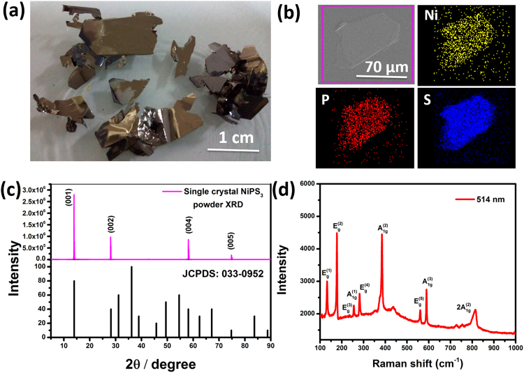
Highly oriented crystals of NiPS3 obtained in the present study are shiny black in colour with high crystallinity and the X-ray diffraction pattern shows very high orientation in the (00 l) direction. Figure 1(a–c) shows the optical images, scanning electron microscopic image with elemental mapping and the XRD pattern of large sized crystals. The Raman spectrum of the bulk material (Fig. 1d) shows a band at 253 cm−1 which is assigned to the A1g(1) mode. The high intense peak at 176 cm−1 is due Eg(2) vibration and the one observed at 384 cm−1 is due to symmetric stretching vibration of P-S bond in the P2S6 units (assigned as A1g(2)). The bands at 236 cm−1, 280 cm−1, 560 cm−1 and 588 cm−1 are assigned to Eg(3), Eg(4), Eg(5) and A1g(3) modes40,51,52. The bulk electrical conductivity has been measured to be 1.64 × 10⁻⁷ S/cm at 25 °C. TMDs such as 2H MoS2, MoSe2, WSe2 and MoTe2 show values of 3 × 10⁻², 2 × 10⁻¹, 6 and 1.8 S/cm respectively at 25 °C53.
Figure 1.
(a) Photographic images of NiPS3 crystals. (b) Scanning electron microscopic image with elemental mapping of mechanically exfoliated few layer NiPS3 on Si/SiO2 along with (c). XRD pattern of the bulk crystals and the corresponding standard pattern. (d) Raman spectrum of NiPS3 crystals obtained with 514 nm excitation laser.
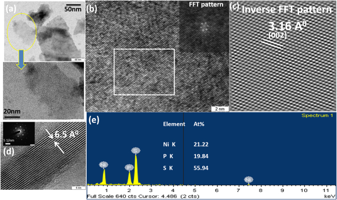
The trans conductance (gm) value of NiPS3 obtained from the fabricated FET devices is 2.5 µS/cm. The TMDs, on the other hand show values of 0.5–3 µS/µm for back-gated devices16. The morphology and microstructure of exfoliated NiPS3 nanosheets are given in Fig. 2. Spatially resolved EDS elemental mapping of Ni, P and S elements reveals a ratio of 1:1:3 as expected with uniform distribution of the elements obtained over the entire surface. The HRTEM image shows well-resolved lattice fringes along (002) plane, confirming the quality of the crystalline nanosheet (Fig. 2b). The selected area electron diffraction (SAED) pattern displays a single set of diffraction spots, further confirming the oriented nature of the exfoliated nanosheets (Fig. 2c).
Figure 2.
(a,b,d) High resolution TEM images of mechanically exfoliated few-layer NiPS3showing an interlayer spacing of 6.5 Å and the corresponding (c) FFT and (e) EDS mapping show the elemental ratio of Ni, P and S to be ~1:1:3.
The low cleavage energy41 reported for NiPS3 makes it possible to fabricate devices containing few to several layers of the material. The bulk crystals are exfoliated by mechanical means (Fig. S2) as reported for graphene-based materials54. The devices used in the present study are prepared by transferring the material onto pre-fabricated contact pads on highly doped silicon as the back gate with 230 nm SiO2 dielectric by standard mechanical exfoliation method using scotch tape. The source-drain metal contacts are given using 10/60 nm ITO/Au. The flakes in the devices have been characterized using optical microscopy, Raman spectroscopy (with excitation wave length of 514 nm) and the thickness is measured using atomic force microscopy (AFM). Several micron-sized, large flakeswith thicknesses ranging from 1.5–10 nm have been achieved in the devices. The characteristics discussed the present study are for devices with varying thicknesses of 1.5–60 nm consisting of 2–75 layers.
The back gated field effect transistors (FETs) have been fabricated and the characteristics followed. The data given below (Fig. 3) is for a channel length of 2.5 µm. The schematic of the FET along with the optical image, AFM picture and the height profile are shown in Fig. 3. It is clear that a large size single flake is present within the channel and the height is measured to be ~6.5 nm. This corresponds to 6 to 8 layers based on the single layer thickness of around 8 to 11 Å40. Standard transistor measurements have been carried out in vacuum (~10−5 mbar) and to ensure reproducibility, we have carried out measurements using several tens to hundreds of different devices.
Figure 3.
(a) Schematic of few-layer NiPS3 field effect transistor. (b) Optical micrograph of a typical NiPS3 device. (c) Atomic force microscopic image of 6.5 nm NiPS3 flake on Si/SiO2 with ITO/Au contact pads and the corresponding height profile measured across NiPS3 flake.
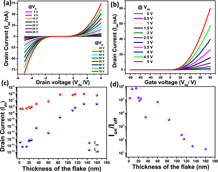
The on-off ratio, threshold voltage, carrier type and mobility have been evaluated. The output characteristics of the devices, source-drain voltage (Vds) vs. source-drain current (Ids) at different gate voltages are shown in Fig. 4. The non-linear behavior possibly arises due to the schottky barrier contact with Au metal. The current increases with increasing positive gate voltage, suggesting n-type semiconducting behavior. The on-off ratio estimated based onthe transfer characteristics is ~103–105 for most of the devices (Fig. 5) at 25 °C. The field effect mobility is extracted from the Ids-Vbg curve using the following expression5.
| 1 |
where μ is the mobility, W (3 μm) is the channel width, L (2.5 μm) is the channel length and Ci (1.5 × 10⁻⁴ F/m2) is the capacitance between the channel and the back gate per unit area (Ci = εoεr/d; εo = 8.85 × 10⁻¹² F⋅m−1; εr = 3.9; d = 230 nm). The mobility values are determined to be ~0.5–1 cm2/Vs. It is low as compared to several devices known in the literature. However, it is possible that poor contact with the metal electrode may be responsible as reported for MoS2 and WSe255,56. The mobility may be improved further by using high-K dielectric materials in top gated devices and is being presently studied.
Figure 4.
Electronic properties of few-layer NiPS3. (a) Drain current versus drain voltage for various Vg values as given in the figure, at 25 °C. (b) Drain current verses back gate voltage for Vds ranging from 0 to 5 V. The FET characteristics obtained for a flake thickness of 6.5 nm NiPS3. (c) Thickness dependent Ion (red) and Ioff (blue) currents. (d) Thickness dependence of Ion/Ioff ratio.
Figure 5.
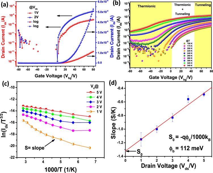
(a) Source-drain current as a function of gate voltage. (b) Temperature dependent transfer characteristics of the device. (c) Arrehenius plots of ln(Ids/T3/2) vs 1000/T. (d) Slope extracted from Fig. 5c as a function of Vds. ФB is derived from the y-intercept, S0.
A threshold voltage of 10 V is estimated by extrapolating the transfer characteristics. The Ion/Ioff ratio as a function of thickness of the material is shown in Fig. 4d and it is observed that for thicknesses less than 60 nm, the Ion/Ioff ~ 105 and it is of the order of 104–102 when the thickness is in the range 60–100 nm. Further increase in thickness leads to small Ion/Ioff ratio. This indirectly points to depletion length of ~100 nm for the present device. The Ion/Ioff ratio for MoS2 has been reported to be in the range of 107–101 for thicknesses varying from few nm to 250 nm57. The relationship between the depletion length with various parameters of the material is given below (Equation 2),
| 2 |
where, k is the Boltzmann constant, T is absolute temperature, q is elementary charge, εr is the vacuum permittivity, εs is the relative dielectric constant of NiPS3 (~9.2)58, ni is intrinsic carrier concentration 6 × 105 cm−3, and Nd is unintentional doping level. NiPS3 is known to be an intrinsic semiconductor with low conductivity59. For a depletion length of ~100 nm, the Nd works out to be 1.5 × 1017 cm−3 that points to certain level of doping in the material. It should be noted that NiPS3 possesses [P2S6]4− clusters that leads to ‘ionic’ interactions with Ni2+ in the material60. The contributions of thermionic emission current component (Ithermionic) and the thermally assisted tunneling current component (Itunneling) under different gate voltages indicate band bending at the metal - semiconductor interface. The Schottky barrier height (SBH) at the interface has been determined based on thermionic emission model using temperature dependent transport behavior. Figure 5b shows the devicecharacteristics at different temperatures and the change in current with the gate voltages is plotted (Fig. 5c) to extract the SBH using the following relationship (Equation 3).
| 3 |
where A is contact area of the junction, A* is the Richardson constant, q is magnitude of electron charge, ФB is the Schottky barrier height, kB is Boltzmann constant, n is ideality factor, Vds is drain-source voltage and T is the temperature. For the device shown in Fig. 3, the values of ln(Ids/T3/2) are plotted against 1000/T at different Vds as shown in Fig. 5c. The slope at each bias is determined and plotted as a function of source-drain bias as shown in Fig. 5d. The intercept observed in Fig. 5b is determined (S0). Using the equation 4,
| 4 |
the Schottky barrier height is calculated to be 112 meV for the 8 layer device of NiPS3. This value is similar to that observed for transition metal chalcogenide based devices21,61. Based on the small SBH determined from the transfer behavior, it may be expected that FET would show n-type unipolar behaviour and consequently the barrier height for holes is high [(band gap − SBH) for electrons].
FET devices based on bi-layer and bulk NiPS3
The output characteristics of the bi-layer NiPS3 device, source-drain voltage (Vds) vs. source-drain current (Ids) at different gate voltages are shown in Fig. S3. The current amplitude increases with increasing positive gate voltage as observed for the n-type behavior of eight-layer device. However, the current values for the bi-layer NiPS3 device are quite low as compared to the multilayer device. It has been reported by Kim and co-workers62 that density of states for multilayer MoS2 is several times larger than that of single layer MoS2 thus making multilayers attractive for device applications with considerable drain currents. The on-off ratio estimated based on the transfer characteristics is ~105 for the bi-layer devices and the mobility has been estimated to be ~0.5 cm2/Vs. The variation of mobility as a function of thickness of the flake (Fig. S4) is similar to the observations on reported TMD-based devices63. This is possibly due to scattering caused by extrinsic charge impurity that decreases as the number of layers increases, as reported for MoS263. The transport behavior for the device with 60 nm thick flake (Fig. S5) is similar to that observed for other thicknesses. The current values are large with on-off ratio and mobility of ~102–103 and ~3.5 cm2/Vs respectively.
DFT studies
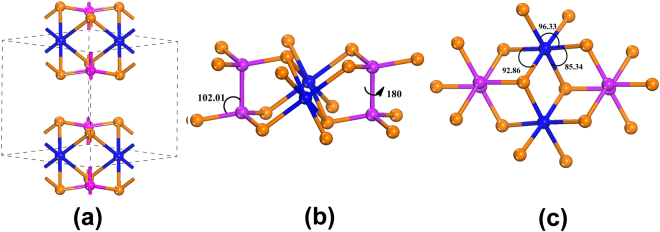
Density functional theory (DFT) calculations have been performed to decipher the electrical transport behavior of NiPS3. The crystal structure of NiPS3 (Fig. 6a) illustrates that the (P2S6)4− units are in staggered configuration where all sulphur atoms are coordinated to Ni in distorted octahedral environment and the van der Waals interlayer distance between S…S is 4.422 Å. The optimized geometry illustrates that the (P2S6)4− units show dihedral (angle involving S-P-P-S structure) angle of 180°. The six S-P-P angles in the (P2S6)4− unit being almost equal (Table S1), reveals that there is no strain present in the P2S6 clusters even when Ni is present in the lattice (Fig. 6b). On the contrary, the NiS610− units clearly reveal distortions in the structure. The distortion parameters (distortion angle, denoted as σ2oct)64–66 are measured as proposed by Robinson et al.67. Based on the structure (Fig. 6c), it is seen that there are twelve different bond angles that can be measured and the values are given in the Supporting Information (Table S1). The average σ2oct determined for neutral NiPS3 is 26.02°.
Figure 6.
(a) NiPS3 crystal structure showing various atom positions and van der Waals gap. (b) P2S64− units showing the dihedral angle of S-P-P-S and the angle of S-P-P. (c) NiS610− unit with different bond angles. Blue, pink and brown colours represent nickel, phosphorus and sulphur atoms respectively.
The DOS calculations (Fig. S6a) confirm the presence of up and down spins in the frontier region. The atom projected DOS given in Figure S7 indicates that the 3d bands of Ni (spin-up) are well-mixed with the 3p bands of S confirming strong hybridization as shown in SI (Fig. S6b,d). The upper valence bands are comprised of 3d orbital of Ni and 3p orbital of S. Sulphur dominates the valance band region whereas nickel contribution is maximum at the conduction band region. The orbital projected DOS of individual atoms reveals the presence of large population of 3p orbital of S at the Fermi whereas the contribution by phosphorus is very minimum. This may be due to the strong P-P covalent bond that appears in the lower valance band (−5 to −7 eV) energy region (Fig. S6c).
The FET characteristics of transistors and the type of conduction (p- or n-type) will depend on the relative position of the frontier region with respect to the metal contacts. To understand this aspect, the structural modulation of NiPS3 by electron/hole doping has been studied. The parameters obtained for the optimized geometries of neutral and hole/electron doped (0.1e− per atom) NiPS3 are given in the supporting information (Table S2 and S3 in SI). Same level of theory has been used to perform calculations in all the cases. Doping an electron (0.1e− per atom) to NiPS3 results in increased (8.01 eV) van der Waals gap and while for hole doping, the gap is found to be reduced (3.20 eV).
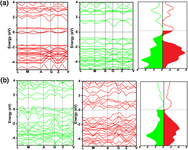
Addition of an electron elongates the Ni-S bond length and the opposite effect is observed by hole doping. Very little changes are observed in P-S and P-P bond lengths during electron and hole doping. Further, it is seen that the addition of electron decreases the bond angle distortion in the NiS6 octahedra quite considerably to nearly zero (1.5°) while the hole doping increases the distortion angle by 12° from the neutral value of 26.02°. This suggests that electron doping leads to stable octahedral geometry around Ni. The changes observed in NiS6 units confirm the earlier prediction based on DOS calculations that the doping affects the environment around Ni and S. In the case of electron doping, spin up bands illustrate that the conduction band minimum is observed at G k point and the valance band maximum is found in between L and M k point with a band gap of 1.53 eV while the spin down structure becomes metallic (Fig. 7a). Similarly, the hole doping makes it metallic in nature for spin-up configuration and semiconducting for spin-down configuration (Fig. 7b) with an indirect band gap of 0.47 eV. The results show that NiPS3 changes from semiconducting to metallic nature tuned by electron/hole doping. Magnitude of band gap may also indirectly indicate the stability of materials upon doping. This can be related to the spin flip-gap related stability on doping (Fig. S1).
Figure 7.
Band structure and total DOS of spin-up (green) and spin-down (red) configurations for (a) NiPS3 doped with 0.1 electron per atom, (b) NiPS3 doped with 0.1 hole per atom. The Fermi energy is set to zero.
The atom projected DOS for individual atoms with and without electron/hole doping are shown in Fig. S7. Ni dominates at the Fermi for electron doping while S dominates for hole doping. Interestingly, for electron doped structure, significant increase in the population of Ni is observed near Fermi as compared to neutral NiPS3. It has moved to lower energy region indicating that the structure stabilizes with electron doping. The Ni population decreases near Fermi and minor reduction at the valance band region is observed for the hole doped material. In the case of S, major changes occur only during hole doping. The above results indicate that the electron doping affects Ni and hole doping affects sulphur and consequently the NiS6 unit. This is supported by the lowered bond angle distortions during electron doping thus leading to stable NiS610− octahedral environment.
Summary
The present study has shown the possibilities of fabricating field effect transistors using layered phosphochalcogenides, NiPS3. The FET characteristics show n-type behavior with on/off ratio of 103–105. The DFT studies have predicted the transport characteristics and are experimentally verified. The phosphochalcogenides with magnetically active centers such as Ni, Co and Mn open ways to flip the spin behavior under magnetic field.
Experimental Section
Synthesis of NiPS3 crystals
Single crystals of NiPS3 have been synthesized by chemical vapor transport (CVT) technique using iodine as the transporting agent. Pure elements (99.99%) of nickel, phosphorous and sulphur (Aldrich) in stoichiometric proportions with I2 (2 mg/cc) were sealed in an evacuated quartz ampoule. After several attempts, the optimum reaction conditions were arrived at, with hot zone temperature of 950 °C and cold zone of 850 °C that result in high quality, large sized crystals of NiPS3. The schematics of CVT growth setup and the parameters used are given in the supporting information (Fig. S8, S9).
Characterization
The physicochemical nature of the crystals were identified using X-ray diffraction (XRD) (Philips, PAN analytical, with Cu-Kα radiation), transmission electron microscopy (TEM, JEOL 2100 F operating at 200 kV), Raman spectroscopy (LabRAM, Horiba, France, with excitation wavelength of 514.5 nm and 50x long working distance objective) and atomic force microscopy (AFM, Veeco, NanoscopeIVa Multimode AFM, with silicon nitride, Si3N4 probes of length 130 µm, width 35 µm, resonance frequency, 270 kHz and force constant, 4.5 N/m). The samples for TEM measurements were prepared by dispersing few-layer NiPS3 colloids onto carbon-coated copper grid and dried under vacuum. The electrical measurements were performed under high vacuum (<5 × 10⁻⁵) using Agilent B1500 semiconductor parametric analyzer. Devices were prepared by transferring the material onto pre-fabricated contact pads (Fraunhofer IPMS, Germany) on highly doped silicon with 230 nm SiO2 dielectric using standard mechanical exfoliation method. Source-drain metal contacts were given using 10/60 nm ITO/Au. Highly doped silicon act as the back gate. It was observed that the lithography procedure wherein the sample was exfoliated on Si/SiO2 surface and subsequently depositing the contact pads on the pre-marked areas led to sample deterioration due to the use of solvents during the process.
Computational methodology
Geometrical optimization calculations for all extended structures has been performed using VASP code68,69 with plane wave basis truncated at a kinetic energy of 500 eV. The projector augmented wave (PAW) scheme as incorporated in the Vienna ab initio simulation package (VASP) is used in the study (Supporting Information). Density of states and band structure calculations have been performed followed by optimization using CASTEP package70 including LDA + U approximation. Calculations have been performed for neutral NiPS3 and electron/hole doping separately, and the values are tabulated in Table S1 (Supporting Information).
Electronic supplementary material
Acknowledgements
The authors acknowledge the funding from Nanomission, DST, New Delhi, India. RNJ thanks UGC for a research fellowship.
Author Contributions
Ramesh Naidu Jenjeti synthesized the material and carried out FET studies. Rajat Kumar helped in carrying out certain transport measurements while Muthu P. Austeria carried out computational studies. S. Sampath conceived the research problem and all authors contributed in the interpretation of data and writing the manuscript.
Competing Interests
The authors declare no competing interests.
Footnotes
Electronic supplementary material
Supplementary information accompanies this paper at 10.1038/s41598-018-26522-1.
Publisher's note: Springer Nature remains neutral with regard to jurisdictional claims in published maps and institutional affiliations.
Contributor Information
Muthu P. Austeria, Email: muthu.austeria@gmail.com
S. Sampath, Email: sampath@iisc.ac.in
References
- 1.Geim AK, Novoselov KS. The Rise of Graphene. Nature Mater. 2007;6:183–191. doi: 10.1038/nmat1849. [DOI] [PubMed] [Google Scholar]
- 2.Novoselov KS, et al. Electric Field Effect in Atomically Thin Carbon Films. Science. 2004;306:666–669. doi: 10.1126/science.1102896. [DOI] [PubMed] [Google Scholar]
- 3.Chhowalla M, et al. The chemistry of two-dimensional layered transition metal dichalcogenide nano sheets. Nat. Chem. 2013;5:263–275. doi: 10.1038/nchem.1589. [DOI] [PubMed] [Google Scholar]
- 4.Novoselov KS, et al. Two-dimensional atomic crystals. Proc. Natl. Acad. Sci. 2005;102:10451–10453. doi: 10.1073/pnas.0502848102. [DOI] [PMC free article] [PubMed] [Google Scholar]
- 5.Radisavljevic B, Radenovic A, Brivio J, Giacometti V, Kis A. Single-layer MoS2 transistors. Nat. Nanotech. 2011;6:147–150. doi: 10.1038/nnano.2010.279. [DOI] [PubMed] [Google Scholar]
- 6.Huang X, Zeng Z, Zhang H. Metal Dichalcogenide Nanosheets: Preparation, Properties and Applications. Chem. Soc. Rev. 2013;42:1934–1946. doi: 10.1039/c2cs35387c. [DOI] [PubMed] [Google Scholar]
- 7.Xu M, Liang T, Shi M, Chen H. Graphene-Like Two-Dimensional Materials. Chem. Rev. 2013;113:3766–3798. doi: 10.1021/cr300263a. [DOI] [PubMed] [Google Scholar]
- 8.Ross JS, et al. Electrically tunable excitonic light-emitting diodes based on monolayer WSe2 p-n junctions. Nat. Nanoteh. 2014;9:268–272. doi: 10.1038/nnano.2014.26. [DOI] [PubMed] [Google Scholar]
- 9.Baugher BWH, Churchill HOH, Yang Y, Herrero PJ. Optoelectronic devices based on electrically tunable p-n diodes in a monolayer dichalcogenide. Nat. Nanotech. 2014;9:262–267. doi: 10.1038/nnano.2014.25. [DOI] [PubMed] [Google Scholar]
- 10.Splendiani A, et al. Emerging Photoluminescence in Monolayer MoS2. Nano Lett. 2010;10:1271–1275. doi: 10.1021/nl903868w. [DOI] [PubMed] [Google Scholar]
- 11.Lu J, et al. Improved Photoelectrical Properties of MoS2 Films after Laser Micromachining. ACS Nano. 2014;8:6334–6343. doi: 10.1021/nn501821z. [DOI] [PubMed] [Google Scholar]
- 12.Pospischil A, Furchi MM, Mueller T. Solar-energy conversion and light emission in an atomic monolayer p-n diode. Nat. Nanotech. 2014;9:257–261. doi: 10.1038/nnano.2014.14. [DOI] [PubMed] [Google Scholar]
- 13.Kam, K. K.& Parklnclon, B. A. Detailed Photocurrent Spectroscopy of the Semiconducting Group VI Transition Metal Dichaicogenides. J. Phys. Chem. 86, 463-467 (1982).
- 14.Mak KF, Lee C, Hone J, Shan J, Heinz TF. Atomically Thin MoS2: A New Direct-Gap Semiconductor. Phys. Rev. Lett. 2010;105:136805–136808. doi: 10.1103/PhysRevLett.105.136805. [DOI] [PubMed] [Google Scholar]
- 15.Wang QH, Zadeh KK, Kis A, Coleman JN, Strano MS. Electronics and optoelectronics of two-dimensional transition metal dichalcogenides. Nat. Nanotech. 2012;7:699–712. doi: 10.1038/nnano.2012.193. [DOI] [PubMed] [Google Scholar]
- 16.Cheng R, et al. Few-layer molybdenum disulfide transistors and circuits for high-speed flexible electronics. Nat. Commun. 2014;5:5143–5151. doi: 10.1038/ncomms6143. [DOI] [PMC free article] [PubMed] [Google Scholar]
- 17.Geim AK, Grigorieva IV. Van der Waals heterostructures. Nature. 2013;499:419–425. doi: 10.1038/nature12385. [DOI] [PubMed] [Google Scholar]
- 18.Duan X, et al. Lateral epitaxial growth of two-dimensional layered semiconductor heterojunctions. Nat. Nanotech. 2014;9:1024–1030. doi: 10.1038/nnano.2014.222. [DOI] [PubMed] [Google Scholar]
- 19.Cheng R, et al. Electroluminescence and Photocurrent Generation from Atomically Sharp WSe2/MoS2 Heterojunction p–n Diodes. Nano Lett. 2014;14:5590–5597. doi: 10.1021/nl502075n. [DOI] [PMC free article] [PubMed] [Google Scholar]
- 20.Lopez-Sanchez O, Lembke D, Kayci M, Radenovic A, Kis A. Ultrasensitive photodetectors based on monolayer MoS2. Nat. Nanotech. 2013;8:497–501. doi: 10.1038/nnano.2013.100. [DOI] [PubMed] [Google Scholar]
- 21.Das S, Chen H-Y, Penumatcha AV, Appenzeller J. High-Performance Multilayer MoS2 Transistors with Scandium Contacts. Nano Lett. 2013;13:100–105. doi: 10.1021/nl303583v. [DOI] [PubMed] [Google Scholar]
- 22.Sarkar, D. et al. MoS2 Field-Effect Transistor for Next Generation Label-Free Biosensors. ACS Nano. 8, 3992–4003 (2014). [DOI] [PubMed]
- 23.Roy K, et al. Graphene-MoS2 hybrid structures for multifunctional photoresponsive memory devices. Nat. Nanotech. 2013;8:826–830. doi: 10.1038/nnano.2013.206. [DOI] [PubMed] [Google Scholar]
- 24.Wang H, et al. Integrated Circuits Based on Bilayer MoS2 Transistors. Nano Lett. 2012;12:4674–4680. doi: 10.1021/nl302015v. [DOI] [PubMed] [Google Scholar]
- 25.Fang H, et al. High-Performance Single Layered WSe2 p-FETs with Chemically Doped Contacts. Nano Lett. 2013;12:3788–3792. doi: 10.1021/nl301702r. [DOI] [PubMed] [Google Scholar]
- 26.Kou L, Chen C, Smith SC. Phosphorene: Fabrication, Properties, and Applications. J. Phys. Chem. Lett. 2015;6:2794–2805. doi: 10.1021/acs.jpclett.5b01094. [DOI] [PubMed] [Google Scholar]
- 27.Lu J, et al. Bandgap Engineering of Phosphorene by Laser Oxidation toward Functional 2D Materials. ACS Nano. 2015;9:10411–10421. doi: 10.1021/acsnano.5b04623. [DOI] [PubMed] [Google Scholar]
- 28.Abbas AN, et al. Black Phosphorus Gas Sensors. ACS Nano. 2015;9:5618–5624. doi: 10.1021/acsnano.5b01961. [DOI] [PubMed] [Google Scholar]
- 29.Li L, et al. Black phosphorus field-effect transistors. Nat. Nanotechn. 2014;9:372–377. doi: 10.1038/nnano.2014.35. [DOI] [PubMed] [Google Scholar]
- 30.Das S, Demarteau M, Roelofs A. Ambipolar Phosphorene Field Effect Transistor. ACS Nano. 2014;8:11730–11738. doi: 10.1021/nn505868h. [DOI] [PubMed] [Google Scholar]
- 31.Lacroix PG, Clement R, Nakatani K, Zyss J, Ledoux I. Stilbazolium-MPS3, Nanocomposites with Large Second-Order Optical Nonlinearity and Permanent Magnetization. Science. 1994;263:658–660. doi: 10.1126/science.263.5147.658. [DOI] [PubMed] [Google Scholar]
- 32.Evans JSO, O’hure D. Kinetics of the Intercalation of Cations into MnPS3, Using Real Time In Situ X-Ray Diffraction. Adv. Mater. 1994;6:646–648. doi: 10.1002/adma.19940060904. [DOI] [Google Scholar]
- 33.Leflem G, Brec R, Ouvard G, Louisy A, Segransan P. Magnetic-interactions in the layer compounds MPX3 (M = Mn, Fe, Ni; X = S, Se) J. Phys. Chem. Solids. 1982;43:455–461. doi: 10.1016/0022-3697(82)90156-1. [DOI] [Google Scholar]
- 34.Clement R, Girerd JJ, Morgenstern-badarau I. Dramatic modification of the magnetic properties of lamellar MnPS3 upon intercalation. Inorg. Chem. 1980;19:2852–2854. doi: 10.1021/ic50211a079. [DOI] [Google Scholar]
- 35.Joy PA, Vasudevan S. Magnetism in the layered transition-metal thiophosphates MPS3 (M = Mn, Fe, and Ni) Phys. Rev. B. 1992;46:5425–5433. doi: 10.1103/PhysRevB.46.5425. [DOI] [PubMed] [Google Scholar]
- 36.Evans JSO, Ohare D, Clement R, Leaustic A, Thuery P. Origins of the spontaneous magnetization in MnPS3 intercalates-a magnetic-susceptibility and powder neutron diffraction study. Adv. Mater. 1995;207:735–739. doi: 10.1002/adma.19950070812. [DOI] [Google Scholar]
- 37.Li X, Wu X, Yang J. Half-metallicity in MnPSe3 exfoliated nanosheet with carrier doping. J. Am. Chem. Soc. 2014;136:11065–11069. doi: 10.1021/ja505097m. [DOI] [PubMed] [Google Scholar]
- 38.Rule KC, McIntyre GJ, Kennedy SJ, Hicks TJ. Single-crystal and powder neutron diffraction experiments on FePS3: search for the magnetic structure. Phys. Rev. B. 2007;76:134402–134408. doi: 10.1103/PhysRevB.76.134402. [DOI] [Google Scholar]
- 39.Leaustic A, et al. Constant-Machado H. High-T-c magnets in a series of substituted pyridinium–FePS3 layered intercalates. Chem. Mater. 1996;8:1954–1961. doi: 10.1021/cm960059y. [DOI] [Google Scholar]
- 40.Kuo C-T, et al. Exfoliation and Raman Spectroscopic Fingerprint of Few-Layer NiPS3 Van der WaalsCrystals. Sci. Rep. 2015;6:20904–20913. doi: 10.1038/srep20904. [DOI] [PMC free article] [PubMed] [Google Scholar]
- 41.Du K-Z, et al. Weak Van der Waals Stacking, Wide-Range Band Gap, and Raman Study on Ultrathin Layers of Metal Phosphorus Trichalcogenides. ACS Nano. 2016;10:1738–1743. doi: 10.1021/acsnano.5b05927. [DOI] [PubMed] [Google Scholar]
- 42.Long G, et al. Isolation and Characterization of Few-Layer Manganese Thiophosphite. ACS Nano. 2017;11:11330–11336. doi: 10.1021/acsnano.7b05856. [DOI] [PubMed] [Google Scholar]
- 43.Jenjeti RN, Austeria PM, Sampath S. Alternate to Molybdenum Disulfide: A 2D, Few-Layer Transition-Metal Thiophosphate and Its Hydrogen Evolution Reaction Activity over a Wide pH Range. ChemElectroChem. 2016;3:1392–1399. doi: 10.1002/celc.201600235. [DOI] [Google Scholar]
- 44.Li K, Rakov D, Zhang W, Xu P. Improving the intrinsic electro catalytic hydrogen evolution activity of few-layer NiPS3 by cobalt doping. Chem. Commun. 2017;53:8199–8202. doi: 10.1039/C7CC03173D. [DOI] [PubMed] [Google Scholar]
- 45.Mukherjee D, Austeria PM, Sampath S. Two-Dimensional, Few-Layer Phosphochalcogenide, FePS3: A New Catalyst for Electrochemical Hydrogen Evolution over Wide pH Range. ACS Energy Lett. 2016;1:367–372. doi: 10.1021/acsenergylett.6b00184. [DOI] [Google Scholar]
- 46.Konkena B, et al. Metallic NiPS3@NiOOH Core–Shell Heterostructures as Highly Efficient and Stable Electrocatalyst for the Oxygen Evolution Reaction. ACS Catal. 2017;7:229–237. doi: 10.1021/acscatal.6b02203. [DOI] [Google Scholar]
- 47.Wang F, et al. Two-dimensional Metal Phosphorus Trisulfide Nanosheet with Solar Hydrogen-Evolving Activity. Nano Energy. 2017;40:673–680. doi: 10.1016/j.nanoen.2017.09.017. [DOI] [Google Scholar]
- 48.Chu J, et al. High-Performance Ultraviolet Photodetector Based on a Few-Layered 2D NiPS3 Nanosheet. Adv. Funct. Mater. 2017;27:1701342. doi: 10.1002/adfm.201701342. [DOI] [Google Scholar]
- 49.Susner, M. A., Chyasnavichyus, M., McGuire, M. A., Ganesh, P. & Maksymovych, P. Metal Thio- and Selenophosphates as Multifunctional van der Waals Layered Materials. Adv. Mater. 1602852−1602891 (2017). [DOI] [PubMed]
- 50.Zhang, X., Zhao, X., Wu, D., Jing, Y. & Zhou, Z. MnPSe3 Monolayer: A Promising 2D Visible-Light Photohydrolytic Catalyst with High Carrier Mobility. Adv. Sci. 1600062-1600066 (2016). [DOI] [PMC free article] [PubMed]
- 51.Brec R. Review on structural and chemical properties of transition metal phosphorus trisulfides MPS3. Solid State Ionics. 1986;22:3–30. doi: 10.1016/0167-2738(86)90055-X. [DOI] [Google Scholar]
- 52.Berasconi M, Marra GL, Benedek G, Miglio L. Lattice dynamics of layered MPX3 (M = Mn, Fe, Ni, Zn; X = S, Se) compounds. Phy. Rev. 1998;B38:12089–12099. doi: 10.1103/physrevb.38.12089. [DOI] [PubMed] [Google Scholar]
- 53.El-Mahalawy SH, Evans BL. Temperature dependence of the electrical conductivity and hall coefficient in 2H-MoS2, MoSe2, WSe2, and MoTe2. Phys. Stat. Sol. (b) 1997;79:713–722. doi: 10.1002/pssb.2220790238. [DOI] [Google Scholar]
- 54.Huang Y, et al. Reliable Exfoliation of Large-Area High-Quality Flakes of Graphene and Other Two-Dimensional Materials. ACS Nano. 2015;9:10612–10620. doi: 10.1021/acsnano.5b04258. [DOI] [PubMed] [Google Scholar]
- 55.Feng Q, et al. Growth of Large-Area 2D MoS2(1−x)Se2x Semiconductor Alloys. Adv. Mater. 2014;26:2648–2653. doi: 10.1002/adma.201306095. [DOI] [PubMed] [Google Scholar]
- 56.Huang J, et al. Large-area Synthesis of Monolayer WSe2 on SiO2/Si Substrate and its Device Applications. Nanoscale. 2015;7:4193–4198. doi: 10.1039/C4NR07045C. [DOI] [PubMed] [Google Scholar]
- 57.Zhang Y, et al. Thickness Considerations of Two-Dimensional Layered Semiconductors for Transistor Applications. Sci. Rep. 2016;6:29615–29621. doi: 10.1038/srep29615. [DOI] [PMC free article] [PubMed] [Google Scholar]
- 58.Piacentini M, Khumalo FS, Olson CG, Anderegg JW, Lych DW. Optical transitions, XPS and electronic states in NiPS3. Chem. Phy. 1982;65:289–304. doi: 10.1016/0301-0104(82)85205-1. [DOI] [Google Scholar]
- 59.Foot PJS, Suradi J, Lee PA. Optical and electronic properties of the layered semiconductors NiPS3 and FePS3. Mat. Res. Bull. 1980;15:189–193. doi: 10.1016/0025-5408(80)90118-X. [DOI] [Google Scholar]
- 60.Foot PJS, et al. The Structures and Conduction Mechanisms of Lithium-Intercalated and Lithium-Substituted Nickel Phosphorus Trisulphide (NiPS3), and the Use of the Material as a Secondary Battery Electrode. Phys. stat. sol. (a) 1987;100:11–29. doi: 10.1002/pssa.2211000102. [DOI] [Google Scholar]
- 61.Chen J-R, et al. Control of Schottky Barriers in Single Layer MoS2 Transistors with Ferromagnetic Contacts. Nano Lett. 2013;13:3106–3110. doi: 10.1021/nl4010157. [DOI] [PubMed] [Google Scholar]
- 62.Kim S, et al. High-mobility and low-power thin-film transistors based on multilayer MoS2 crystals. Nat. Commun. 2012;3:1011–1017. doi: 10.1038/ncomms2018. [DOI] [PubMed] [Google Scholar]
- 63.Li S-L, et al. Thickness-Dependent Interfacial Coulomb Scattering in Atomically Thin Field-Effect Transistors. Nano Lett. 2013;13:3546–3552. doi: 10.1021/nl4010783. [DOI] [PubMed] [Google Scholar]
- 64.Alegria ECBA, et al. Mono-alkylation of cyanoimide at a molybdenum(IV) diphosphinic center by alkyl halides: synthesis, cathodically induced isomerization and theoretical studies. Electrochim. Acta. 2016;218:252–262. doi: 10.1016/j.electacta.2016.09.120. [DOI] [Google Scholar]
- 65.Ertl, A. et al. Polyhedron distortions in tourmaline. 40, 153–162 (2012).
- 66.Fop S, Wildman EJ, Skakle JMS, Ritter C, McLaughlin AC. Electrical and Structural Characterization of Ba3Mo1−xNb1+xO8.5−x/2: The Relationship between Mixed Coordination, Polyhedral Distortion and the Ionic Conductivity of Ba3MoNbO8.5. Inorg. Chem. 2017;56:10505–10512. doi: 10.1021/acs.inorgchem.7b01488. [DOI] [PubMed] [Google Scholar]
- 67.Robinson K, Gibbs GV, Ribbe PH. Quadratic Elongation: A Quantitative Measure of Distortion in Coordination Polyhedra. Science. 1971;172:567–570. doi: 10.1126/science.172.3983.567. [DOI] [PubMed] [Google Scholar]
- 68.Kresse G, Hafner J. Ab initio molecular dynamics for liquid metals. Phys. Rev. B. 1993;47:558–561. doi: 10.1103/PhysRevB.47.558. [DOI] [PubMed] [Google Scholar]
- 69.Kresse G, Hafner J. Ab initio molecular-dynamics simulation of the liquid-metal–amorphous-semiconductor transition in germanium. Phys. Rev. B. 1994;49:14251–14269. doi: 10.1103/PhysRevB.49.14251. [DOI] [PubMed] [Google Scholar]
- 70.Segall MD, et al. First-principles simulation: ideas, illustrations and the CASTEP code. Journal of Physics: Conden. Mat. 2012;14(11):2717–2744. [Google Scholar]
Associated Data
This section collects any data citations, data availability statements, or supplementary materials included in this article.


