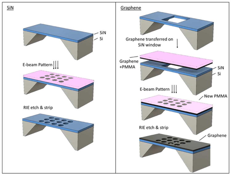
Figure 1. Schematic of EBL assisted RIE nanopore fabrication.

A) Fabrication process on SiN membrane. A 100 nm thick layer of PMMA is spin-coated on a SiN membrane prior to e-beam patterning. The pattern is transferred into the SiN membrane by reactive ion etching in a CHF3 plasma. Finally, the remaining resist is stripped in hot acetone (50°C) leaving a functional nanopore array. B) The same process on the graphene membrane. A graphene layer with a supporting PMMA layer is deposited on a pre-etched SiN window. The supporting layer of PMMA is stripped and a new 150 nm of PMMA is deposited prior to e-beam patterning. The pattern is transferred into the graphene membrane by reactive ion etching in an oxygen plasma. Finally, the remaining resist is stripped in m-xylene, leaving a functional nanopore array.
