Abstract
Purpose
We present a novel gamma‐ray‐detector design based on total internal reflection (TIR) of scintillation photons within a crystal that addresses many limitations of traditional PET detectors. Our approach has appealing features, including submillimeter lateral resolution, DOI positioning from layer thickness, and excellent energy resolution. The design places light sensors on the edges of a stack of scintillator slabs separated by small air gaps and exploits the phenomenon that more than 80% of scintillation light emitted during a gamma‐ray event reaches the edges of a thin crystal with polished faces due to TIR. Gamma‐ray stopping power is achieved by stacking multiple layers, and DOI is determined by which layer the gamma ray interacts in.
Method
The concept of edge readouts of a thin slab was verified by Monte Carlo simulation of scintillation light transport. An LYSO crystal of dimensions 50.8 mm × 50.8 mm × 3.0 mm was modeled with five rectangular SiPMs placed along each edge face. The mean‐detector‐response functions (MDRFs) were calculated by simulating signals from 511 keV gamma‐ray interactions in a grid of locations. Simulations were carried out to study the influence of choice of scintillator material and dimensions, gamma‐ray photon energies, introduction of laser or mechanically induced optical barriers (LIOBs, MIOBs), and refractive indices of optical‐coupling media and SiPM windows. We also analyzed timing performance including influence of gamma‐ray interaction position and presence of optical barriers. We also modeled and built a prototype detector, a 27.4 mm × 27.4 mm × 3.0 mm CsI(Tl) crystal with 4 SiPMs per edge to experimentally validate the results predicted by the simulations. The prototype detector used CsI(Tl) crystals from Proteus outfitted with 16 Hamamatsu model S13360‐6050PE MPPCs read out by an AiT‐16‐channel readout. The MDRFs were measured by scanning the detector with a collimated beam of 662‐keV photons from a 137Cs source. The spatial resolution was experimentally determined by imaging a tungsten slit that created a beam of 0.44 mm (FWHM) width normal to the detector surface. The energy resolution was evaluated by analyzing list‐mode data from flood illumination by the 137Cs source.
Result
We find that in a block‐detector‐sized LYSO layer read out by five SiPMs per edge, illuminated by 511‐keV photons, the average resolution is 1.49 mm (FWHM). With the introduction of optical barriers, average spatial resolution improves to 0.56 mm (FWHM). The DOI resolution is the layer thickness of 3.0 mm. We also find that optical‐coupling media and SiPM‐window materials have an impact on spatial resolution. The timing simulation with LYSO crystal yields a coincidence resolving time (CRT) of 200–400 ps, which is slightly position dependent. And the introduction of optical barriers has minimum influence. The prototype CsI(Tl) detector, with a smaller area and fewer SiPMs, was measured to have central‐area spatial resolutions of 0.70 and 0.39 mm without and with optical barriers, respectively. These results match well with our simulations. An energy resolution of 6.4% was achieved at 662 keV.
Conclusion
A detector design based on a stack of monolithic scintillator layers that uses edge readouts offers several advantages over current block detectors for PET. For example, there is no tradeoff between spatial resolution and detection sensitivity since no reflector material displaces scintillator crystal, and submillimeter resolution can be achieved. DOI information is readily available, and excellent timing and energy resolutions are possible.
Keywords: DOI, edge readout, optical barrier, PET
1. Introduction
Most current approaches to gamma‐ray detection can be divided into one of two general groups: direct detecting via semiconductors read out with charge‐transport‐sensing electrodes or indirect detecting via scintillators read out with photon‐transport‐sensing light sensors.1 Scintillator gamma‐ray detectors can be further divided into two strategies — continuous or monolithic‐crystal detectors and segmented‐crystal detectors (Fig. 1). For both continuous‐crystal and segmented‐crystal designs, photon sensors are usually attached to light guides that allow light from the exit face of the scintillator to spread into multiple sensors, yielding a data vector from which gamma‐ray interaction position can be decoded using Anger arithmetic or estimated using statistic‐based methods such as maximum‐likelihood estimation (ML).2 The monolithic‐crystal design can achieve relatively good spatial, energy, and timing resolution with crystals up to ~10–12 mm thickness, but with the thicker scintillator slabs required for stopping 511‐keV photons in positron emission tomography (PET), resolution is degraded and the probability of multiposition energy deposition by Compton scattering inside the scintillator slab increases. Also, the spatial resolution degrades and bias increases as the gamma‐ray interaction position approaches the crystal edges in designs that lack photon sensors near the edges.3, 4, 5
Figure 1.
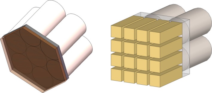
Left: Continuous‐scintillator detector. Right: Pixelated‐scintillator detector. [Color figure can be viewed at http://wileyonlinelibrary.com]
As a result, the PET block detectors based on arrays of ~3 mm × 3 mm × ~20‐mm segmented‐crystal arrays are the dominant technology in current clinical PET systems, offering good gamma‐ray stopping power (>80% gamma‐ray attenuated) and event positioning via crystal decoding with a modest number of readout channels. A review of the development of the block detector is provided in Lewellen (2008).5 Several groups have worked to make the pixel pitch very small to achieve ultra‐high spatial resolution, but typically at the expense of reduced sensitivity, crystal decoding precision, energy resolution, and/or timing resolution.5 Since reflectors separating crystal pixels are not detector material, their presence will reduce the detector's sensitivity, and multiposition energy deposition as a result of Compton scattering limits the smallest‐achievable spatial resolution in such designs. In addition, the cutting and surface treatment for crystal segmentation increases the total fabrication cost.5, 6, 7, 8, 9, 10
Semiconductor detectors can provide very good position resolution and superior energy resolution compared with scintillation detectors. Current room temperature semiconductors such as CdTe or CdZnTe have drawn great attention. But their relatively low timing resolution (~10 ns) due to slow charge collection has reduced their appeal as candidates for PET detectors. Since the low timing resolution requires an increased coincidence time window, a higher rate of random coincidences is recorded. Also, the relatively lower Z value requires a thicker detector and the fraction of photoelectric interactions is lower compared with inorganic scintillators such as LYSO.11, 12
The trend for future PET systems is continued improvement of spatial resolution, sensitivity, and image quality. Thus, it is important to develop PET detectors that have better energy resolution, depth‐of‐interaction (DOI) information, and subnanosecond timing for time‐of‐flight (TOF) reconstructions. Energy resolution is important for both scatter rejection and for helping to identify the first interaction point if there is Compton scattering inside the detectors, which improves image quality and spatial resolution, respectively.6, 12 DOI information is important because it can help reduce the parallax error, providing more uniform spatial resolution across the FOV. Also, the detector ring of a PET system can be made smaller when detectors yield DOI information, which brings additional benefits: a smaller detector ring will increase the solid angle coverage and improve the system's detection sensitivity;5 it will make the noncollinearity effect less severe and improve the physical spatial resolution limit; and it will reduce cost by reducing the number of required detector modules.
For continuous‐crystal scintillator detectors, DOI estimation has been demonstrated by analyzing the light response function (LRF), which requires careful calibration and statistical position‐estimation methods.3, 4 A great deal of effort has been devoted to enabling DOI estimation for block detectors. The Phoswich method utilizes the different decay times of different scintillators arranged in depth, which requires pulse‐shape‐discrimination (PSD) methods and circuit readout.13 Roncali et al. explored another PSD method by applying fluorescent paint on the crystal pixels, thus eliminating the need to use more than one type of scintillator and making PSD more compatible with time‐of‐flight technologies.14
The crystal shifting method applies lateral shifts across different crystal layers, changing the light response function (LRF) across different layers, and attempts to associate depth with lateral position; however, this method also increases the difficulty for decoding.15 Dual‐sided readouts have also been explored for DOI estimation, but at a cost of increased number of readout channels.16
TOF measurement is now feasible enabled by the development of faster and brighter scintillator materials and faster electronics. TOF helps to improve the image quality of reconstructed images for large patients and increases the contrast recovered during iterative reconstruction.17, 18, 19, 20, 21, 22 Current TOF systems usually have timing resolutions on the order of 300–600 ps,17 which corresponds to a location uncertainty of 45–90 mm along the line of response (LOR). Many research groups have now reported detectors with even better timing resolutions.18
In summary, to represent advances, PET detectors should have the following features: improved spatial resolution, improved energy resolution, improved detection sensitivity, DOI capability, and better than 500 ps timing resolution. We propose a detector design that has the potential to satisfy all of the requirements above.
2. Detector design concept
Inorganic scintillators usually have high indices of refraction;23 if a gamma‐ray photon is absorbed and has its energy converted into visible photons in a polished scintillator slab surrounded by air, most of these secondary photons will be confined inside the scintillator and transported to the edges by total internal reflection (TIR), as shown in Fig. 2. For an LYSO crystal, >80% of scintillation photons will be subject to TIR as their paths intersect the front and rear faces at angles beyond the critical angle and, thus, are reflected until they reach the edges. If linear arrays of photon sensors are attached to these edges, the energy and position of the gamma‐ray interaction position can be estimated from the set of signal amplitudes of the photon sensors using an estimator that incorporates the position‐dependent mean‐detector‐response functions (MDRFs) as determined from calibration measurements, light‐transport models, or a combination thereof.2
Figure 2.

Illustration of photon transport to the crystal edges via total internal reflection (TIR). Left: Only the photons emitted within the two cones have a chance to escape from the slab, all other photons are trapped inside the slab by TIR. Right: A calculation shows that with a critical angle of 33.8° (typical for LYSO), more than 80% of isotropically emitted photons reach an edge. [Color figure can be viewed at http://wileyonlinelibrary.com]
In some cases, it is advantageous to also create optical barriers (modifications that absorb/redirect optical photons) inside or on the surface of scintillator crystal to make the MDRFs sharper, thereby allowing interaction positions to be estimated with smaller variance (Fig. 3).
Figure 3.

A single layer of the proposed detector design. Left: 20 photon sensors (SiPMs) are attached to the edges of the scintillator crystal layer. The scintillator crystal has a 4 × 4 array of optical barriers. Right: Illustration of how optical barriers shape the mean‐detector‐response functions (MDRFs) critical for higher spatial resolution. [Color figure can be viewed at http://wileyonlinelibrary.com]
Multiple layers of relatively thin scintillator crystal, separated with small air gaps and light insulators (opaque absorbers to reduce crosstalk between adjacent layers), can be stacked together to increase gamma‐ray detection efficiency (Fig. 4). Depth‐of‐interaction (DOI) information can then be extracted by simply determining in which layer the gamma‐ray interaction occurred. This can be achieved by reading out directly, if the photon sensors are immediately optically coupled to each individual layer of scintillator (Fig. 4).
Figure 4.
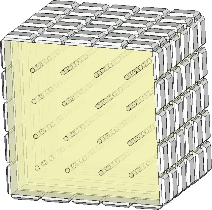
Multiple layers can be stacked as one detector module to increase gamma‐photon detection sensitivity. [Color figure can be viewed at http://wileyonlinelibrary.com]
If there is light guide between the scintillator crystal and the photon sensors, the DOI information can be determined by analysis of the relative signal strengths between layers of SiPMs (Fig. 5). The use of a peripheral light guide will lessen the ability to tile detectors adjacent to one another without gaps, and thus decrease the gamma‐ray detection sensitivity in a full system. Moreover, the use of light guides creates ambiguity if there is a multiposition energy deposition into different scintillator layers by Compton scatter. Therefore, we only discuss the design in Fig. 4, which we call the direct‐coupling method.
Figure 5.

Light guide can be used to share signals between layers for DOI estimation with a reduced number of readout channels, at a cost of increased dead areas. [Color figure can be viewed at http://wileyonlinelibrary.com]
3. Monte Carlo simulation
3.A. Simulation of Monolithic LYSO Detector Layer
In this section, a geometry to yield a practical PET detector module with edge readouts was simulated, to predict the performance it should achieve. A thin, square layer of LYSO crystal of dimension 50.8 mm × 50.8 mm × 3 mm was simulated. Twenty SiPMs were attached to the four edges of the crystal (five SiPMs on each edge of size: 10.16 mm × 3.0 mm, active area 10.0 mm × 3.0 mm, as shown in Fig. 3). The SiPMs’ spectrum‐averaged detection efficiency (PDE) was modeled as 20%; the dark‐count rate was modeled to be 1.0 MHz/mm2; the excess noise factor (ENF) was modeled as 1.21; and the readout shaping time was set to 150 ns. These parameters were chosen to be conservative, within the limits of performance specifications provided by several manufacturers. (Hamamatsu Photonics K. K., Hamamatsu City, Japan; Sensl, Inc., Cork, Ireland)
A portion of the photons arriving at the edges of the scintillation crystal are reflected by the SiPMs. Some reflected photons can be detected by other SiPMs, which would add variance to the position estimates. To assess the reflectance (the fraction of photons reflected) of an SiPM, a Hamamatsu 11827‐3344MG MPPC (SiPM) was measured in a Cary 5000 spectrometer. The spectral reflectance curve is shown in Fig. 6, and it varies from 0.15 to 0.30 over the spectral range of scintillation photons. The reflectance in the simulation was, therefore, set to 0.4 as a conservative estimate, and the type of reflection was modeled as specular. A lower refractive index of the optical‐gel/SiPM‐window material would also cause TIR at the edge surfaces for photons with large incident angles; in this part of simulation, we assumed that the refractive indices of the optical‐gel/SiPM‐window material were large enough (same as crystal) that the TIR effect at the edges could be neglected.
Figure 6.
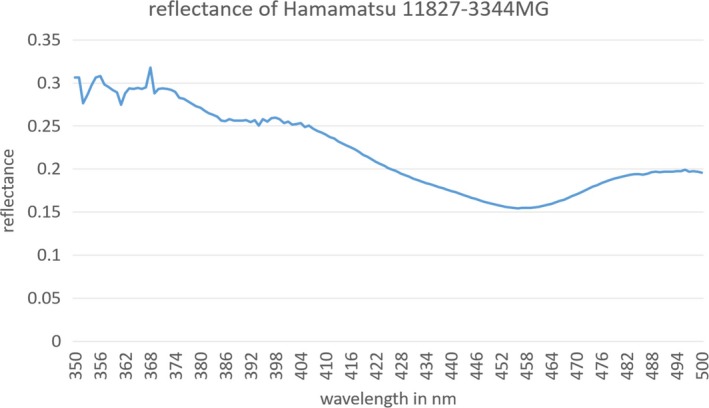
Spectral reflectance of a Hamamatsu 11827‐3344MG SiPM measured with Cary 5000 spectrometer. [Color figure can be viewed at http://wileyonlinelibrary.com]
The mean‐detector‐response functions (MDRFs) were computed by simulating the scanning of an ideally thin beam of 511‐keV gamma‐ray photons at a 252 × 252 array of sample positions across the detector area of 50.4 mm × 50.4 mm, yielding a step size of 0.2 mm. At each sample position, a total of 106 visible photons were modeled to be emitted uniformly into 4π steradians of solid angle, and had their trajectories tracked inside the crystal.
The front/back surfaces of the crystal slab were considered to be polished such that when a visible photon arrived at the front/back surfaces, the incident angle was compared with the critical angle of TIR; if the incident angle was larger than critical angle, the photon was reflected; otherwise, a random number uniformly sampled between [0, 1] was compared with the reflectance computed by the Fresnel equations. If it was smaller than the reflectance, the photon was reflected; otherwise, the photon was allowed to escape from the scintillation crystal.
If a visible photon reached one of the optical barriers, a random number uniformly sampled between [0, 1] was generated to be compared with the scattering (reflection/refraction) probability of the optical barrier. If the random number was smaller than the scattering probability of the optical barrier, it was considered to be scattered. Otherwise, it was considered to be absorbed or transmitted through the barrier.
The SiPMs were coupled to the edge surfaces with optical gel (or RTV silicone). At the interface between optical gel and scintillation crystal, TIR and Fresnel equations were considered to decide whether the photon was reflected or passed into the optical gel. As stated, in this part of simulation, the TIR at edge surfaces was neglected by choosing high‐refractive‐index optical‐gel and SiPM‐window material (refractive index of 1.82).
If the visible photon traveled into the optical gel and reached the window material of the SiPM, a random number uniformly sampled between [0, 1] was generated to be compared with the PDE and reflectance of the SiPM (0.2 and 0.4 in our simulation, respectively). If the random number was smaller than the PDE of SiPM (random number <=0.2), the photon was considered detected. Otherwise, if the random number was smaller than the value of sum of the PDE and reflectance of the SiPM (0.2 < random number <=0.6), the photon was reflected (specular reflection) back into the optical gel. If the random number was larger than the sum of PDE and reflectance (random number >0.6), it was considered absorbed but not detected.
The MDRFs are the position‐dependent ratio of the total counts on each SiPM divided by the total number of simulated visible photons (106). They can be scaled to simulate signals from any gamma‐ray energy.
For each gamma‐ray interaction, a total number of visible photons emitted by the interaction were modeled by sampling through a Gaussian distribution, with its mean set as the average number of visible photons per gamma‐ray interaction, and its standard deviation calculated from the intrinsic energy resolution reported for that scintillation crystal. With the total number of visible photons per gamma‐ray interaction, the counts on the SiPMs can be sampled from Poisson distributions, with their means equal to the total number of visible photons × MDRF(x, y, i), where x and y are the coordinates of the gamma‐ray photon interaction position, and i is the index of the SiPM. Finally, the variance of the Poisson‐distributed samples was increased by the excess noise factor (ENF). The MDRF(x, y, i) can be calculated by interpolation from the discrete MDRFs as mentioned in the above paragraph. Then, dark counts are added to each SiPM signal. The dark count for each SiPM is equal to the dark‐count rate (Hz/mm2) × active area (for each SiPM in mm2) × pulse shaping time(s).
3.B. Simulation case 1: without optical barriers
The MDRFs of the detector in Fig. 3 without optical barrier were simulated (Fig. 7). To evaluate the detector's performance, an ideally thin beam of 511‐keV gamma‐ray photons was modeled as scanning the detector at 20 × 20 sample positions, with a step size of 2.5 mm. A total of 1000 photoelectric gamma‐ray interactions were collected at each position. A contracting‐grid maximum‐likelihood search method was applied to estimate each event's interaction position in the detector.24 Figure 8 shows the resulting estimated image.
Figure 7.
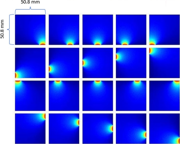
Simulated MDRFs of a 50.8 mm × 50.8 mm × 3.0 mm LYSO crystal without optical barriers. A total of 20 SiPMs are attached to edges (5 SiPMs on each edge).
Figure 8.
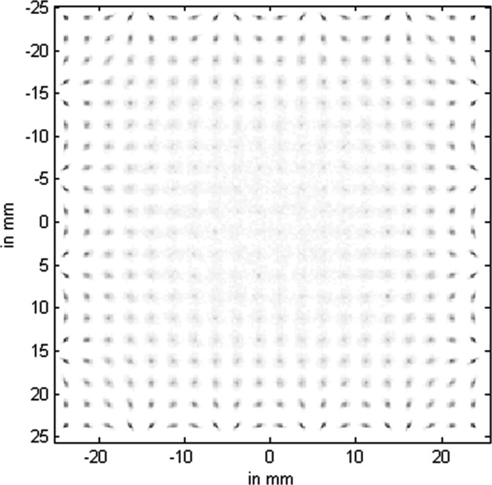
Estimated point‐grid image (its corresponding MDRFs are shown in Fig. 7, without optical barriers) of 20 × 20 positions (2 mm step size) by 511‐keV gamma‐ray photon beam.
3.C. Simulated case 2: with optical barriers
We define optical barriers as any photon absorbing/redirecting sites located inside or on the surface of the scintillation crystal that reshape the MDRFs. Optical barriers are effective because even a small shift of gamma‐ray interaction position near an optical barrier will cause the SiPMs’ signals to change greatly due to the magnified shifts of the “shadows” of the optical barriers (right‐hand side of Fig. 3). Two examples of optical barriers were explored in this work: mechanical holes as an example to illustrate the principle and laser‐etched patterns as a more desirable approach.
3.C.1. Mechanically drilled holes as optical barriers
A 4 × 4 array of holes (2 mm in diameter) drilled through the scintillation crystal act as partial diffuse reflectors, which means a fraction of arriving photons will be scattered diffusely by Lambertian reflection. We assumed the reflectance of the hole boundary to be 0.5 and the transmittance was assumed to be 0.0 for this simulation. The MDRFs of the thin piece detector (Fig. 3 with holes as optical barriers) were computed and shown in Fig. 9. A positioning map consisting of 1000 gamma‐ray photoelectric interactions at each of the 20 × 20 sample positions is shown in Fig. 10.
Figure 9.
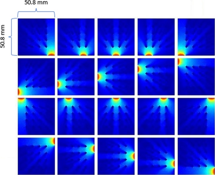
Simulated MDRFs of 50.8 mm × 50.8 mm × 3.0 mm LYSO crystal with 4 × 4 drilled‐hole optical barriers (2.0 mm diameter). Twenty SiPMs are attached on the edges (5 SiPMs on each edge).
Figure 10.
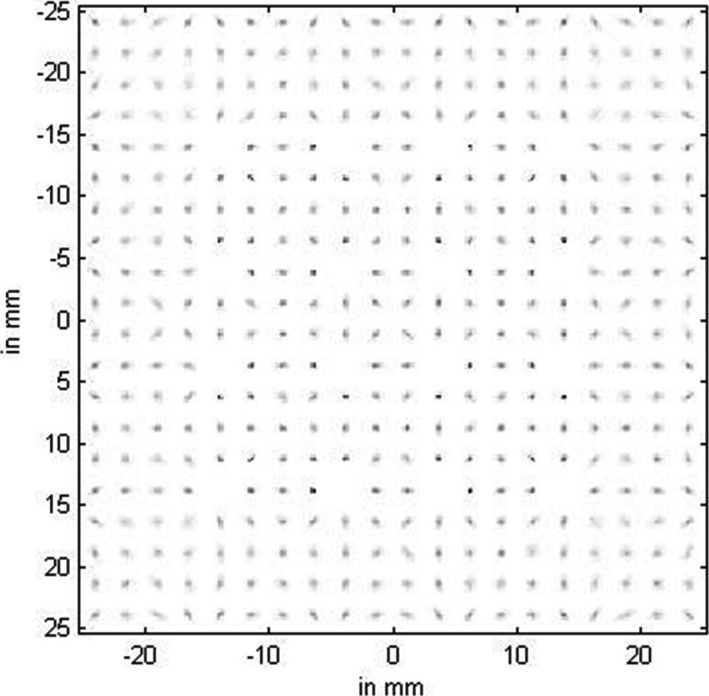
Estimated point‐grid image (its corresponding MDRFs are shown in Fig. 9, with drilled‐hole optical barriers) of 20 × 20 positions (2 mm step size) by 511‐keV gamma‐ray photon beam.
3.C.2. Laser‐etched patterns as optical barriers
The laser‐etching technique is quite mature; very fine patterns can be made in the crystal. It has already been used to etch pixel patterns in LYSO crystals.7, 8, 9, 10 Compared with mechanically drilled holes, laser etching will not remove scintillator material and, thus, avoids dead areas. In this simulation, the laser‐etched patterns were modeled as a series of semi‐transparent diffusive cylindrical surfaces (scattering probability 0.9, transmission probability 0.0, and absorption probability 0.1), with height equal to the thickness of the scintillation crystal. Scintillation photons arriving at the laser‐etched surfaces will be scattered in random directions or absorbed, and gamma‐ray interactions inside the laser‐etched cylinders will still be detected. The simulated MDRFs reshaped by laser‐etched patterns are shown in Fig. 11. A simulated positioning map is shown in Fig. 12.
Figure 11.
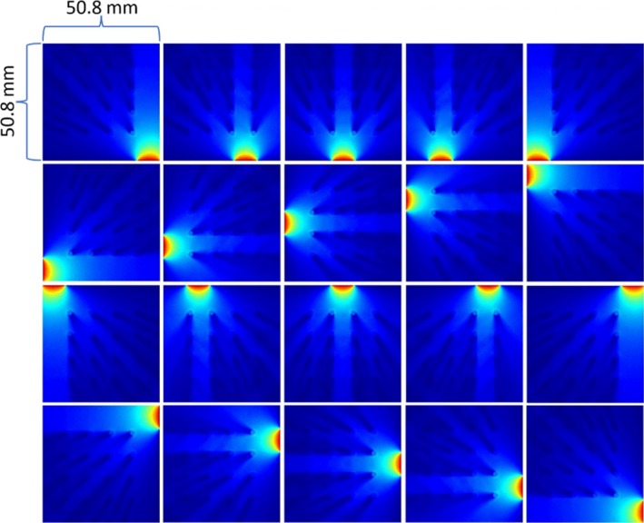
Simulated MDRFs of 50.8 mm × 50.8 mm × 3.0 mm LYSO crystal with 4 × 4 laser‐etched‐pattern optical barriers (2.0 mm diameter cylinder surface patterns). Twenty SiPMs are attached on edges (5 SiPMs on each edge).
Figure 12.

Estimated point‐grid image (its corresponding MDRFs are shown in Fig. 11, laser‐etched‐pattern optical barriers) of 20 × 20 positions (2‐mm step size) by 511‐keV gamma‐ray photon beam.
For position estimation with either type of optical barrier, the contracting‐grid search method no longer works well since there exist many local likelihood maxima in addition to the global maximum likelihood. Therefore, an exhaustive global search was used to estimate the events’ positions with optical barriers. More efficient algorithms can be developed as a two‐step process of getting close to the global maximum with a look‐up table before launching a small contracting‐grid search for the final stage.
3.D. Simulation of a smaller CsI/LYSO Detector Layer
We also simulated smaller crystals that we tested experimentally. The geometry of the scintillation crystal was set as 27.4 mm × 27.4 mm × 3.0 mm; 16 SiPMs were attached to the edges of the scintillation crystal with four SiPMs on each edge. Several factors influencing the spatial resolution were studied: (a) gamma‐ray photon energy and scintillator material (662 keV for CsI(Tl) vs 511 keV for LYSO); (b) optical barriers (with/without); (c) optical‐gel and SiPM‐window refractive indices (1.5 vs 1.82). The dark‐count rate was set to 2MHz/SiPM in accordance with the Hamamatsu S13360‐6050PE MPPC data sheet. The readout shaping time was set to 4us for CsI(Tl) and 150 ns for LYSO, based on their published decay times.25, 26 The optical‐gel/SiPM‐window materials’ refractive indices were studied to evaluate the effect of reflectance at the edge boundaries. The simulated resolutions (FWHM evaluated at 20 × 20 positions by a narrow beam of gamma‐ray photons) are shown in Table 1.
Table 1.
Factors that influence spatial resolution based on simulated data
| Spatial resolution factors | Edge‐coupling index 1.5 | Edge‐coupling index 1.82 | ||
|---|---|---|---|---|
| Without optical barriers | CsI(Tl) @ 662 keV | Whole | 0.67 ± 0.32 mm | 0.53 ± 0.18 mm |
| Center | 0.52 ± 0.12 mm | 0.71 ± 0.16 mm | ||
| LYSO @ 511 keV | Whole | 0.96 ± 0.45 mm | 0.75 ± 0.26 mm | |
| Center | 0.74 ± 0.17 mm | 1.0 ± 0.23 mm | ||
| With optical barriers | CsI(Tl) @ 662 keV | Whole | 0.41 ± 0.28 mm | 0.25 ± 0.14 mm |
| Center | 0.24 ± 0.10 mm | 0.25 ± 0.15 mm | ||
| LYSO @ 511 keV | Whole | 0.60 ± 0.40 mm | 0.35 ± 0.17 mm | |
| Center | 0.36 ± 0.15 mm | 0.36 ± 0.20 mm | ||
Whole: average spatial resolution of the whole detector region (27.4 mm × 27.4 mm). Center: average spatial resolution of the center region (15 mm × 15 mm). Edge‐coupling index: the refractive index of the optical‐gel and SiPM‐window material. ± indicates the standard deviation of spatial resolution across the tested detector area.
A slit beam of 662‐keV gamma photons was also simulated to verify our experiment described below. The width of the simulated beam was 0.44 mm (FWHM of a Gaussian profile). The resulting projection images for detectors without/with optical barriers are shown in Figs. 13 and 14, respectively.
Figure 13.
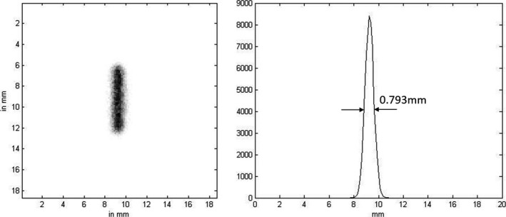
Left: Simulated projection image by a slit of width 0.44 mm. Right: profile with indicated FWHM, on the prototype detector (27.4 mm × 27.4 mm × 3.0 mm CsI(Tl), with 16 SiPMs) without optical barriers.
Figure 14.
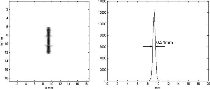
Left: Simulated projection image by a slit of width 0.44 mm. Right: Profile with indicated FWHM, on the prototype detector with drilled‐hole optical barriers.
4. Experimental verification
A prototype detector was built with a CsI(Tl) crystal of dimension 27.4 mm × 27.4 mm × 3 mm (obtained from Proteus, without/with mechanical holes), 16 Hamamatsu S13360‐6050PE MPPCs (SiPMs, size: 7.35 mm × 6.85 mm, active area: 6.0 mm × 6.0 mm), an AiT 16‐channel‐readout circuit, and corresponding 3D‐printed light‐tight cases and wires (Fig. 15). The scintillator was chosen to be CsI(Tl) for convenience (no background activity from the crystal and low hygroscopicity). The MDRFs were acquired by scanning the detector with a crossed‐slit‐collimated beam of 662 keV photons from a 137Cs source. The beam size on the detector surface was measured to be about 0.44 mm × 0.44 mm (FWHM) with an intensified quantum imaging detector (iQID) camera.27 Due to a limited dynamic range in the AiT readout electronics, only the center area of the detector was calibrated (15.0 mm × 15.0 mm) and used for imaging. The bias voltage of the SiPMs was set at 54.0 V, which is lower than the suggested bias voltage around 55.0 V.
Figure 15.
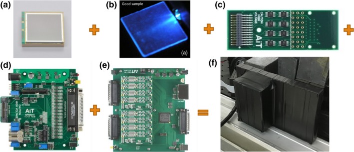
Key components of the prototype detector, including (a) 16 Hamamatsu S13360‐6050PE MPPCs (SiPMs); (b) CsI(Tl) scintillation crystal; (c) pre‐amplifier circuit; (d) amplifier circuit; (e) analog‐to‐digital converter and FPGA data acquisition circuit; (f) the assembled detector. [Color figure can be viewed at http://wileyonlinelibrary.com]
4.A. Experiment case 1: without optical barrier
The measured MDRFs of the CsI(Tl) crystal without optical barriers are shown in Fig. 16 (left). The MDRFs allow the best achievable spatial resolutions across the detector area to be predicted via calculation of the Cramér‐Rao lower bound on the mean variance in X‐ and Y‐direction,2 as shown in Fig. 16 (right). An experimentally acquired point‐grid image (similar to Figs. 8, 10, 12) is shown in Fig. 17 (left). A slit projection of 662‐keV photons of width 0.44 mm (FWHM of a Gaussian profile, as measured with the iQID camera) was used to experimentally evaluate the positioning performance. The resulting projection image is shown in Fig. 17 (middle).
Figure 16.

Left: Measured MDRF of the prototype detector without optical barriers, created by scanning a thin beam of 662‐keV gamma‐ray photons (0.44 mm × 0.44 mm, FWHM), in a regular array of positions across the detector. Right: The best spatial resolution achievable with these MDRFs, as predicted by calculation of the Cramér‐Rao lower bound on mean variance between X‐ and Y‐direction.
Figure 17.

Left: Point‐grid image measured by 0.44 mm × 0.44 mm gamma‐ray beam, step size is 1.5 mm, with 100 events per position, event on the MDRF boundary are piled up. Middle: Measured projection image by a slit of width 0.44 mm. Right: Profile with indicated FWHM, on the prototype detector (27.4 mm × 27.4 mm × 3.0 mm CsI(Tl), with 16 SiPMs) without optical barriers.
4.B. Experiment case 2: with optical barrier
With optical barriers, created by mechanically drilled holes (with Teflon lining the holes), the resolution can be greatly improved. The measured MDRFs are shown in Fig. 18 (left), and the spatial resolution map predicted by the Cramér‐Rao lower bound is shown in Fig. 18 (right). Again, an experimentally acquired point‐grid image is shown in Fig. 19 (left) and the performance was evaluated by a slit beam of 662‐keV photons of width 0.44 mm (FWHM). The resulting projection image is shown in Fig. 19 (middle). A position‐corrected (method described below) energy spectrum of a flood image by 137Cs is shown in Fig. 20.
Figure 18.
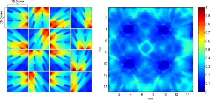
Left: Measured MDRF of the prototype detector with drilled‐hole optical barriers, created by scanning a thin beam of 662‐keV gamma photons across the central area of the detector. Right: The best spatial resolution achievable with these MDRFs, as predicted by Cramér‐Rao lower bounds on the mean variance of X‐ and Y‐direction.
Figure 19.

Left: Point‐grid image measured by 0.44 mm × 0.44 mm gamma‐ray beam, step size is 1.5 mm, with 100 events per position, event on the MDRF boundary are piled up. Middle: Measured projection image by a slit of width 0.44 mm. Right: Profile with indicated FWHM, on the prototype detector (27.4 mm × 27.4 mm × 3.0 mm CsI(Tl), with 16 SiPMs) with optical barriers.
Figure 20.

Measured spectrum of 137Cs acquired with the prototype detector with drilled‐hole optical barriers. Analog energy filter is applied to reject lower‐energy events.
5. Timing performance prediction
In order to assess the timing performance of the edge‐readout detector design, scintillation pulses were simulated for LYSO, LaBr3, and CsI(Tl) crystals (50.8 mm × 50.8 mm × 3.0 mm). Twenty SiPMs (10.0 mm × 3.0 mm) attached to the edges of the crystals were simulated with dark‐count rates of 1.0 MHz/mm2. The timestamp of each event was estimated using leading‐edge discrimination (LED), which consists of detecting when the signal crosses a constant threshold set above the noise level.
The steps to carry out the Monte Carlo timing simulations were as follows:
A gamma‐ray interaction produces scintillation photons at an interaction location in the crystal with an isotropic distribution of directions. The number of scintillation photons is a random variable determined by the energy deposited, characteristics of the scintillation crystal, and Poisson statistics as detailed in the Monte Carlo Simulation section above. Only interactions with full energy deposition of 511 keV were kept, and fractional energy depositions caused by Compton scatter were not considered in order to mimic the energy window of real experiments. The scintillation photon emission rates have exponential rise (τ ri) and exponential decay (τ di) components taken from the literature,25, 26 which are shown in Table 2. The emission time (relative to the time of interaction of a gamma ray) of each scintillation photon was sampled from a distribution determined by the exponential rise and decay time of the scintillator.
Scintillation photons were traced until they were detected or lost. Scintillation photons detected by an SiPM (with 20% PDE) were represented as a point process p(t) (represented numerically as a vector of integer numbers p[n]. If at a given time t a photon is detected, a “1” is added to p[t/∆t], where ∆t is the time step for the simulation, which is set to 10 ps). Also, the number of dark counts was sampled from a Poisson distribution with mean of Rdark*tshaping*Atotal. The time of each dark count was sampled from a uniform distribution in [0, tshaping]. Rdark is the dark‐count rate, tshaping is the pulse shaping time and Atotal is the total area of 20 SiPMs. These numbers are the same as those in Monte Carlo Simulation section, except that a shaping time for CsI(Tl) simulation was set to 4us. Lastly, the dark counts are superimposed on p(t).
The single cell response (SCR) f(t) of the SiPM was estimated from the data sheet of the Hamamatsu MCCP S13360‐6050PE.28 It was modeled as an exponential rise component with a rise‐time constant trise = 1 ns and an exponential decay component tdecay = 25 ns.
The scintillation pulse detected by a SiPM was modeled as the convolution of the point process p(t) and the SCR f(t).29
- The pulses from the 20 SiPMs were added to obtain one signal V(t) for each gamma‐ray event.
A timestamp was assigned to V(t).
Steps 1‐6 were repeated to obtain a distribution of timestamps for 1000 photoelectric interactions of 511‐keV gamma rays.
The coincidence resolving time (CRT) FWHM for two identical detectors was computed as 2.355√2 × standard deviation of the timestamps (Table 2).
Table 2.
Scintillator‐crystal parameters used to model photon emission rates and resulting simulated CRT FWHM.25, 26 % indicates the fraction of each rise/decay component. The threshold was set as a percentage of the mean pulse height
| trise (ns) | tdecay (ns) | CRT FWHM (ps) | |
|---|---|---|---|
| LaBr3 | 0.27 (72%)/2 (26%)/130 (2%) | 15.4 (100%) | 108 ± 6/0.7% |
| LYSO | 0.072 (100%) | 43 (100%) | 230 ± 11/0.7% |
| CsI(Tl) | 22.7 (100%) | 772 (61.1%)/3530 (38.7%) | 3300 ± 100/9.0% |
Since the timing performance depends on photon transport and is, therefore, potentially position dependent, five different event locations were analyzed: A = [0 mm, 0 mm] the center of the crystal, B = [−12.5 mm, 0 mm], C = [−25 mm, 0 mm], D = [−12.5 mm, −12.5 mm], and E = [−25 mm, −25 mm] (Fig. 21 (a)). The CRT is plotted as a function of the leading‐edge threshold level for a LYSO crystal with optical barriers in Fig. 21 (b) and without optical barriers in Fig. 21 (c). It is evident that the optical barriers do not significantly affect timing performance.
Figure 21.

(a) Timing performance was analyzed at 5 positions: A = [0 mm, 0 mm], B = [−12.5 mm, 0 mm], C = [−25 mm, 0 mm], D = [−12.5 mm, −12.5 mm], and E = [−25 mm, −25 mm]. (b) CRT FWHM for LYSO crystals with optical barriers. (c) CRT FWHM for LYSO crystals without optical barriers.
However, the mean time of the trigger does slightly depend on the gamma‐ray interaction position inside the detector since different interaction positions have different optical path distances to the light sensors. In our simulation, for the LYSO crystal with/without optical barriers, the worst case difference occurs when a gamma‐ray photon interacts in one of the edge‐readout detectors in the central part of the crystal (point A, Fig. 21 (a)), while the other annihilation gamma‐ray photon is absorbed in the corner part of the crystal of the opposing detector (point E, Fig. 21(a)). In this case, the systematic time difference is 49 ps without and 96 ps with optical barriers. However, this effect is minimal since the CRT is already approximately 200 ps. And, of course, a position‐dependent timing correction can easily be performed to eliminate this effect before TOF‐based image reconstruction.
6. Results
The Monte Carlo simulation indicates that the PET‐block‐detector‐sized design (50.8 mm × 50.8 mm × 3.0 mm LYSO crystal) can provide reasonable spatial resolution even without optical barriers (the average FWHM is 1.49 mm), and excellent spatial resolution with drilled‐hole optical barriers (the average FWHM is 0.56 mm) or laser‐etched pattern optical barriers (the average FWHM is 0.62 mm).
A further Monte Carlo simulation suggests that the optical‐gel/SiPM‐window materials’ refractive indices have a great impact on the detector's spatial resolution. Whether a photon has a chance to be reflected at the detector edge interface by undesired TIR is determined by the minimum refractive index encountered on its path from the scintillation crystal to the silicon substrate of the SiPM. As Table 1 shows, if the minimum refractive index on its path is 1.5, the overall spatial resolution will degrade by a few hundred micrometers. However, the central‐area spatial resolution may actually be improved due to the steepening of gradient features in the MDRFs in the center area, created by TIR at the edges. To understand this effect, one of the detector's (without optical barriers) simulated MDRFs for minimum refractive indices of 1.5 and 1.82 were compared (Fig. 22, left/middle). If the optical‐gel/SiPM‐window material had the lower index of 1.5 and a line connecting the gamma‐ray interaction position and the SiPM exceeded the TIR critical angle, then we observed a steep drop in the MDRF value and the spatial resolution degraded for events very close to each SiPM, especially in the corner regions of the crystal. If the optical‐gel/SiPM‐window material had the larger refractive index of 1.82, there was no TIR and the spatial resolution near edges was improved (Fig. 22, middle). We also found that optical barriers placed close to crystal boundaries provide an alternative means for improving the spatial resolution near the edges (Fig. 22, right), even in the absence of high‐index‐of‐refraction optical coupling, but at the expense of a more complicated MDRF shape.
Figure 22.
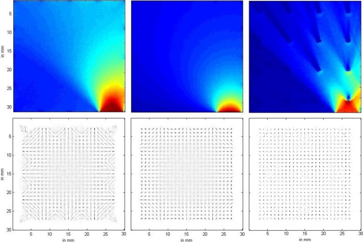
Top left: MDRF for refractive index of edge optical‐gel/SiPM‐window set to 1.5. Top middle: MDRF for the refractive index of 1.82. Top right: MDRF for the refractive index of 1.5, but with optical barriers close to edges. Bottom line, the corresponding point‐grid images (from left to right, respectively).
The experimental results demonstrated the potential of this detector design. The spatial resolution for the crystal without optical barriers was calculated based on the slit projection image. By summing along the vertical direction of Fig. 17 (middle), a profile plot is shown in Fig. 17 (right). The FWHM was measured to be 0.83 mm. Assuming the line‐spread function of the slit approximates a Gaussian profile, the spatial resolution (FWHM) is estimated to be: δ = (0.832 − 0.442)0.5 = 0.70 mm. For comparison, the simulated slit image of the prototype detector without optical barriers (Fig. 13) yielded a spatial resolution of: δsimulation ≈ 0.65 mm. The experimental result was a little worse to that predicted by simulation.
The procedure was repeated for the detector with optical barriers. The spatial resolution of the prototype detector with optical barriers was measured to be: δ experiment ≈ 0.39 mm, while the simulated resolution was predicted to be: δsimulation ≈ 0.31 mm. The measured spatial resolution is worse than that predicted by simulation, which is expected since the simulation does not include all electronic noise sources. Also, the spectral response curve of the Hamamatsu SiPM S13360‐6050PE is not optimal for CsI(Tl).
The energy resolution of the prototype detector with optical barriers was measured by exposing the detector to the 137Cs source without collimation. First a flood image was acquired, and each event's position in the flood image was estimated using the measured MDRF. Each event's summed‐SiPM‐signal value was also binned according to its estimated position. Then, the average energy at each position was calculated and stored in a 61 × 61 matrix (0.25‐mm step size). This matrix was used for position‐dependent energy correction. A second flood image was acquired that generated the energy spectrum including position‐dependent correction (Fig. 20). The FWHM energy resolution (ΔE/E) was estimated to be 6.4% at 662 keV, which is very good for a CsI(Tl) detector.30, 31 The energy spectrum in Fig. 20 was measured with a bias voltage of 54.0 V, lower than the 55.0 V suggested by the manufacturer. We observed no obvious nonlinear‐effect induced spectrum distortion due to SiPM saturation. The timing performance was predicted by Monte Carlo simulations; three different scintillation crystal materials with the same geometry were compared. The result in Fig. 21 shows that the CRT depends on the level of threshold for the leading‐edge discriminator, and that the introduction of optical barriers does not significantly affect the timing for TOF applications.
7. Discussion
The edge‐readout detector design can easily reach <1 mm resolution with the help of optical barriers, while simultaneously achieving good gamma‐ray detection efficiency via multiple layers, thus avoiding the usual tradeoff between spatial resolution and gamma‐ray detection sensitivity.1, 2 The energy resolution of this design is also excellent due to the large fraction of photons arriving at crystal edges. This feature could provide more effective discrimination against partial‐energy‐depositing Compton scattered events, which are undesired due to their degradation of both spatial and temporal resolution.2, 5, 6 Also, due to the monolithic design, there are no pixel gaps with reflective material, which further increases the gamma‐ray detection sensitivity. The direct DOI estimation gives this design even more advantages over traditional PET detectors, and multiposition energy‐deposition events across different layers caused by Compton scatter can, in principle, be identified. The first interaction position can often be estimated, from Compton kinematics which can help improve the spatial resolution. The effort of scintillator cutting and surface treatment is reduced due to the nonpixelated design. The detector design is also capable of working as a high‐sensitivity Compton camera for high‐energy gamma‐ray photons when outfitted with fast timing electronics. And finally, multiple modules can be tiled to produce cameras for SPECT.
Despite the numerous merits, there remain some challenges. One of the challenges is the large number of readout channels when multiple layers are combined. Figure 4 shows a 6‐layer design in which there are a total of 120 readout channels for a complete detector module. We are exploring strategies to both reduce the number of readouts and to develop compact FPGA‐based readout circuits to handle the large number of light sensors.
Another challenge is how to carry out the position estimation of each event quickly and accurately. When optical barriers are used, the MDRFs contain many sharp features that can create local likelihood maxima; there is a possibility that an ML search will be trapped in one of them. An exhaustive search is one solution, but is generally very slow. Algorithms, thus, need to be developed that can locate events’ positions quickly and accurately. We have previously demonstrated that parallelizing the positioning computations on GPUs is one very effective approach.2, 24
In addition, optimal timing performance and gain stability probably require SiPM cooling. This will increase the complexity and cost of the system somewhat. While we considered timing from the sum signal of all channels in a layer for simplicity, better performance may be possible with individual signals. Gain and noise‐level variations between different SiPMs and readout channels will require calibration, and the impact of uncorrected systematic effects could raise the timing uncertainty above the lower bound we report.
The introduction of optical barriers decreased the sensitivity by less than 2% in our simulation of the mechanically drilled version; an even smaller loss was noted with laser etching. A larger, but still acceptable, detection efficiency loss would be due to gaps between different detector modules if they are tiled to cover a large area, since the SiPMs and associated circuitry, even if mounted on polyimide, will be approximately 1.5 mm thick. For a crystal layer of 50.8 mm × 50.8 mm with ~3 mm gaps between adjacent detector modules, the sensitivity reduction is ~11%. However, the effect of gaps on reconstructed images can be minimized with use of staggered detector layers.32
Finally, the fast and accurate measurement of the calibration MDRFs for the detector remains a challenge, especially for LYSO crystals with self‐activity. We are devoting more effort to developing robust and fast methods to measure the MDRFs for this detector design.
8. Conclusion
The edge‐readout detector design exhibits many appealing features. These include excellent spatial resolution, good energy resolution, and the ability to recover DOI information. The high 3D resolution of this prototype design is immediately appealing for specialized clinical applications such as human brain PET and preclinical PET. However, the challenges of large number of readout channels and fast MDRF measurement still need to be addressed.
Conflicts of interest
The authors have no conflicts of interest to disclose.
Acknowledgments
The authors thank H. Bradford Barber, Ryeojin Park, Ling Han, and Brian W. Miller for helpful discussions. This work was partially supported by NIH/NIBIB grant P41‐EB002035 “The Center for Gamma‐Ray Imaging.” M. Ruiz‐Gonzalez was supported in part by the Mexican National Council of Science and Technology, and in part by the Directorate General for International Relations of the Mexican Secretariat of Public Education.
References
- 1. Peterson TE, Furenlid LR. SPECT detectors: the anger camera and beyond. Phys Med Biol. 2011;56:R145–R182. [DOI] [PMC free article] [PubMed] [Google Scholar]
- 2. Barrett HH, Hunter WCJ, Miller BW, Moore SK, Chen Y, Furenlid LR. Maximum‐likelihood methods for processing signals from gamma‐ray detectors. IEEE Trans Nucl Sci. 2009;56:725–735. [DOI] [PMC free article] [PubMed] [Google Scholar]
- 3. Borghi G, Tabacchini V, Seifert S, Schaart DR. Experimental validation of an efficient fan‐beam calibration procedure for k‐nearest neighbor position estimation in monolithic scintillator detectors. IEEE Trans Nucl Sci. 2015;62:57–67. [Google Scholar]
- 4. Li X, Lockhart C, Lewellen TK, Miyaoka RS. Study of PET detector performance with varying SiPM parameters and readout schemes. IEEE Trans Nucl Sci. 2011;58:590–596. [DOI] [PMC free article] [PubMed] [Google Scholar]
- 5. Lewellen TK. Recent developments in PET detector technology. Phys Med Biol. 2008;53:R287–R317. [DOI] [PMC free article] [PubMed] [Google Scholar]
- 6. Peng H, Levin CS. Recent developments in PET instrumentation. Curr Pharm Biotechnol. 2010;11:555–571. [DOI] [PMC free article] [PubMed] [Google Scholar]
- 7. Konstantinou G, Chil R, Udias JM, Desco M, Vaquero JJ. Simulation, development and testing of a PET detector prototype using monolithic scintillator crystals treated with the Sub‐surface engraving technique In: Proceedings of IEEE Nuclear Science Symposium and Medical Imaging Conference (NSS/MIC). San Diego, CA: IEEE; 2015: 1–4. [Google Scholar]
- 8. Sabet H, Bläckberg L, Uzun‐Ozsahin D, El‐Fakhri G. Novel laser‐processed CsI: Tl detector for SPECT. Med Phys. 2016;43:2630–2638. [DOI] [PMC free article] [PubMed] [Google Scholar]
- 9. Hunter WCJ, Miyaoka RS, MacDonald L, McDougald W, Lewellen TK. Light‐sharing interface for dMiCE detectors using sub‐surface laser engraving. IEEE Trans Nucl Sci. 2015;62:27–35. [DOI] [PMC free article] [PubMed] [Google Scholar]
- 10. Moriya T, Fukumitsu K, Yamashita T, Watanabe M. Fabrication of finely pitched LYSO arrays using subsurface laser engraving technique with picosecond and nanosecond pulse lasers. IEEE Trans Nucl Sci. 2014;61:1032–1038. [Google Scholar]
- 11. Groll A, Kim K, Bhatia H, et al. Hybrid pixel‐waveform (HPWF) Enabled CdTe detectors for small animal gamma‐ray imaging applications. IEEE Trans Nucl Sci. 2016;1:3–14. [DOI] [PMC free article] [PubMed] [Google Scholar]
- 12. Pratx G, Levin CS. Accurately positioning events in a high‐resolution PET system that uses 3D CZT detectors. IEEE Nucl Sci Symp Conf Rec. 2007;4:2660–2664. [Google Scholar]
- 13. Mosset JB, Devroede O, Krieguer M, et al. Development of an optimized LSO/LuYAP phoswich detector head for the Lausanne ClearPET demonstrator. IEEE Trans Nucl Sci. 2006;53:25–29. [Google Scholar]
- 14. Roncali E, Viswanath V, Cherry SR. Design considerations for DOI‐encoding PET detectors using phosphor‐coated crystals. IEEE Trans Nucl Sci. 2014;61:67–73. [Google Scholar]
- 15. Nishikido F, Inadama N, Oda I, et al. Four‐layer depth‐of‐interaction PET detector for high resolution PET using a multi‐pixel S8550 avalanche photodiode. Nucl Instrum Methods Phys Res A. 2010;621:570–575. [Google Scholar]
- 16. Kishimoto A, Kataoka J, Kato T, et al. Development of a dual‐sided readout DOI‐PET module using large‐area monolithic MPPC‐arrays. IEEE Trans Nucl Sci. 2013;60:38–43. [Google Scholar]
- 17. Vandenberghe S, Mikhaylova E, D'Hoe E, Mollet P, Karp JS. Recent developments in time‐of‐flight PET. EJNMMI Physics. 2016;3:3. [DOI] [PMC free article] [PubMed] [Google Scholar]
- 18. Borghi G, Peet BJ, Tabacchini V, Schaart DR. A 32mm×32mm×22mm monolithic LYSO: Ce detector with dual‐sided digital photon counter readout for ultrahigh‐performance TOF‐PET and TOF‐PET/MRI. Phys Med Biol. 2016;61:4929–4949. [DOI] [PubMed] [Google Scholar]
- 19. Surti S. Update on time‐of‐flight PET imaging. J Nucl Med. 2015;56:98–105. [DOI] [PMC free article] [PubMed] [Google Scholar]
- 20. Levin CS, Maramraju SH, Khalighi MM, Deller TW, Delso G, Jansen F. Design features and mutual compatibility studies of the time‐of‐flight PET capable GE SIGNA PET/MR system. IEEE Trans Med Imaging. 2016;35:1907–1914. [DOI] [PubMed] [Google Scholar]
- 21. Minamimoto R, Levin C, Jamali M, et al. Improvements in PET image quality in time of flight (TOF) simultaneous PET/MRI. Mol Imag Biol. 2016;18:776–781. [DOI] [PubMed] [Google Scholar]
- 22. Karp JS, Surti S, Daube‐Witherspoon ME, Muehllehner G. The benefit of time‐of‐flight in PET imaging: experimental and clinical results. J Nucl Med. 2008;49:462–470. [DOI] [PMC free article] [PubMed] [Google Scholar]
- 23. Mao R, Zhang L, Zhu R. Optical and scintillation properties of inorganic scintillators in high energy physics. IEEE Trans Nucl Sci. 2008;55:2425–2431. [Google Scholar]
- 24. Hesterman JY, Caucci L, Kupinski MA, Barrett HH, Furenlid LR. Maximum‐likelihood estimation with a contracting‐grid search algorithm. IEEE Trans Nucl Sci. 2010;57:1077–1084. [DOI] [PMC free article] [PubMed] [Google Scholar]
- 25. Seifert S, Steenbergen JHL, van Dam HT, Schaart DR. Accurate measurement of the rise and decay times of fast scintillators with solid state photon counters. J Instrum. 2012;7:9004. [Google Scholar]
- 26. Valentine JD, Moses WW, Derenzo SE, Wehe DK, Knoll GF. Temperature dependence of CSl(TI) gamma‐ray excited scintillation characteristics. Nucl Instrum Methods Phys Res A. 1993;325:147–157. [Google Scholar]
- 27. Miller BW, Gregory SJ, Fuller ES, Barrett HH, Barber HB, Furenlid LR. The iQID camera: an ionizing‐radiation quantum imaging detector. Nucl Instrum Methods Phys Res A. 2014;11:146–152. [DOI] [PMC free article] [PubMed] [Google Scholar]
- 28. Hamamatsu Photonics . MPPC (Multi‐Pixel Photon Counter) S13360 series data sheet.
- 29. Ruiz‐Gonzalez M, Bora V, Furenlid LR. Maximum‐likelihood estimation of scintillation pulse timing Trans Rad Plasma Med Sci. 2018;2:1–6. [DOI] [PMC free article] [PubMed] [Google Scholar]
- 30. Kazuch SA, Swiderski L, Czarnacki W, et al. Non‐proportionality and energy resolution of CsI(Tl). IEEE Trans Nucl Sci. 2007;54:1836–1841. [Google Scholar]
- 31. Becker EM, Farsoni AT, Alhawsawi AM, Alemayehu B. Small prototype gamma spectrometer using CsI(Tl) scintillator coupled to a solid‐state photomultiplier. IEEE Trans Nucl Sci. 2013;60:968–972. [Google Scholar]
- 32. González AJ, Majewski S, Sánchez F, et al. The MINDView brain PET detector, feasibility study based on SiPM arrays. Nucl Instrum Methods Phys Res A. 2016;818:82–90. [Google Scholar]


