Abstract
We report the exotic photoluminescence (PL) behaviour of 3D topological insulator Bi2Te3 single crystals grown by customized self-flux method and mechanically exfoliated few layers (18 ± 2 nm)/thin flakes obtained by standard scotch tape method from as grown Bi2Te3 crystals. The experimental PL studies on bulk single crystal and mechanically exfoliated few layers of Bi2Te3 evidenced a broad red emission in the visible region from 600–690 nm upon 375 nm excitation wavelength corresponding to optical band gap of 2 eV. These findings are in good agreement with our theoretical results obtained using the ab initio density functional theory framework. Interestingly, the observed optical band gap is several times larger than the known electronic band gap of ~0.15 eV. The experimentally observed 2 eV optical band gap in the visible region for bulk as well as for mechanically exfoliated few layers Bi2Te3 single crystals clearly rules out the quantum confinement effects in the investigated samples which are well known in the 2D systems like MoS2,WS2, WSe2, and MoSe2 for 1–3 layers.
Introduction
Recently, topological insulators (TIs) have gained a huge attention among condensed matter physicists credited to their striking multifunctional properties1,2. The most famous examples of 3D TIs are Bi2Te3, Bi2Se3 and Sb2Te3. These materials act as prototypical TIs because of their large intrinsic electronic band gap with a single Dirac-cone-like topologically protected metallic surface state inside the bulk energy gap. The interesting duality of this quantum materials viz., insulating from interior and conducting at the surface gives rise to many interesting properties with novel physics and potential for applications. Additionally due to the spin-momentum locked Dirac-cone surface states, TIs exhibit large un-saturating magneto resistance3–5 and are appealing for applications in quantum information processing, magneto electric devices and next generation electronics/spintronics devices1,6–8. Most of the earlier studies on TIs focus on their mysterious quantum transport properties1–8. More recently however there has been a growing interest on their optical properties9–11. In particular, related to their nano-structuring and the confinement effects, it has been proposed that three dimensional (3D) TIs such as Bi2Te3, Bi2Se3 as well as two dimensional (2D) layered materials (MoS2, MoSe2 etc.) could be the potential material for optical applications12–15. Motivated by the interesting quantum properties of 3D TIs, in the present work, we focus on the photoluminescence (PL) studies of both bulk and mechanically exfoliated few layers of 3D TI Bi2Te3 single crystal. We observe a broad red emission in the visible region from 600 nm to 690 nm upon 375 nm excitation wavelength which corresponds to an optical band gap of 2 eV. In order to ensure the origin and confirmation of PL results, we have performed the PL measurements for both bulk and few layers (18 ± 2 nm) thin flakes of Bi2Te3 several times. This is in good agreement with our theoretical calculations. We have also explored in details about the topological surface states and possible inter band transitions of observed PL, using first-principles calculations. Our results show that Bi2Te3 as well other related TIs can act as ideal model systems for next generation optoelectronic device applications.
Results
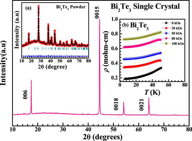
Figure 1 shows the single crystal XRD pattern of bulk Bi2Te3 indicating that the crystal is highly textured i.e. c- axis oriented showing all the diffraction peaks corresponding to the (00 l) reflections of the rhombohedral crystal structure with space group . The left inset of Fig. 1 represents the powder XRD pattern of bulk Bi2Te3 single crystal [Fig. 1(a)]. The lattice parameters found are a = b = 4.3866(2) Å and c = 30.4978(13)Å. The right inset of Fig. 1 displays the temperature dependence of electrical resistivity at different applied magnetic fields for the synthesized Bi2Te3 single crystal having a temperature range of 5 K to 50 K [Fig. 1(b)]. The applied magnetic field varies from 0 kOe to 100 kOe. Here, the value of resistivity increases with increase in temperature from 5 K to 50 K representing metallic behavior with and without applied magnetic field. Thus, the nature of this plot is in agreement to that observed in our earlier reported studies16. The extensive ongoing research activity worldwide on TIs inspired us to further explore the PL properties of bulk and few layers of Bi2Te3. As luminescent, insulators and semiconducting materials are widely studied, where PL originates from energy transfer from host to activator in the former and recombination of electron hole pair in the latter case. Energy transfer from insulators to conductors is also investigated in some composite systems17,18. Apart from composites, there isn’t any single material reported so far, where energy transfer from insulating to metallic states region takes place. It is well established that TIs are electronic materials having a bulk band gap like an ordinary insulator but have protected conducting states on their edges or surface. These states are protected by spin orbit interaction (SOI) and time reversal symmetry1. These striking features of TIs make it more interesting to explore their optical behavior particularly photoluminescence nature. Previous studies on 3D TIs showed existence of dual band gaps; 0.3 eV corresponding to electronic band gap and 2.1 to 2.3 eV corresponding to optical band gap for the case of CVD grown Bi2Se3 nanoplatelets14. The existence of optical band gap in these materials give rise to a strong PL which we have investigated on the basis of experimental and theoretical calculations. It is well-known that Bi2Te3 has a layered crystal structure which consists of five atomic layers blocks, known as quintuple layer (QL)16. Each QL contains five atomic layers ordered as Te-Bi-Te-Bi-Te. The bonding inside a QL is strong ionic-covalent type whereas QLs are separated by weak van der Waals forces1,2,8. The van der Waals gap in between the QLs makes Bi2Te3 cleavable as well as optically active.
Figure 1.

X-ray diffraction pattern for Bi2Te3 single crystal. Inset (a) shows the Rietveld fitted room temperature XRD pattern for powder Bi2Te3 crystal. (b) Temperature dependence of electrical resistivity at different magnetic fields for Bi2Te3 single crystal.
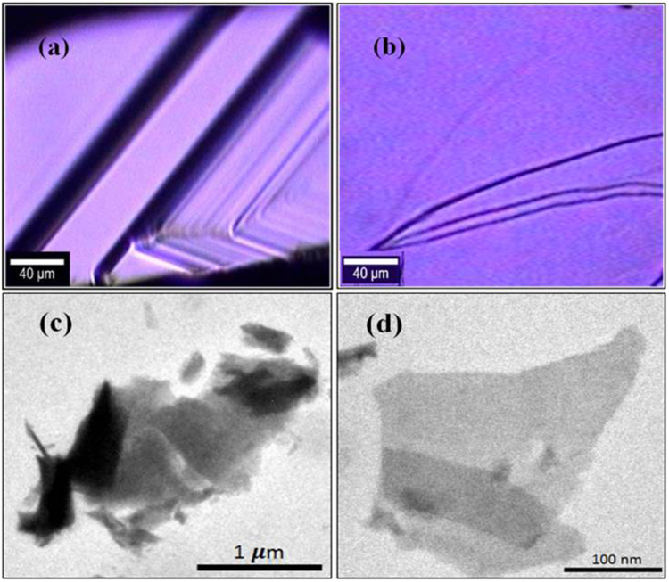
The PL measurements are done for both bulk Bi2Te3 single crystal as well as for mechanically exfoliated few layers of Bi2Te3. The optical images of both cases are shown in Fig. 2(a) and (b), respectively. The representative TEM images for bulk single crystal and few layers are shown in Fig. 2(c) and (d), respectively, which clearly differentiate between them. The SEM micrograph of Bi2Te3 as shown in Figure S1 (see Supplementary Information) clearly visualizes the layered structure. The TEM micrograph of bulk Bi2Te3 is shown in Figure S2 (see Supplementary Information) to further distinguish between bulk and exfoliated few layers Bi2Te3. The decrease in transparency is associated with increase in number of QLs. Further, well resolved lattice fringes obtained from HRTEM micrograph in Figure S3 (see Supplementary Information) shows the formation of Bi2Te3. The inter-planer spacing from the HRTEM micrograph comes out to be 0.21 nm. The SAED pattern with well indexed diffraction rings further confirms the lattice formation of Bi2Te3 as shown in Figure S4 (see Supplementary Information). Moreover, the atomic force microscopy (AFM) result confirms the thickness of mechanically exfoliated layers of Bi2Te3 is (18 ± 2) nm as shown in Figure S5.
Figure 2.
(a) Optical image of bulk Bi2Te3 single crystal. (b) Optical image of scotch tape taken few layers of Bi2Te3. (c) TEM image of bulk Bi2Te3 single crystal. (d) TEM image of few layers of Bi2Te3.
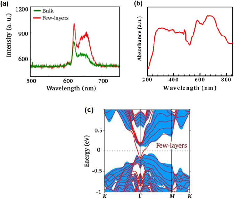
Angle resolved photoemission spectroscopy (ARPES) result shown in Figure S6 depicts energy distribution map (EDM) measured near the zone center for Bi2Te3 at a sample temperature of 20 K using 70 eV photon energy and p-polarized light. Dirac point is located at a binding energy of 300 meV below the Fermi level as shown by the green arrow on the EDM. The ARPES data is taken at Elettra synchrotron light source. This result clearly shows that the as synthesized Bi2Te3 single crystal is topological in nature because the band dispersion in the vicinity of the Fermi level as shown in Figure S6 is purely of the topological surface state (upper part of the Dirac cone) although the Dirac point is at around 300 meV below the Fermi level. However, there are several reports discussing the presence of bulk bands near the Fermi level that are generally induced by the crystal disorder19. Thus, the absence of bulk bands near the Fermi level in our system suggests a high quality of the crystal with minimum defects. Figure 3(a) shows the PL emission spectra of both bulk Bi2Te3 single crystal and mechanically exfoliated few layers of Bi2Te3 upon excitation at 375 nm marked in black and red color respectively. The emission spectrum of bulk Bi2Te3 single crystal shows a strong red emission at 621.32 nm (~2 eV). Also, several other closely spaced spectral peaks appears in the red region from ~ 630 nm to 700 nm. Similar peaks were also observed in the case of mechanically exfoliated few layers of Bi2Te3 in the same region. However, significant enhancement in PL intensity is observed in the case of few layers of Bi2Te3 because of the decreasing number of QL which induces the efficient photon emission from few layers of Bi2Te3 due to internal transitions taking place in the sub-levels of this system. Accordingly, the optical penetration loss effect depends on the sample thickness. The present experimentally observed PL emission centered about 2 eV differs from that observed in the range of 2.1–2.3 eV for Bi2Se3 in another study14. The obvious reason could the difference in two TI systems with different morphologies and dimensions having different inter band transitions which enable different optical band gaps.
Figure 3.
(a) PL spectrum of Bi2Te3 single crystal and mechanically exfoliated few layers. Green and red colors identify spectrum of bulk and few layers, respectively. (b) Absorbance spectrum of mechanically exfoliated few layers of Bi2Te3. (c) A few layers band structure of Bi2Te3 with the inclusion of spin-orbit coupling along high symmetry directions in the (001) surface Brillion zone. Note that we have taken 6 QLs in our calculations as a representative case for few layers Bi2Te3. The shaded part refers to the bulk states.
The few layers of Bi2Te3 are mechanically exfoliated from the bulk single crystal using the standard scotch – tape method20–22 and hence, their thickness is considerably reduced to few QLs in comparison to the bulk Bi2Te3 single crystal where efficient photon emission is possible without the major peak shift like other 2D materials. In our investigated systems (Bi2Te3), we expostulate and understand the enhancement in PL emission is due to the higher photon emission into the thin flake of Bi2Te3 via Fӧrster mechanism. More specifically, reduction of volume to surface area provides better photon energy emission due to internal transitions occurring in the sub-levels of the few layers of mechanically exfoliated Bi2Te3 without much of non-radiative loss like in the bulk system. Generally, PL may arise from such system due to defect or impurity present in crystal structure. The exact mechanism of the photon emission is however complex and requires further analysis. To further ensure the PL experiment and origin of PL, the absorbance analysis were performed to correlate with theoretical estimated data of mechanically exfoliated few layers of Bi2Te3. The reflectance spectrum of mechanically exfoliated few layers of Bi2Te3 is shown in Figure S7 (see Supplementary Information). Figure 3(b) depicts the absorbance spectrum of mechanically exfoliated few layers of Bi2Te3 calculated using the formula A = Log10 1/R, where A and R represents the absorbance and reflectance respectively. Here, we noticed strong absorption peaks at 576 nm and 663 nm which have good agreement with the observed PL peaks at 620 and 650 nm. Moreover, few more peaks are observed similar to the theoretical calculation of partial density of states (PDOS) [Fig. 4(a-b)]. In order to develop a better understanding of the underlying mechanism for observed PL, we employ density functional theory based calculations, using both the WIEN2k23 as well as VASP24 suite of codes. The generalized gradient approximation (GGA) is used to include exchange correlation effects25. Our calculations are performed with the inclusion of spin-orbit coupling (SOC). We have used 6 QLs to explicitly model few layers of Bi2Te3. The band structure of a few layers (6 QLs) of Bi2Te3 with the inclusion of SOC is displayed in Fig. 3(c) where the shaded part arises from the bulk. Our results show an insulating energy spectrum for bulk Bi2Te3 whereas its few layers have additional Dirac-cone-like conducting surface states inside the bulk energy gap. These results clearly demonstrate that Bi2Te3 is a topological insulator with different electronic states inside the bulk and on the surface and therefore, it is possible to have more photon emissions from such thin layers of Bi2Te3 due to the internal transitions of the sub-levels in the present TI system.
Figure 4.

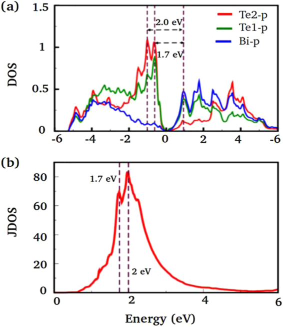
(a) Partial density of states (PDOS) and (b) Joint density of states (JDOS) for bulk Bi2Te3 with the inclusion of spin-orbit coupling. Te1 and Te2 in (a) represent Te atoms at the edge and the center of QL, respectively.
To further explore the energy levels electronic transitions responsible for PL emission, we show in Fig. 4(a-b) the partial density of states (PDOS) for bulk with the inclusion of SOC. It should be noted that PDOS of few layers of Bi2Te3 has significant change in comparison to the bulk, which is consistent with the experiments, except the appearance of small DOS at Fermi-level which is due to the presence of topological surface states. The PDOS profile clearly shows the existence of dominant electronic transitions between Te-p to Bi-p states. These electronic transitions have energies of ~1.7 eV and ~2 eV and are in substantial agreement with the observed PL peaks noted in Fig. 3(a). We have also found additional electronic transitions at higher energies and are not shown here as they lie away from the range of our measured PL spectra. Alternatively, we have calculated the joint density of states (JDOS) which does not have any broadening. The JDOS shown in Fig. 4(b) clearly identifies two dominant peaks at ~1.7 eV and ~2 eV, in qualitative agreement with our experimental observations except for the splitting size. This can be understood because of well known limitations of DFT in underestimating the gap. Hence a quantitative agreement with observed experimental is not possible.
Discussion
In conclusion, we report the optical band gap of bulk single crystals and mechanically exfoliated few layers of Bi2Te3 of around 2 eV, which is greater than its electronic band gap (~0.15 eV).This is consistent with our first-principles calculations. The experimentally observed 2 eV optical band gap in the visible region for bulk as well as for mechanically exfoliated few layers of Bi2Te3 clearly rules out the quantum confinement effects in the investigated samples which are the new paradigm shifts from other 2D systems like MoS2,WS2, WSe2, MoSe2etc for 1–3 layers. Our results provide a stepping stone for further exploration of topological insulators for next generation optoelectronic, photonic, and spintronics applications.
Methods
The synthesis of bulk Bi2Te3 single crystal used for this study were carried out by self-flux method via the solid state reaction route16. High purity (99.999%) Bismuth (Bi) and Telluride (Te) powders were accurately weighed according to the stoichiometric ratio of 2:3 and mixed thoroughly using mortar and pestle inside a glove box filled with argon gas. The homogeneous mixture was then pressed into a rectangular pellet with the help of hydraulic press (40 kg/cm2) and vacuum sealed (10−3 Torr) in a quartz tube. Further, the quartz tube was kept inside a tube furnace and heated to 950 °C (2 °C/min) for 12 hours. The furnace was then allowed to cool very slowly to 650 °C (1 °C/30 min) after which it was switched off. The resultant crystal obtained was shiny and silver in color.
Measurements and Characterizations
In order to investigate the phase structure of the synthesized sample X-ray diffraction (XRD) was performed using Rigaku X-ray diffractometer with Cu-Kα1 radiation (λ = 1.5418 Å). The temperature dependent resistivity measurements were carried out using a quantum design 14 Tesla Physical Property Measurement System (PPMS). The thickness of the few layers of mechanically exfoliated Bi2Te3 was investigated by atomic force microscope (AFM, Model no. NT-MDT Solver Scanning probe Microscope). The absorbance measurements were carried out using Avantes spectrometer with AvaLight-DH-S-BAL balanced power source. For PL measurements, mechanically exfoliated20,21 few layers of Bi2Te3were obtained using the standard scotch tape method22. However, the PL measurements were done using WITec alpha 300 R+ confocal PL microscope system using 375 nm diode laser as a source of excitation. In order to prevent the damage of bulk Bi2Te3 single crystal and few layers of Bi2Te3, caution was taken and the power setting for the excitation laser was maintained to lower values. Further, the surface morphology Transmission Electron Microscopy (TEM) was performed using Technai G20-twin operating at 200 kV.The ARPES data istaken at Elettra synchrotron light sourceat a sample temperature of 20 K using 70 eV photon energy and p-polarized light. In order to understand the measured PL spectrum we present density functional theory based calculations of the optical properties of Bi2Te3 for bulk and few layer structures.
Electronic supplementary material
Acknowledgements
Authors from CSIR-NPL would like to thank their Director NPL India for his keen interest in the present work. This work is financially supported by DAE-SRC outstanding investigator award scheme on search for new superconductors. Rabia Sultana thanks CSIR, India for research fellowship and AcSIR-NPL for Ph.D. registration. SA would like to thank the High Performance Computing (HPC) facilities at Intra-University Accelerator Centre (IUAC) at New Delhi, Indian Institute of Mathematical Sciences (IMSC) at Chennai, CSIR- 4PI at Bengaluru, University of Hyderabad (UoH) in Hyderabad and Physics Department Indian Institute of Technology at Kanpur.
Author Contributions
B.K.G. and V.P.S.A. conceived the concepts of the research. R.S., G.A. and A.G. designed and synthesized the samples as well as performed the resistivity vs temperature measurements. S.S. performed the AFM and PL measurements of sample. A.K.S. performed the transmission electron microscopy of the sample. V.S., B.S. and S.A. performed the theoretical analysis. B.K.G., V.P.S.A., R.S., O.N.S. and S.A. wrote the manuscript and analysed the data.
Competing Interests
The authors declare no competing interests.
Footnotes
Electronic supplementary material
Supplementary information accompanies this paper at 10.1038/s41598-018-27549-0.
Publisher's note: Springer Nature remains neutral with regard to jurisdictional claims in published maps and institutional affiliations.
Contributor Information
Bipin Kumar Gupta, Email: bipinbhu@yahoo.com.
V. P. S. Awana, Email: awana@nplindia.org
References
- 1.Hasan MZ, Kane CL. Colloquium: Topological insulators. Rev. Mod. Phys. 2010;82:3045–3067. doi: 10.1103/RevModPhys.82.3045. [DOI] [Google Scholar]
- 2.Ando Y, Fu L. Topological Crystalline Insulators and Topological Superconductors: From Concepts to Materials. Annu. Rev. Condens. Matter Phys. 2015;6:361–381. doi: 10.1146/annurev-conmatphys-031214-014501. [DOI] [Google Scholar]
- 3.Tang H, Liang D, Qiu RLJ, Gao XPA. Two-Dimensional Transport-Induced Linear Magneto-Resistance in Topological Insulator Bi2Se3 Nanoribbons. ACS Nano. 2011;5:7510–7516. doi: 10.1021/nn2024607. [DOI] [PubMed] [Google Scholar]
- 4.Zhang SX, et al. Magneto-resistance up to 60 Tesla in topological insulator Bi2Te3 thinfilms. Appl. Phys. Lett. 2012;101:202403–202406. doi: 10.1063/1.4766739. [DOI] [Google Scholar]
- 5.Ning W, et al. One-dimensional weak anti localization in single-crystal Bi2Te3 nanowires. Sci. Rep. 2013;3:1564–1569. doi: 10.1038/srep01564. [DOI] [PMC free article] [PubMed] [Google Scholar]
- 6.Fu L, Kane CL, Mele EJ. Topological Insulators in Three Dimensions. Phys. Rev. Lett. 2007;98:106803–106806. doi: 10.1103/PhysRevLett.98.106803. [DOI] [PubMed] [Google Scholar]
- 7.Moore JE, Balents L. Topological invariants of time-reversal-invariant band structures. Phys. Rev. 2007;B75:121306–121309. doi: 10.1103/PhysRevB.75.121306. [DOI] [Google Scholar]
- 8.Ando Y. Topological Insulator Materials. J. Phys. Soc. Jpn. 2013;82:102001–102032. doi: 10.7566/JPSJ.82.102001. [DOI] [Google Scholar]
- 9.Zhang J, et al. Raman Spectroscopy of Few-Quintuple Layer Topological Insulator Bi2Se3 Nanoplatelets. Nano Letters. 2011;11:2407–2414. doi: 10.1021/nl200773n. [DOI] [PubMed] [Google Scholar]
- 10.He L, et al. Surface-Dominated Conduction in a 6 nm thick Bi2Se3 Thin Film. Nano Lett. 2012;12:1486–1490. doi: 10.1021/nl204234j. [DOI] [PubMed] [Google Scholar]
- 11.Wang H, et al. Crossover between Weak Anti localization and Weak Localization of Bulk States in Ultrathin Bi2Se3 Films. Sci. Rep. 2014;4:5817–5822. doi: 10.1038/srep05817. [DOI] [PMC free article] [PubMed] [Google Scholar]
- 12.Checkelsky JG, Hor YS, Cava RJ, Ong NP. Bulk Band Gap and Surface State Conduction Observed in Voltage-Tuned Crystals of the Topological Insulator Bi2Se3. Phys. Rev. Lett. 2011;106:196801–196804. doi: 10.1103/PhysRevLett.106.196801. [DOI] [PubMed] [Google Scholar]
- 13.Zhao M, et al. Actively Tunable Visible Surface Plasmons in Bi2Te3 and their Energy-Harvesting Applications. Adv. Mater. 2016;28:3138–3144. doi: 10.1002/adma.201506367. [DOI] [PubMed] [Google Scholar]
- 14.Vargas A, Liu F, Kar S. Giant enhancement of light emission from nanoscale Bi2Se3. Appl. Phys. Lett. 2015;106:243107–243110. doi: 10.1063/1.4922729. [DOI] [Google Scholar]
- 15.Eda G, et al. Photoluminescence from Chemically Exfoliated MoS2. Nano Lett. 2011;11:5111–5116. doi: 10.1021/nl201874w. [DOI] [PubMed] [Google Scholar]
- 16.Sultana R, Neha P, Goyal R, Patnaik S, Awana VPS. Unusual non saturating Giant Magneto-resistance in single crystalline Bi2Te3 topological insulator. J. Magn. Mag. Mater. 2017;428:213–218. doi: 10.1016/j.jmmm.2016.12.011. [DOI] [Google Scholar]
- 17.Liu X, Lei DY. Simultaneous excitation and emission enhancements in upconversion luminescence using plasmonic double-resonant gold nanorods. Sci. Rep. 2015;5:15235–15246. doi: 10.1038/srep15235. [DOI] [PMC free article] [PubMed] [Google Scholar]
- 18.Fischer S, et al. Plasmon enhanced upconversion luminescence near gold nanoparticles–simulation and analysis of the interactions. Opt. Express. 2012;20:271–282. doi: 10.1364/OE.20.000271. [DOI] [PubMed] [Google Scholar]
- 19.Chen YL, et al. Experimental Realization of a Three Dimensional Topological Insulator, Bi2Te3. Science. 2009;325:178–181. doi: 10.1126/science.1173034. [DOI] [PubMed] [Google Scholar]
- 20.Cho S, Butch NP, Paglione J, Fuhrer MS. Insulating Behavior in Ultrathin Bismuth Selenide Field Effect Transistors. Nano Lett. 2011;11:1925–1927. doi: 10.1021/nl200017f. [DOI] [PubMed] [Google Scholar]
- 21.Hong SS, et al. Ultrathin Topological Insulator Bi2Se3Nanoribbons Exfoliated by Atomic Force Microscopy. Nano Lett. 2010;10:3118–3122. doi: 10.1021/nl101884h. [DOI] [PubMed] [Google Scholar]
- 22.Liao ZM, et al. Surface plasmon on topological insulator/dielectric interface enhanced ZnO ultraviolet photoluminescence. AIP Advances. 2012;2:022105. doi: 10.1063/1.3703320. [DOI] [Google Scholar]
- 23.Blaha, P., Schwarz, K., Madsen, G., Kvasnicka, D. & Luitz, J. WIEN2K, An Augmented Plane Wave + Local Orbitals Program for Calculating Crystal Properties K. Schwarz, Tech. Univ. Wien, Austria (2001).
- 24.Kresse G, Furthm̈uller J. Efficient iterative schemes for ab initio total-energy calculations using a plane-wave basis set. Phys. Rev. 1996;B54:11169–11186. doi: 10.1103/PhysRevB.54.11169. [DOI] [PubMed] [Google Scholar]
- 25.Perdew JP, Burke K, Ernzerhof M. Generalized Gradient Approximation Made Simple. Phys. Rev. Lett. 1996;77:3865–3868. doi: 10.1103/PhysRevLett.77.3865. [DOI] [PubMed] [Google Scholar]
Associated Data
This section collects any data citations, data availability statements, or supplementary materials included in this article.


