Abstract
A supply-doubled pulse-shaping high voltage (HV) pulser is presented for medical ultrasound imaging applications, particularly those that use capacitive micromachined ultrasonic transducers (CMUT). The pulser employs a bootstrap circuit combined with dynamically-biased stacked transistors, which allow HV operation above process limit without lowering device reliability. The new pulser overcomes supply voltage limitation of conventional unipolar pulsers by generating output signals that are almost twice the supply level. It also can generate three-level pulses to further optimize the transmit pressure signals. A proof-of-concept prototype has been implemented in 0.18-μm HV CMOS/DMOS technology with 60 V devices. Measurement results show that the HV pulser can safely generate controllable three-level pulses with up to 85 Vpp from 45 V supply. Acoustic measurements are conducted connecting the pulser to a CMUT with 2 pF capacitance and 8.3 MHz center frequency. The pulse shape has been adjusted for the CMUT under test to generate maximum pressure output and the results are in good agreement with a large signal CMUT model.
Index Terms: High voltage pulser, capacitive micromachined ultrasound transducer (CMUT), medical ultrasound imaging
I. Introduction
Medical ultrasound imaging has had a significant impact on clinical practice by providing real-time images of different organs with high spatiotemporal resolution non-invasively at low cost [1]. In recent years, the capacitive micromachined ultrasound transducers (CMUT) have shown several advantages over the conventional bulk piezoelectric transducers, due to smaller size, wider bandwidth, and ease of integration with interfacing circuitry [2]. Compared to piezoelectric transducers, CMUTs typically have larger electrical impedances for the same transducer area. Although integration with reduced parasitics lead to low noise CMUT receivers [3], larger voltages are required to generate the required pressure output by CMUT transmitters as compared to piezoelectric transducers. Therefore, CMUT based ultrasound systems would benefit from high voltage (HV) ultrasound pulse generators that utilize the maximum available voltage level given the integrated circuit process constraints.
Ultrasound pulse generator, aka pulser, is one of the key building blocks of medical ultrasound imaging systems, which drives the ultrasound transducers, including CMUTs with high voltage (HV) output swing to create an ultrasonic pressure pulse towards the target tissue. HV digital pulsers are commonly used in current commercial systems for their simplicity [4], while recent publications shows that linear amplifiers are also becoming attractive in driving piezoelectric transducers, capable of generating low harmonic content signals by adopting apodization profiles [5]. To drive a CMUT load, however, its nonlinear distortion could refute good linearity performance of the linear amplifier’s output signal. Moreover, amplifiers have higher power consumption and considerable power loss when charging and discharging the CMUT parasitic capacitance, which reduce the pulser power efficiency [6]. A three-level pulser with pulse shaping and charge recycling capabilities has also been reported in [7], saving power in the pulser at the cost of requiring multiple supply voltages, which need HV DC-DC converters and extra capacitors, which increase the overall system complexity and power consumption. Furthermore, there is demand for pulsers capable of generating versatile HV output waveforms efficiently within a compact chip area especially for applications such as intracardiac echocardiography (ICE) and intravascular ultrasound (IVUS) imaging, which are implemented on catheters that are only 1 mm to 3.3 mm in diameter (3–10 F) [8].
The main challenges in designing interface electronics in these applications are limited space, temperature rise, supply voltage drop across long interconnects, and number of control lines in the catheter. These applications clearly benefit from interface electronics integration, such as CMUT-on-CMOS or flip-chip bonding [9], [10]. To further reduce the catheter electrical interconnect complexity, the ultrasonic transmitter (US-Tx) beam-forming, driver electronics and HV pulser can be integrated directly under the CMUT array. In addition, the CMUT fabrication processes allow for fabricating HV capacitors within its MEMS structure, which can be used in the pulser bootstrap circuit to further reduce the size and voltage drop across the long catheter wires by using a lower external supply voltage.
In this brief, we present an integrated HV pulser for CMUT arrays, that provides pulse-shaping and an output swing close to twice its supply voltage above the device breakdown, which is often limited by the CMOS process. The following section describes the new pulser circuit topology, including its voltage doubler. Experimental setup with CMUT and measurement results are presented in section III, followed by conclusions.
II. High Voltage Pulser Design
A. Circuit topology
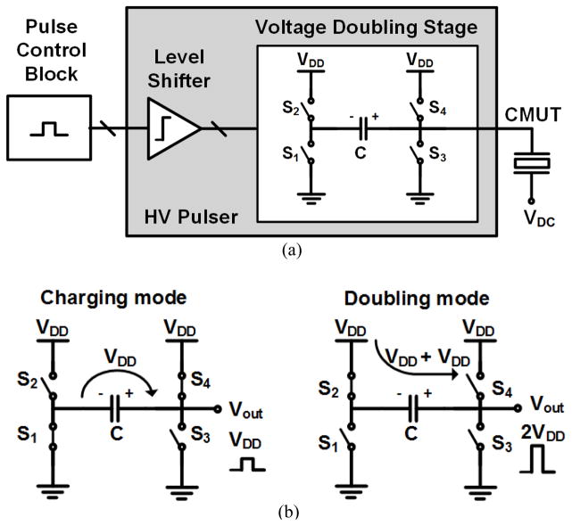
The primary objective of this circuit is to generate sharp pulses with amplitudes close to twice the supply voltage without violating safe operating range of its circuit elements. A simplified schematic diagram of the proposed pulser is depicted in Fig. 1a. The external control logic generates low voltage control signals and level shifters convert the dc voltage levels to drive double-diffused metal oxide semiconductor (DMOS) transistors of the pulser. Fig. 1b shows operation of the voltage doubling stage. A capacitor, C, which can be on-chip or integrated with the CMUT array, is charged to VDD during charging mode through S1 and S4. Then, a HV switch, S2, drives the negative terminal of C to VDD during doubling mode, while all other switches are open for Vout to reach 2VDD. S3 is used to discharge C by connecting it to ground. The CMUT can be modeled mainly as a capacitive load, resulting in a capacitive voltage divider between C and CMUT, which indicates the actual output pulse voltage. The voltage doubling stage requires careful design because it goes beyond the process operating voltage. To ensure safe operation, we employed dynamically gate-biased transistor stack and Schottky diodes to protect all the transistors from out of range operating conditions.
Fig. 1.
(a) Simplified schematic diagram of the supply-doubled pulse-shaping high voltage pulser, and (b) the operation of voltage doubling stage.
B. Design and operation of voltage-doubling pulser
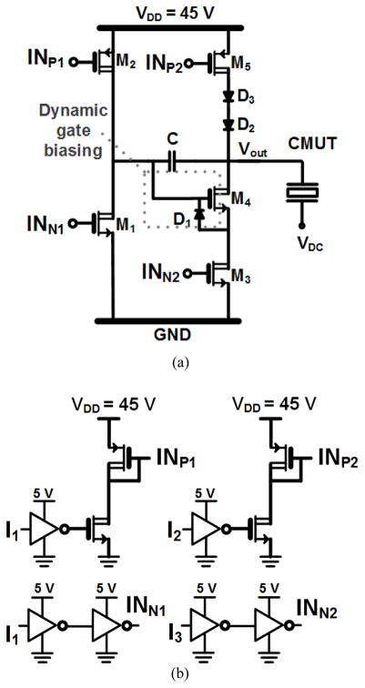
Fig. 2 shows detailed schematic of the proposed pulser, which is driven by three input control signals (I1, I2, and I3). Two N-type DMOS transistors, M1 and M3, are driven by 0 – 5 V control signals. Two P-type DMOS transistors, M2 and M5, are driven by 40 – 45 V level-shifted control signals. Note that in this case, VDD = 45 V. To achieve a compact design, simple level shifters are used in Fig. 2b, while ensuring that INP1 and INP2 generate 40–45 V sharp pulses with low current consumption, compared to the CMUT driving stage [11].
Fig. 2.
(a) Schematic of the proposed voltage doubled pulser. (b) Schematic of the input driving buffers and level shifters for high voltage PMOS input signals.
The circuit operation is similar to the bootstrapping circuits in [12]. During charging mode, the external capacitor, C, is charged up to VDD − (VD2 + VD3) by turning on M1 and M5 transistors, where (VD2 + VD3) is the forward voltage drop across D2 and D3. When C is charged, we turn on M2 and turn off all the other transistors so that Vout is bootstrapped to 2VDD − (VD2 + VD3). During this doubling mode, it is crucial to ensure that all devices in the circuit are operated in their safe operating conditions, considering the fact that in this process, the drain-source junction breakdown and gate-oxide breakdown voltages are 60 V and 5 V, respectively. To prevent excessive VDS on M5 and its parasitic N-well substrate diodes from turning on, two HV Schottky diodes are added in series with M5. Each diode has a maximum reverse voltage of 36 V, and when the output is doubled, the two diodes should handle 45 V of total reverse voltage between them, resulting in each diode having reverse voltage well below its limit.
Between Vout terminal and GND, stacked N-type DMOS transistors, M3 and M4, are used to ensure safe operation when Vout is doubled. The gate of M4 is dynamically biased to VDD during doubling mode, while M3 is turned off. The Zener diode, D1, keeps VGS of M4 below 5 V, so that M3 and M4 can divide the doubled output voltage across their designated drain-source voltage limit.
The value of external capacitor, C, is key to determine the pulser Vout and slew rate according to,
| (1) |
| (2) |
where CCMUT is the equivalent capacitance of the CMUT. Therefore, C should be large to obtain higher Vout. However, larger C would increase the output RC time constant, limiting the operating frequency range and slew rate of output pulses,
| (3) |
where Imax is the maximum current sourced to capacitance. By decreasing slew rate, Vout will suffer from slow charging problem. Moreover, if C is integrated in the CMUT, its value may be limited by the size of the CMUT. Thus deciding the optimal value of C is critical in the pulser design.
In this study, we consider a particular application of 2-D CMUT array for intracardiac echography (ICE), where the center frequency is about 8.3 MHz and CMUT array element size is limited to approximately 100 × 100 μm2, resulting in CCMUT = 2 pF. We also investigated the case for an 8 pF device capacitance, realized by an oscilloscope probe (P6139A, Tektronix) in electrical characterization.
A realistic design target for the pulser would be to achieve peak HV level of at least 1.8 × VDD while having a rise time less than a quarter period of the CMUT center frequency, i.e. 30 ns for the 8.3 MHz CMUT. (1) and (2) suggest that the minimum required C would be > 4 × CCMUT. Considering the forward voltage drop across the diodes and parasitic capacitances of the large DMOS transistors, we chose C = 30 pF for 2 pF of CCMUT. Also to obtain SR > 3 V/ns during the charging mode, we designed M5 to have Imax > 100 mA, based on (3). Since the size of large DMOS transistors mainly define the layout size, we chose Imax for driving a 2 pF CMUT load at 8.3 MHz center operating frequency.
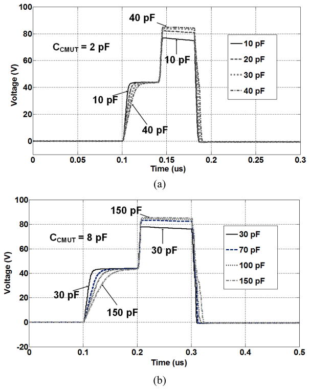
To verify the pulser design and compare with measurements we simulated the voltage-doubled output pulse for 2 pF of CMUT load and 8 pF of passive probe loading, for which C was changed within 10 – 40 pF and 30 – 150 pF, respectively. For ensuring the initial condition of Vout = 0 V, a 100 kΩ resistor was added in parallel with C, which adds a slight slope on doubled output pulse with minimal effect on output voltage division. With 2 pF load, C = 30 pF shows 85 Vpp of output pulse, rise time of 11.5 ns, and SR = 3.2 V/ns in the charging mode, which is suitable for driving a CMUT array with 8.3 MHz center frequency. With 8 pF load, C = 100 pF shows 85 Vpp of output pulse, rising time of 34.8 ns, and SR = 1.0 V/ns during charging mode. The slew rate of the doubling stage does not depend on the value of C, as evident in Fig. 3, because the charged C is simply connected in series with VDD.
Fig. 3.
Simulation of the output pulse with different C values, (a) when CMUT loading is considered 2 pF, (b) CCMUT = 8 pF.
C. Three level pulse shaping above the process limit
Multi-level pulsing circuits have been adopted in the past for driving CMUTs and piezoelectric transducers due to better power efficiency, requiring several supply voltages or DC-DC converters with large off-chip capacitors [7]. Since the capacitors required for DC-DC converters are often quite large, using off-chip components would be inevitable. A potential advantage of the proposed pulser is that it requires a capacitor 10 to 15 times larger than CCMUT, which can be implemented together with the CMUT microfabrication. For example, using a high-K dielectric like hafnium dioxide with er = 16, one can fabricate a capacitor with C > 10×CCMUT underneath the CMUT using the same area by replacing the vacuum gap with the high-K dielectric [12]. This approach would enable fabrication of a high voltage capacitor in the CMUT layer for compact ultrasound analog front end design.
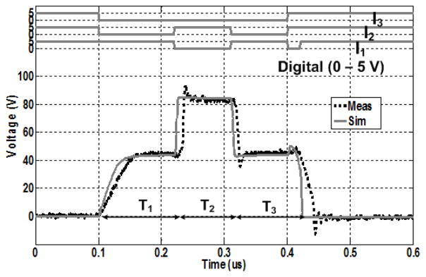
It is worth noting that this pulser surpasses the maximum operating voltage level imposed by the process to generate three different output levels. As shown in Fig. 4, with three control signals, I1, I2, and I3, the measurement results show that the pulser can generate up to 85 Vpp from 45 V supply. Different pulse shapes can be obtained with the three control signals. Changing durations of T1, T2, and T3 will affect the width of middle (45 V) and high (85 V) levels. Different pulse shapes affect the acoustic power and frequency content of the US-Tx, and there is an optimal pulse shape for maximizing the Tx acoustic power for any particular CMUT load.
Fig. 4.
Simulated and measured three-level output pulse along with three input control signals. C = 100 pF, CCMUT = 8 pF.
III. Experimental Results
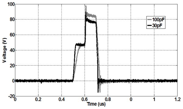
The proposed pulser was designed and fabricated in a 0.18-μm 60 V power management 4M1P HV-CMOS process, and occupied a core area of 0.2 mm2, as shown in Fig. 5. The chip was mounted on a PCB inside a QFN package along with an off-chip surface mount capacitor, C. Fig. 6 shows the measured output voltage with two different C and more than 8 pF loading, including the input capacitance of a passive probe and parasitic capacitance of wire-bonding and PCB routing in parallel with 100 kΩ resistor. The measured waveform with C = 100 pF, shows peak Vout = 85 V and slew rates of 0.88 V/ns, 3.2 V/ns, and 2.44 V/ns during charging, doubling, and falling modes, respectively. Similarly, with C = 30 pF, peak Vout = 78.6 V was achieved with slew rates of 2.1 V/ns, 2.9 V/ns, and 4.7 V/ns, respectively. Fig. 4 shows a sample measurement with non-zero T1, T2, and T3 values overlapped for comparison with the simulations.
Fig. 5.
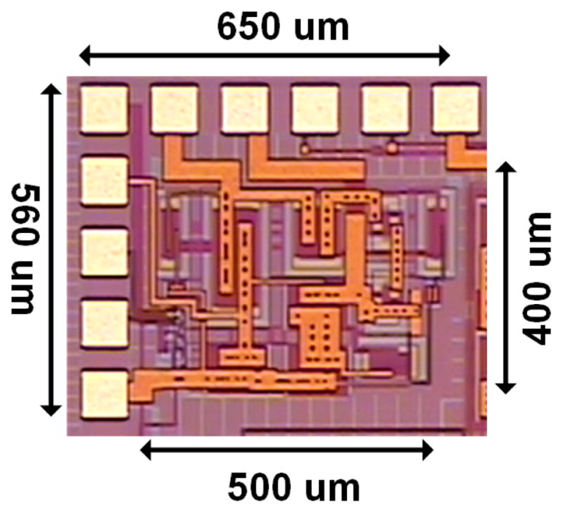
Microphotograph of the proposed pulser chip.
Fig. 6.
Measured output pulse with C = 30 pF and 100 pF when CMUT loading is 8 pF.
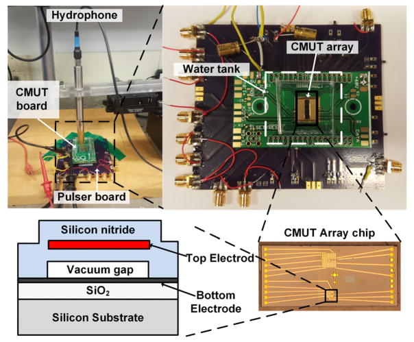
An acoustic pressure measurement setup was used to measure the US-Tx pressure with an actual CMUT load, as shown in Fig. 7. The CMUT used in this experiment occupied 100 × 100 μm2 area on silicon and consisted of a 2 × 2 array of four 45 μm wide square membranes. It created a 2 pF element, ~1.8 pF of which was due to bond pads parasitic capacitance, with 8.33 MHz center frequency and −3 dB bandwidth of 5 MHz. It was part of a larger 2-D ICE imaging array, which was fabricated using a low temperature CMOS-compatible process [9]. The CMUT array, mounted on a separate PCB, was connected to the larger pulser board via header pins. The off-chip capacitor, C = 30 pF, was selected to obtain maximum output swing and fast slew rate as discussed in section II. The CMUT array was submerged in a water tank, while a hydrophone (HGL-0085, Onda Corp) was placed above the CMUT array, 4.5 mm from its surface, to measure the US-Tx acoustic pressure. The pulser generates a single pulse with 60 ns pulse width and 8.3 MHz center frequency. We generated different pulse shapes to evaluate their impact on the US-Tx output pressure.
Fig. 7.
Acoustic pressure experimental setup with CMUT array board and pulser board.
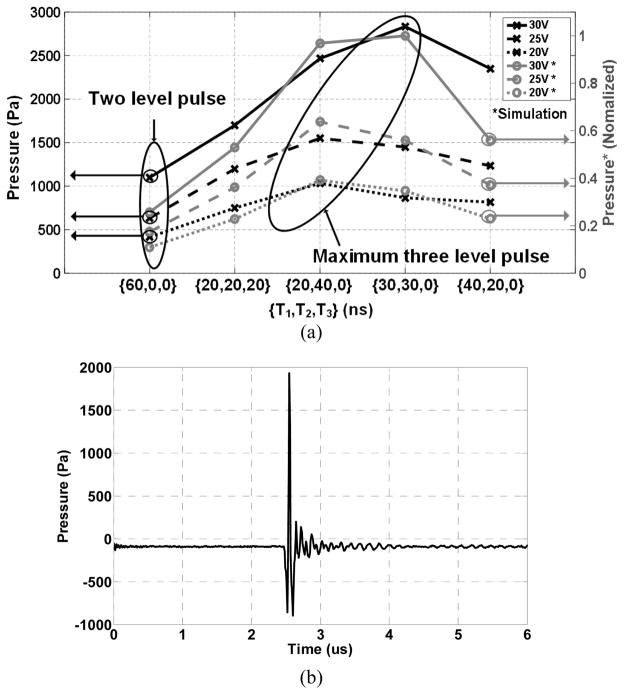
The pulse shape is defined by {T1, T2, T3}, as shown in the Fig. 4. When {T1, 0 ns, 0 ns} is applied, a two-level pulse is generated, which is not doubled. When only T3 is 0 ns, a three-level voltage doubled pulse, shown in Fig. 6, is generated. The measured peak-to-peak US-Tx pressure results are summarized in Fig. 8a. VDD in these experiments was reduced to 30 V because the CMUT breakdown voltage was 60 V. The maximum peak-to-peak pressure of 2467 Pa was recorded with {30, 30, 0}, as shown in Fig. 8b. This is a desired pulse shape because it generates more than twice the pressure level obtained from the conventional two-level pulse (1100 Pa) using the same 30 V supply. The optimal pulse shape varies with supply voltage because slew rate limitation can lower the maximum voltage level, reducing the acoustic output pressure. Pulses with T1 lower than the output RC settling time cannot fully double the supply voltage. Measured RC settling time showed 25 ns, hence 20 ns of T1 pulses might not efficiently generate supply doubled pulse with 30 V supply voltage, as shown in Fig. 8a. Measurements show that every doubled pulse shape generates higher pressure than the conventional two-level pulse. To test the validity of experimental results, we used a large signal nonlinear CMUT model to predict the pressure signal variations with similar pulse shapes [15]. Normalized pressure variations simulated by the model follow the measurements closely in Fig. 8a, indicating that this pulser structure along with the large signal model can offer higher performance. Table I summarizes the pulser specs for the {30, 30, 0} pulse shape and benchmarks its performance against prior work. Measurements from over 20 chips have shown consistent results with the maximum Vout (mean±std) = 84.24 ± 1.52 V, indicating reliability of this HV pulser circuit.
Fig. 8.
(a) Transmitted peak-to-peak acoustic pressure measurement and simulation with different pulse shapes and supply voltages. (b) Measured transmitted pressure with T1 = 30 ns, T2 = 30 ns, T3 = 0 ns, and VDD = 30 V.
Table I.
Benchmarking of the Proposed Pulser Performance
| Parameter | This work | [7] | [11] | [14] |
|---|---|---|---|---|
| Input voltage (V) | 5 | 3.3 | 3.3 | 1.8 |
| Output voltage (V) | 85 | 30 | 60 | 12.8 |
| VDD (V) | 45 | 30 | 60 | 12.8 |
| Frequency (MHz) | 8.33 | 2.5 to 5 | 1.38 | 1.25 |
| Rise/fall time (ns) | 26,16/18 | 30 | 68/68 | 40/50 |
| Power (mW) | 48.6 | 52.4 | 98.1 | |
| Power (mA) | 150 Dynamic * | - | - | 19.9 Dynamic * |
| Chip area (mm2) | 0.2 | - | 0.08 | 0.022 |
| Output load (pF) | 2 | 40 | 18 | 15 |
| Pulse shaping | Y | Y | N | N |
| Technology (μm) | 0.18 | 0.18 | 0.35 | 0.18 |
Simulation results
IV. Conclusions
This brief presents an integrated voltage-doubling and pulse-shaping HV pulser circuit to interface CMUT ultrasound systems in a 0.18-μm 60 V 4M1P CMOS/DMOS process. The presented circuit overcomes process limitation by adopting HV protection techniques that generate 85 Vpp of output pulse with 45 V supply voltage. A three level pulsing scheme is successfully applied to a CMUT array element and optimized for maximum acoustic pressure, as predicted by a large signal CMUT model, paving the way for simulation-based CMUT pulser optimization. The prototype pulser ASIC measurements were conducted with an off-chip capacitor, which can be integrated with the CMUT using high-K dielectric layers during CMUT fabrication. Our ongoing research involves co-optimization of the pulser and CMUT arrays using CMUT-on-CMOS technology for very compact catheter-based ultrasound imaging systems.
Acknowledgments
This work was supported in part by the National Institutes of Health under grants EB015607 and HL121838.
Contributor Information
Gwangrok Jung, GT-Bionics lab, School of Electrical and Computer Engineering at the Georgia Institute of Technology, Atlanta, GA 30308, USA.
Coskun Tekes, School of Mechanical Engineering at the Georgia Institute of Technology, Atlanta, GA 30332, USA.
Amirabbas Pirouz, School of Mechanical Engineering at the Georgia Institute of Technology, Atlanta, GA 30332, USA.
F. Levent Degertekin, School of Mechanical Engineering at the Georgia Institute of Technology, Atlanta, GA 30332, USA.
Maysam Ghovanloo, GT-Bionics lab, School of Electrical and Computer Engineering at the Georgia Institute of Technology, Atlanta, GA 30308, USA.
References
- 1.McDicken WN. Diagnostic Ultrasonics: Principales and Use of Instruments. New York: Wiley; 1997. p. 381. [Google Scholar]
- 2.Khuri-Yakub BT, Oralkan O. Capacitive micromachined ultrasound transducers for medical imaging and therapy. J Micromech Microeng. 2011 May;21(5):054004. doi: 10.1088/0960-1317/21/5/054004. [DOI] [PMC free article] [PubMed] [Google Scholar]
- 3.Gurun G, Hasler P, Degertekin F. Front-end receiver electronics for high-frequency monolithic CMUT-on-CMOS imaging arrays. IEEE Trans Ultrason Ferroelectr Freq Control. 2011 Aug;58:1658–1668. doi: 10.1109/TUFFC.2011.1993. [DOI] [PMC free article] [PubMed] [Google Scholar]
- 4.Wygant IO, Jamal NS, Lee HJ, Nikoozadeh A, Orlkan O, Karaman M, Khuri-Yakub BT. An integrated circuit with transmit beamforming flip-chip bonded to a 2-D CMUT array for 3-D ultrasound imaging. IEEE Trans Ultrason, Ferroelectr, Freq Control. 2009 Oct;56(10):2145–2156. doi: 10.1109/TUFFC.2009.1297. [DOI] [PubMed] [Google Scholar]
- 5.Bianchi D, Quaglia F, Mazzanti A, Svelto F. Analysis and design of a high voltage integrated class-B amplifier for ultra-sound transducers. IEEE Trans Circuits Syst I, Reg Papers. 2014 Jul;61(7):1942–1951. [Google Scholar]
- 6.Satir S, Degertekin FL. Harmonic reduction in capacitive micromachined ultrasonic transducers by gap feedback linearization. IEEE Trans Ultrason, Ferroelectr, Freq Control. 2012 Jan;59(1):50–59. doi: 10.1109/TUFFC.2012.2155. [DOI] [PMC free article] [PubMed] [Google Scholar]
- 7.Chen K, Lee H-S, Chandrakasan AP, Sodini CG. Ultrasonic imaging transceiver design for CMUT: A three-level 30-Vpp pulse-shaping pulser with improved efficiency and a noise-optimized receiver. IEEE J Solid-State Circuits. 2013 Nov;48(11):2734–2745. [Google Scholar]
- 8.Wong PC, Miller-Hance WC. Transesophageal Echocardiography for Congenital Heart Disease. London: Springer; 2014. Instrumentation for transesophageal echocardiography; p. 62. [Google Scholar]
- 9.Zahorian J, Hochman M, Xu T, Satir S, Gurun G, Karaman M, et al. Monolithic CMUT-on-CMOS integration for intravascular ultrasound applications. IEEE Trans Ultrason, Ferroelectr, Freq Control. 2011 Dec;58(12):2659–2667. doi: 10.1109/TUFFC.2011.2128. [DOI] [PMC free article] [PubMed] [Google Scholar]
- 10.Gurun G, Tekes C, Zahorian J, Xu T, Satir S, Karaman M, Hasler J, Degertekin FL. Single-chip CMUT-on-CMOS frontend system for real-time volumetric IVUS and ICE imaging. IEEE Trans Ultrason Ferroelectr Freq Control. 2014;61(2):239–250. doi: 10.1109/TUFFC.2014.6722610. [DOI] [PMC free article] [PubMed] [Google Scholar]
- 11.Behnamfar P, Molavi R, Mirabbasi S. Transceiver design for CMUT-based super-resolution ultrasound imaging. IEEE Trans Biomed Circuits Syst. 2016 Apr;10(2) doi: 10.1109/TBCAS.2015.2406777. [DOI] [PubMed] [Google Scholar]
- 12.Shikata A, Sekimoto R, Ishikuro H. A 0.5V 65nm-CMOS single phase clocked bootstrapped switch with rise time accelerator. IEEE Asia Pacific Conf. Circuits Syst; Dec. 2010.pp. 1015–1018. [Google Scholar]
- 13.Xu T, Tekes C, Degertekin F. CMUTs with high-K atomic layer deposition dielectric material insulation layer. IEEE Trans Ultrason, Ferroelect, Freq Contr. 2014 Dec;61(12):2121–31. doi: 10.1109/TUFFC.2014.006481. [DOI] [PMC free article] [PubMed] [Google Scholar]
- 14.Cha HK, Zhao D, Cheong JH, Guo B, Yu H, Je M. A CMOS high-voltage transmitter IC for ultrasound medical imaging applications. IEEE Trans Circuits Syst II, Exp Briefs. 2013 Jun;60(6):316–320. [Google Scholar]
- 15.Satir S, Zahorian J, Degertekin FL. A large-signal model for CMUT arrays with arbitrary membrane geometry operating in non-collapsed mode. IEEE Trans Ultrason Ferroelectr Freq Control. 2013;60(11):2426–2439. doi: 10.1109/TUFFC.2013.6644745. [DOI] [PMC free article] [PubMed] [Google Scholar]


