

Abstract
Motivated by recent progress in epitaxial growth of proximity structures of s-wave superconductors (S) and spin-active materials (M), in this paper we show that certain periodic structures of S and M can behave effectively as superconductors with pairs of point nodes, near which the low-energy excitations are Weyl fermions. A simple model, where M is described by a Kronig–Penney potential with both spin–orbit coupling and exchange field, is proposed and solved to obtain the phase diagram of the nodal structure, the spin texture of the Weyl fermions, as well as the zero-energy surface states in the form of open Fermi lines (Fermi arcs). As a second example, a lattice model with alternating layers of S and magnetic Z2 topological insulators is solved. The calculated spectrum confirms previous predictions of Weyl nodes based on the tunnelling Hamiltonian of Dirac electrons. Our results provide further evidence that periodic structures of S and M are well suited for engineering gapless topological superconductors.
This article is part of the theme issue ‘Andreev bound states’.
Keywords: superconductors, magnetic material, Weyl fermions, Andreev-bound states, superlattice, topological insulator
1. Introduction
The time-honoured recipe for discovering new super-conductors with interesting pairing symmetries or topological properties is via the synthesis of new materials. In recent years, an alternative approach has been advocated and gained experimental success. It is based on making proximity structures of s-wave superconductors (S) and spin-active materials (M) such as semiconductors, topological insulators [1,2] or ferromagnets with spin–orbit and/or exchange coupling. With proper design, the proximity structure can behave effectively as a superconductor with the desired symmetry or topology at energies below the bulk superconducting gap of S. For example, Fu & Kane [3] showed that the interface of a three-dimensional topological band insulator (TI) and an s-wave superconductor is analogous to a spinless px+ipy superconductor that hosts Majorana zero modes at vortex cores, as in two-dimensional superfluid 3He-A [4], or layered material Sr2RuO4 [5]. Similar states also arise in proximity structures of S and two-dimensional electron gas with Rashba spin–orbit coupling and Zeeman splitting either due to a nearby ferromagnetic insulator or an external magnetic field [6–10]. In one dimension, for example, a semiconductor nanowire [11] or a chain of ferromagnetic atoms deposited on a superconductor [12], Majorana zero modes are predicted to form at the sample edges. While it remains a challenge to fabricate and control the interface properties, or detect the unequivocal experimental signatures of these states, significant experimental progress has been made in recent years (for an overview, see [13,14]).
In this paper, we explore the possibility of realizing gapless topological superconductivity in S–M proximity structures in three dimensions. Specifically, we focus on superconducting states with topologically protected point nodes, i.e. the analogues of the A phase of superfluid 3He [4] and Weyl semimetals [15–17]. Such a state was predicted to appear in the superlattice structures of superconductors and magnetic topological insulators by Meng and Balents, and referred to as ‘Weyl superconductors’ [18]. The elegant analysis of Meng & Balents [18] is based on an effective Hamiltonian describing the tunnelling of the helical Dirac electrons (the surface states of TI) across the layers of TI and S, where the presence of the superconducting pairing potential and Zeeman field provide a mass to the Dirac electrons. The proposal of Meng and Balents can be viewed as the generalization of the earlier work on Weyl semimetals in the multilayer structures of trivial insulators and magnetic topological insulators [19]. One is then led to the following questions: Is it feasible to realize Weyl superconductors using materials other than topological insulators? Is the helical Dirac electron essential?
We answer these questions by considering a simple, idealized model of the S–M superlattice in §2. Here M stands for a general spin-active material with both spin–orbit coupling and exchange splitting (i.e. both the time reversal and spatial inversion symmetry are broken). We assume, as in [18], that the M layer is sufficiently thin so that the suppression of superconductivity is not significant and the superconducting phase coherence is maintained across the M layers. This motivates us to approximate the M layers as delta function spin-active potentials, similar to the well-known Kronig–Penney model. In §3, the band structure of this model is solved to illustrate the reconstruction of the low-energy spectrum due to the periodic spin-active potential, the pseudo-spin texture of the corresponding eigenstates are shown and the low-energy effective Hamiltonians near the Weyl nodes are discussed. In §4, zero-energy surface states that manifest the non-trivial topological properties of the superconducting state, usually referred to as Fermi arcs [20], are discussed. We identify parameter regimes where the spectrum has one pair or two pairs of Weyl nodes and present the phase diagram of this model in §5. This model clearly illustrates that neither TI nor helical Dirac electrons are necessary for Weyl nodes to appear in S–M superlattices.
To provide an alternative description of the S–M superlattice and estimate the design parameters for Weyl superconductors, we move to study TI–S periodic structures using tight-binding lattice models in the rest of this paper. However, in contrast to Meng & Balents [18], we start from microscopic models of S and TI instead of an effective model based on the low-energy surface degrees of freedom. We present the microscopic lattice model for the S–TI superlattice in §6, in which each unit cell consists of a few layers of S and another few layers of magnetized TI with a tunable hopping matrix describing the coupling between the two materials, and outline a procedure to compute the energy spectrum of the superlattice. In §7, we briefly review the properties of a single S–TI interface [3], and discuss the relation between the Andreev-bound states (ABS) at a single interface [21] and the spectrum of multilayer systems. In §8, we assess the requirements to realize Weyl superconductors with one pair of nodes and two pairs of nodes, respectively. Finally, we present our conclusions in §9.
2. A simple model for the S–M superlattice
We consider a periodic layered structure of an s-wave superconductor (S) and a spin-active material (M) extending in the z-direction as schematically shown in figure 1. As far as the low-energy excitations are concerned (relative to the bulk superconducting gap Δ), M amounts to a periodic spin-active potential  , where the hat denotes matrices in spin space. To preserve the superconductivity throughout the whole structure, the M layers should not be too thick, so we assume the M layer thickness is much smaller than the period d. In this limit,
  can be modelled by Kronig–Penney potential of the form
| 2.1 |
Here,  ’s are the Pauli matrices in the spin space, and k∥=(kx,ky) is the transverse momentum which is conserved due to translational invariance on the xy-plane. Note that the material details of M do not enter into this description, they are encoded in V
0 and V
i which are chosen to reproduce the scattering matrix of electrons by M. The superlattice is then described by the following Hamiltonian in the particle-hole space,
’s are the Pauli matrices in the spin space, and k∥=(kx,ky) is the transverse momentum which is conserved due to translational invariance on the xy-plane. Note that the material details of M do not enter into this description, they are encoded in V
0 and V
i which are chosen to reproduce the scattering matrix of electrons by M. The superlattice is then described by the following Hamiltonian in the particle-hole space,
 |
2.2 |
with  ; the check denotes a matrix in the particle-hole and spin space. Note that we have assumed Δ to be homogeneous, and for z=nd (i.e. inside M), the potential
  dominates all other terms in the Hamiltonian. For simplicity, we shall put V
0=0. To model M with both spin–orbit coupling and exchange splitting, we assume that
dominates all other terms in the Hamiltonian. For simplicity, we shall put V
0=0. To model M with both spin–orbit coupling and exchange splitting, we assume that  takes the form [22]
| 2.3 |
where vso is the strength of Rashba spin–orbit coupling, and vz is the Zeeman (exchange) field along the z-direction. Using the periodicity of the Hamiltonian,  , the band structure can be easily obtained by the expansion of the wave function via Bloch’s theorem
| 2.4 |
where G is reciprocal lattice vector G=m2π/d and  . The generalized Bogliubov–de Gennes (BdG) equation then becomes
| 2.5 |
Here we have separated the ‘unperturbed’ Hamiltonian
 |
2.6 |
with  , and the spin-active ‘perturbation’
| 2.7 |
with τz being the Pauli matrix in the particle-hole space (we will drop the hat for σ when there is no ambiguity).
Figure 1.

Schematic of the S–M periodic structure. (Online version in colour.)
The infinite-dimensional matrix equation in equation (2.5) can be solved numerically by a truncation, keeping only |G| up to a sufficiently large value of Nπ/d, followed by diagonalization to yield the band dispersion Ek. This truncation is physically equivalent to introducing a small width to the M layers. Of course, one has to check that the low-energy spectrum does not depend on N. This model can easily be generalized to the case of M layers with finite thickness. For example, superlattice unit cell can be modelled in a way that the region z∈[0,d1] is occupied with S (where Δ is constant,  is zero) and z∈[d1,d] is occupied with M (where Δ vanishes but
  is constant). In this case, both Δ and
  have off-diagonal matrix elements in G-space and the resulting BdG equation is slightly more complicated than equation (2.5).
We are particularly interested in the zero-energy solutions of equation (2.5). For this purpose, it is useful to introduce  , which can be shown to satisfy the following equation:
 |
2.8 |
The matrix inverse is the bare Green function of the bulk superconductor and can be computed analytically. Existence of the zero-energy solutions (E=0) at isolated nodal points on the kz-axis with k∥=0 is equivalent to the existence of a non-trivial solution of equation (2.8) which can be expressed as detAk,0=0. This equation can be further manipulated analytically to give the following simple equation as the condition of the zero-energy solutions:
| 2.9 |
where 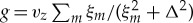 ,
,  and ξm=(kz+2πm/d)2/2me−μ. This offers a fast way to scan for Weyl nodes in the parameter space as no numerical diagonalization is required.
Before we present any numerical results, it is worthwhile to develop a qualitative picture of the low-energy excitations in such S–M superlattices. Consider the normal state dispersion (turning off superconductivity by setting Δ to zero) in the absence of M. For k∥=0, the low-energy excitations are located at large momenta around kz∼±kF. In the presence of a weak periodic potential  , the spectrum of the superlattice structure can be obtained by folding the free dispersion into the first Brillouin zone (BZ) kz∈[−π/d,π/d], which gives a set of Bloch bands, (kz+G)2/2me, all being restricted to small momenta since π/d≪kF. The spectrum acquires a gap as Δ is turned on and a sufficiently large Zeeman field will give rise to a set of zero-energy ABS formed below the superconducting gap Δ (see the blue lines corresponding to vso=0 in figure 3). Turning on the spin–orbit coupling will gap out zero-energy ABS with k∥≠0 and endow a topologically non-trivial spin structure with linear dispersion to the remaining zero-energy state located at k∥=0 (see the red line corresponding to vso≠0 in figure 3). The S–M proximity structure considered here differs from the well studied system of semiconductor nanowires [8] in its dimensionality. In three dimensions, linear dispersion in the vicinity of the nodes is known to be described by the Weyl Hamiltonian [4,20].
Figure 3.

The dispersion of energy with respect to kx at the Weyl nodes for different values of spin–orbit coupling vso for fixed vz=0.9Δ and d=9.5π. (Online version in colour.)
3. Weyl nodes
Two representative examples of the low-energy spectrum of the S–M superlattice are shown in figure 2. We will explicitly show that they correspond to one pair and two pairs of Weyl nodes, respectively. In both cases, we observe a linear energy-momentum dispersion near isolated points {k0} located on the kz-axis. At any of these diabolical points, the zero-energy state is doubly degenerate. Let us label these two degenerate states as  and
and  , or |±〉 for short. The low-energy physics near the node is described by an effective Hamiltonian which is a 2×2 matrix in the Hilbert space spanned by |±〉 with the general form [20]
 |
3.1 |
Here  are the pseudo-spin Pauli matrix in the ± space. The low-energy Bogoliubov quasi-particles thus resemble massless chiral fermions (Weyl fermions). The chirality refers to the locking of the pseudo-spin with respect to the momentum direction as described by h(q). The direction of h,
  , constitutes a mapping from a sphere in the momentum space enclosing the Weyl nodes to a unit sphere in pseudo-spin space. The topological invariant for this mapping is the winding number [4]
 |
3.2 |
where the integration is over a closed volume containing q=0, and ∂j=∂/∂qj. In the simplest example h=±q,  ; and for vij=λiδij,
  . Since
  resembles a spin-
 particle in a magnetic field, one can define the Berry connection and the corresponding flux density [20]. Then a Weyl node corresponds to a magnetic monopole with charge
  in the momentum space. For periodic systems, the net flux through the BZ and the net magnetic charge inside the BZ must be zero [20]. Therefore, Weyl nodes always appear in pairs of opposite charge
  . They are well separated in k space and topologically stable [20].
Figure 2.

Weyl nodes in S–M superlattices. Only the lowesteigen energy, E(kx,ky= 0,kz), is shown. The blue line is its dispersion along the kz-axis inside the first BZ kz∈[−π/d,π/d]. Left panel: a single pair of Weyl nodes. The range of kx is kx/kF∈[−0.05,0.05], d=10π/kF, vz=2.5Δ. Right panel: two pairs of Weyl nodes for kx/kF∈[−0.015,0.015], d=9.5π/kF, vz=Δ. Here d is the superlattice period, vz is the strength of the Zeeman field, and vso is the spin–orbit coupling. We choose Δ=0.05μ and vso=5Δ. (Online version in colour.)
It is important to conduct the search for zero-energy states in the entire momentum space. Figure 3 shows the energy-momentum dispersion along the kx-axis for fixed  for various values of vso and the fixed Zeeman term, vz=0.9Δ. For very small spin–orbit coupling, the slope around kx=0 is vanishingly small, and there are many other low-lying states at larger values of kx that are sufficiently close to zero energy. These are ABS ubiquitously found in superconducting proximity structures. For example, for vso=0, the structure reduces to a superconductor–ferromagnet (S–F) superlattice. Then, from semiclassical considerations, it is expected that a series of ABS with finite kx will be formed between two adjacent F layers. The slope near kx=0 increases with vso. At the same time, other ABS at finite kx are increasingly gapped out. For sufficiently large vso, the Weyl nodes on the kz-axis are the only zero-energy states. In other words, spin–orbit coupling is crucial for the S–M superlattice to qualify as a Weyl superconductor. Strong spin–orbit coupling is preferred because it gives a steep dispersion around the node, making it well separated from other subgap excitations (see the discussion in the last paragraph of §2).
We have numerically computed the pseudo-spin texture near the Weyl nodes. Considering a state  with positive energy and a momentum k on one of the cones shown in figure 2, and constructing a two-component spinor |χ〉 by projecting
  onto the |±〉 basis formed by the zero-energy states at the given node, then:
 |
3.3 |
The three components of the h vector are the expectation values of the corresponding Pauli matrices  in state |χ〉,
| 3.4 |
| 3.5 |
| 3.6 |
The result is illustrated in figure 4 for the case of a single pair of Weyl nodes. The pseudo-spin texture suggests that
| 3.7 |
for the two nodes at  , respectively. Using the formula for
  above, we can rescale q to find their corresponding topological charge,
  (i.e. the two Weyl nodes have opposite topological charge (chirality)). The characteristic spin texture around two pairs of Weyl nodes is illustrated in figure 5. We observe that the topological charges of the two nodes on the positive kz-axis, such as (c) and (d), are opposites of each other. The two nodes at the mirroring position,
  , such as (b) and (c), also possess opposite charges.
Figure 4.

The pseudo-spin h (arrows) on equal energy contours (grey lines) near a pair of Weyl nodes. Note that ky=0 and hx=0. To show the (three-dimensional) h vector on the (kx,kz) plane, we plot hz along the kz-axis and hy along the kx-axis. Panel (a) is near the node at  , whereas panel (b) is near the node at
  . Δ=0.05μ, vso=0.5μ, vz=0.05μ and d/π=10/kF. (Online version in colour.)
Figure 5.

(a–d) The pseudo-spin h on equal energy contours near two pairs of Weyl nodes. ky=0 and hx=0, hz is along the kz-axis and hy is along the kx-axis. Δ=0.05μ, vso=0.5μ, vz=0.05μ and d/π=9.5/kF. (Online version in colour.)
4. Fermi arcs
The ABS formed at the surface of a Weyl superconductor are very peculiar. The zero-energy surface states in the two-dimensional momentum space (such as the surface BZ) take the shape of a continuum line connecting two Weyl nodes of opposite topological charges. Its topological origin has been discussed in the context of Weyl semimetals [15,20] and the A phase of 3He [23,24], and so will not be repeated here. Instead, we explicitly compute the spectrum of S–M superlattice structures that have a finite width L in the y-direction to demonstrate the Fermi lines. Since the wave function has to vanish at y=0 and y=L, we can expand it in the sine Fourier series,
| 4.1 |
Then the BdG equation becomes
| 4.2 |
where we have defined
 |
4.3 |
with  , kn=nπ/L, and
  with
with
| 4.4 |
In the numerical solution of the BdG equation, equation (4.2), it is important to keep enough kn.
Figure 6 shows the calculated finite-slab spectrum for a single pair (figure 6a) and two pairs (figure 6b) of Weyl nodes. In the former case, a continuous line of zero-energy states is formed along the kz-axis connecting the bulk Weyl node at  to that at
  . These Fermi arc (in this case just a straight line) states are absent in the bulk spectrum and correspond to the surface states at y=0 and L. In fact, a very small gap is visible due to the hybridization of the two surfaces that are of finite distance L apart. In the latter case, the Fermi arc connects the two bulk Weyl nodes on the positive kz-axis. (There is another arc along the negative kz-axis, which is not shown.) This is in accordance with the topological charge of the nodes found above from the spin texture.
Figure 6.

Fermi arcs on the surface of the S–M superlattice. The plot shows the low-energy spectrum ϵ(kx=0,kz) of a finite-slab y∈[0,L]. (a) The arc connects k0 and −k0 (only the positive kz is shown). kFd=50, vz=0.6Δ. (b) The Fermi arc along the kz-axis connects two Weyl nodes on the positive kz-axis. kFd=30, vz=1.1Δ. In both cases, kFL=200, μ=20Δ, vso=Δ. (Online version in colour.)
5. Phase diagram
The spin texture and the Fermi arc surface states presented above unambiguously established the existence of pairs of Weyl nodes in S–M periodic structures. We have systematically scanned the parameter space of this model and the resultant phase diagram is shown in figure 7. Most strikingly, one observes a series of lobes (light grey regions,  ) that feature single pairs of Weyl nodes, similar to those shown in the left panel of figure 2. Approximately, each lobe appears when kFd=nπ (
 ) and vz>Δ. The dark black regions (
 ) represent phases with two pairs of Weyl nodes. They also appear as a regular array but are well separated from each other and much smaller in area compared to
  . In fact,
  can be viewed as the overlapping regions of two adjacent
  phases, as seen in the inset of figure 7, which shows the details near d/π=10. In the rest of the phase diagram (white regions,
  ), the spectrum is gapped, even though the gap may be numerically small (see, for example, the spectrum at point A shown in the first subpanel).
Figure 7.

The phase diagram of the nodal structure of the S–M superlattice as a function of superlattice spacing d and Zeeman field vso in the regime of sufficiently strong spin–orbit coupling is shown in (a). The shaded (light grey) region corresponds to one pair of Weyl nodes, and the dark black region corresponds to two pairs of Weyl nodes. The spectrum is gapped in the white region. Δ=0.05μ; the superlattice period d is measured in 1/kF. The inset shows a zoom of the region around dkF/π=10. By selecting a set of points at (blue) ×’s labelled by (blue) letters A–F, thechange of low-energy spectrum along a vertical cut is shown in (b). An arrow ( ) is used to distinguish labels for different points. (Online version in colour.)
The evolution of the spectrum along a vertical cut in the phase diagram, from point A to point F, is illustrated in the subpanels of figure 7. As vz is increased at this particular value of d, the lowest branch of the spectrum is pushed down by the increasing Zeeman splitting to touch E=0, entering the  phase (A
 B). With further increase of vz, the newly born pair of Weyl nodes with opposite charges become increasingly detached from each other, with one heading towards kz=0 and the other towards the BZ boundary. The latter gets gapped out once it reaches the BZ boundary where it annihilates with its mirror image living on the negative kz-axis, thus marking the transition from the
  phase to the
  phase (C
 D). Further increase of vz will push the spectrum away from E=0, and the two Weyl nodes of opposite charge annihilate each other at kz=0, leaving behind a vacuum (E
 F).
F).
The Kronig–Penney model for the SM supelattice is idealistic and neglects a few effects that may be important when the M layer becomes thick and/or then its exchange field becomes very strong. The order parameter will be suppressed by the M, and its spatial profiles of Δ(z) have to be determined self-consistently. We expect the Weyl nodes will persist as long as the suppression is not severe. In extreme cases, the order parameters at the opposite sides of the M layer may prefer to develop a phase difference of π, analogous to the π junction. The resulting SM superlattice will be analogous to a pair density wave or Larkin–Ovchinnikov superconductor, and its spectrum has to be found separately.
6. Lattice model
Now we turn to S–M heterostructures described by tight-binding Hamiltonians defined on discrete lattices. We will illustrate this approach by focusing on the superconductor–magnetic topological insulator (S–TI) superlattice structure proposed in [18]. However, in contrast to Meng & Balents [18], we start from microscopic models of S and TI instead of the low-energy surface degrees of freedom (i.e. the Dirac electrons). Compared to the continuum model above, the lattice model can sometimes offer more realistic descriptions of the material-specific properties, especially regarding the coupling between S and M, and at the limit where the thickness of S and M are comparable to each other. As a result, the lattice model can potentially provide more quantitative predictions of the design parameters of Weyl superconductors.
For simplicity, we model both S and TI on cubic lattice with lattice constant a. Each unit cell of the superlattice consists of NS layers of S and NT layers of TI stacked along the z-direction. If i is the layer index, the eigenvalue problem has a tri-diagonal structure
| 6.1 |
Here Ti,i+1 is the hopping matrix coupling layer i to the neighbouring layer i+1, Hi is the Hamiltonian for the ith layer, and Ψi is the wave function at the ith layer. Note that the transverse momentum k∥=(kx,ky) is conserved. For each S layer, i.e. i∈[1,NS],
 |
6.2 |
where  and k is measured in units of 1/a. The hopping between two adjacent S layers is simply
 |
6.3 |
For example, we take ts=0.18 eV and μ=−4ts. Considering Bi2Se3 as a prime example of three-dimensional Z2 topological insulators, and modelling each TI layer by [25]
| 6.4 |
where  . We choose the basis (|p+↑〉, |p+↓〉, |p−↑〉, |p−↓〉), where p± labels the hybridized pz orbital with even (odd) parity [26]. The Gamma matrices are defined as
  ,
,  , with
  (
( ) being the Pauli matrices in the orbital (spin) space. vz is the Zeeman splitting for magnetically doped Bi2Se3 [27–29]. The coupling between two adjacent TI layers is given by
| 6.5 |
The isotropic version of  and
and  , with a1=a2, b1=b2, was proposed by Qi et al. as a minimal model for three-dimensional topological insulators [30]. To mimic Bi2Se3, we set the lattice spacing a=5.2 Å , which gives the correct unit cell volume, and ai=Ai/a, bi=Bi/a2 for i=1,2. The numerical values of M, Ai, Bi are given in [26]. With these parameters, our model yields the correct band gap and surface dispersion, and it also reduces to the continuum k⋅p Hamiltonian (the Bernevig–Hughes–Zhang model) in the small k limit [26], aside from a topologically trivial ϵ0(k) term. To describe the superconducting proximity effect, we have to generalize the TI Hamiltonian above into the particle-hole space. For i∈[NS+1,NS+NT],
 |
6.6 |
and accordingly,
 |
6.7 |
Finally, the hopping from S to TI is a 4×8 matrix,
 |
6.8 |
with
 |
6.9 |
Here J± is the overlap integral between the p-orbital p± of TI and the s-like orbital of S. For simplicity, we assume the spin is conserved during the hopping, and from the orbital symmetry, J+=−J−=J, where J can be tuned from weak to strong [25]. Small J mimics a large tunnelling barrier between S and TI, while large J describes good contact, i.e. strong coupling between S and TI.
A standard lattice Fourier transform from the layer index i to quasi-momentum kz inside the reduced BZ, [−π/Na,π/Na] with N=NS+NT, gives each Ti,i+1 a phase factor eikza. The Hamiltonian of one unit cell of the superlattice is a matrix of the size 4NS+8NT, subject to periodic boundary conditions. Then a numerical diagonalization yields the band structure E(kx,ky,kz) of the S–TI superlattice.
7. Andreev-bound states at the S–TI interface
Before discussing the S–TI multilayer system, it is worthwhile to first consider the spectral properties of a single S–TI interface, which have been studied extensively since the pioneer work of Fu & Kane [3]. Comparison with these known results will serve as a critical check of our lattice model presented above. It also establishes the connection between the microscopic model here and the effective model of Fu and Kane for the S–TI interface [3], as well as that of Meng and Balents for the S–TI superlattice [18].
The spectrum of a single S–TI interface can be conveniently extracted from our lattice model by taking various limits. Firstly, by setting J=0 and vz=0 (but keeping finite Δ), the low-energy spectrum reduces to the surface states of the topological insulator. As the thickness NT is reduced, the linear Dirac spectrum acquires a gap due to the hybridization between two TI surfaces [31]. For example, the gap is around 0.012eV when NT=8.
Secondly, by setting vz=0 and keeping NT and NS large, the low-energy spectrum E(kx,ky,kz=0) reduces to that of a single S–TI interface, since all the interfaces are sufficiently far apart and essentially decoupled from each other. Note that at this limit, the BZ is very small, and the dispersion along kz is negligible, so we set kz=0. Figure 8 shows the evolution of the subgap spectrum as J is increased from the tunnelling to the strong coupling limit. In each case, the dispersion of the subgap modes can be fit well by formula  which follows from Fu and Kane’s phenomenological model [3],
 |
7.1 |
where hs describes the helical Dirac electrons [3,26],
| 7.2 |
This suggests that the Fu–Kane model is valid for a broad range of coupling strengths between S and TI. Yet, as clearly seen in figure 8, the effective parameters (μs,Δs,vs) in HFK depend sensitively on J. They may get strongly renormalized from their respective nominal values estimated from the bulk parameters by the proximity effect (the coupling to S). For device applications, e.g. for the generation and manipulation of Majorana zero modes, a large Δs and thus a strong S–TI coupling is preferred. At this limit it is more natural to think of the interface state as the ABS which penetrates into the superconductor over the coherence length but decays rapidly (over a distance on the atomic scale) in the TI [21]. The lattice calculation presented here is in agreement with the wave function calculation in [21] and the Green function calculation in [32].
Figure 8.

Andreev-bound states at theS–TI interface. NS=NT=20, ky=kz=0. The blue, green and red curves are for J/ts=0.2, 0.5, 1, respectively. Here, vz=0, Δ= 14 meV, ts=0.18 eV and μ=−4ts. (Online version in colour.)
Thirdly, vz can be easily incorporated into the Fu–Kane Hamiltonian. For a single S–TI interface, it opens up a Zeeman gap at k∥=0. Using this as the starting point, Meng & Balents [18] analysed the effective Hamiltonian of the S–TI superlattice and arrived at a very clean phase diagram in the plane of vz and Δ.
8. Weyl fermions
In search of Weyl nodes within our microscopic lattice model, we shall focus on ‘ideal’ conditions, provided they seem experimentally feasible. High-temperature superconductor (BSCCO) in proximity to Bi2Se3 was reported to induce a gap of 15 meV, and the pairing symmetry was postulated to be s-wave because no d-wave nodes were observed [33,34]. In comparison, the gap of Bi2Se3 grown on NbSe3 is in the order of meV [35]. We will consider a fairly large gap, Δ=14 meV. The Zeeman field vz can exceed the value of Δ. For example, chromium-doped Bi2(SexTe1−x)3 has an exchange gap of 40 meV [29], and Bi2Se3 doped with Mn [27,36] develops an exchange gap ranging from 10 to 60 meV. As to the number of layers for each material, we will consider, for example, NS=5, NT=3, which gives a large BZ, allowing kz to have significant dispersion. Certain natural multilayer heterostructures (not superconducting) of TI such as (PbSe)5(Bi2Se3)3m have been reported [37]. Epitaxial growth of TI films with 1–12 quintuple layers on superconducting substrate has been successfully demonstrated [38]. Also, the superconductor BaBiO3 with Tc∼30 K was predicted to turn into a TI upon electron doping [39]. This implies that the S–TI superlattice may even be realized based on a single compound by modulated electric or chemical doping.
Figure 9 shows the low-energy part of E(kx=ky=0,kz) for vz=3Δ (blue) and 5Δ (orange). They have one pair and two pairs of Weyl nodes on the kz-axis, respectively. One can explicitly check that these nodes are the only zero-energy states within the reduced BZ, and the energy E is indeed linear in k−k0. Figure 10 summarizes the location (and number) of the Weyl nodes on the positive kz-axis as the Zeeman field vz is increased. The phases and phase boundary can be easily read from figure 10. Taking NS=5 (the empty circle) for example, for vz<1.6Δ the spectrum is gaped and the system is in phase  . For vz∈[1.6Δ,4Δ] there is only one node on the positive kz-axis. And the node moves away from kz=0 as vz is increased. This is phase
  . For vz>4Δ, a second nodal point appears at the BZ boundary kz=π/(Na). The system enters the
  phase. Overall, the evolution of the nodal structure here is similar to that of the continuum model discussed above. Figure 10 also compares the phases for increasing numbers of superconducting layers. As a general trend, the critical vz required for the
  to appear increases with NS. At the limit of large NS, the dispersion along kz becomes very flat.
Figure 9.

One pair versus two pairsof Weyl nodes in the S–TI superlattice. The blue (orange) spectrum corresponds to vz=3Δ (5Δ). NS=5, NT=3, with J=0.7ts, ts=0.18 eV and Δ=14 meV. (Online version in colour.)
Figure 10.

The number and location of Weyl nodes in the S–TI superlattice as functions of the Zeeman field vz for NS=5 (circles), NS=7 (diamonds), NS=9 (triangles) and NS=11 (squares). We fix NT=3 with J=0.7ts, ts=0.18 eV and Δ=14 meV. (Online version in colour.)
9. Concluding remarks
We have presented two complementary approaches to model and compute the properties of S–M superlattice structures. The first approach is based on a simple continuum model where M is described by periodic spin-active potentials that are spatially thin compared to the thickness of the superconductor, and accordingly, the size of the unit cell can be larger than the superconducting coherence length. The second approach is based on a tight-binding lattice model describing alternative layers of S and TI, both of which can be only several layers thick with a tunable coupling strength between the two materials. In both models, we find phases that have one or two pairs of Weyl nodes. Together with previous results based on tunnelling Hamiltonians [18], our study unambiguously establishes that (i) S–M periodic structures can behave as Weyl superconductors at low energies, and (ii) for this to occur, neither topological insulators nor Dirac electrons are necessary, only the right combination of spin–orbit coupling and Zeeman splitting is required. These observations generalize the proposals of realizing gapped topological superconductors featuring Majorana zero modes in one and two dimensions [6–10] to gapless topological superconductors in three dimensions using periodic structures of S and M. We hope that the theoretical analysis presented here can stimulate experimental work to explore these ideas.
The emergence of Weyl fermions at low energies out of the vacuum of a conventional s-wave superconductor is quite striking. While these low-energy quasi-particles can be viewed as the ABS formed at the S–M interface dispersing with kz and crossing zero energy at isolated k points, they are located in k space near k=0 (for kFd≫1) instead of being around the original Fermi surface |k|=kF. In other words, the spectral weight is transferred not only from high to low energy, but also from high to low momentum, by the presence of the periodic spin-active potential. In this paper, we have only considered one-dimensional S–M superlattice structures. It is very likely that equally interesting phenomena may rise for ‘metamaterials’ of superconductors and spin-active materials that have more complicated periodic structures in even higher dimensions.
Acknowledgements
We thank Matthias Eschrig, Mahmoud Lababidi and Sungkit Yip for stimulating discussions. We also acknowledge the Institute for Nuclear Theory at the University of Washington for its hospitality (INT-15-1 workshop) and the Department of Energy for partial support during the completion of this work.
Data accessibility
This article has no additional data.
Competing interests
We declare we have no competing interests.
Funding
This work is supported by AFOSR FA9550-16-1-0006 and NSF PHY-1205504.
References
- 1.Hasan MZ, Kane CL. 2010. Colloquium: topological insulators. Rev. Mod. Phys. 82, 3045–3067. ( 10.1103/RevModPhys.82.3045) [DOI] [Google Scholar]
- 2.Qi X-L, Zhang S-C. 2011. Topological insulators and superconductors. Rev. Mod. Phys. 83,1057–1110. ( 10.1103/RevModPhys.83.1057) [DOI] [Google Scholar]
- 3.Fu L, Kane CL. 2008. Superconducting proximity effect and majorana fermions at the surface of a topological insulator. Phys. Rev. Lett. 100, 096407 ( 10.1103/PhysRevLett.100.096407) [DOI] [PubMed] [Google Scholar]
- 4.Volovik G. 2009. The universe in a helium droplet. New York, NY: Oxford University Press. [Google Scholar]
- 5.Kallin C, Berlinsky J. 2015. Chiral Superconductors. (http://arxiv.org/abs/1512.01151).
- 6.Sau JD, Lutchyn RM, Tewari S, Das Sarma S. 2010. Generic new platform for topological quantum computation using semiconductor heterostructures. Phys. Rev. Lett. 104, 040502 ( 10.1103/PhysRevLett.104.040502) [DOI] [PubMed] [Google Scholar]
- 7.Lutchyn RM, Sau JD, Das Sarma S. 2010. Majorana fermions and a topological phase transition in semiconductor-superconductor heterostructures. Phys. Rev. Lett. 105, 077001 ( 10.1103/PhysRevLett.105.077001) [DOI] [PubMed] [Google Scholar]
- 8.Alicea J. 2010. Majorana fermions in a tunable semiconductor device. Phys. Rev. B 81, 125318 ( 10.1103/PhysRevB.81.125318) [DOI] [Google Scholar]
- 9.Oreg Y, Refael G, von Oppen F. 2010. Helical liquids and majorana bound states in quantum wires. Phys. Rev. Lett. 105, 177002 ( 10.1103/PhysRevLett.105.177002) [DOI] [PubMed] [Google Scholar]
- 10.Potter AC, Lee PA. 2011. Engineering ap+ipsuperconductor: comparison of topological insulator and Rashba spin-orbit-coupled materials. Phys. Rev. B 83, 184520 ( 10.1103/PhysRevB.83.184520) [DOI] [Google Scholar]
- 11.Mourik V, Zuo K, Frolov SM, Plissard SR, Bakkers EPAM, Kouwenhoven LP. 2012. Signatures of majorana fermions in hybrid superconductor-semiconductor nanowire devices. Science 336, 1003–1007. ( 10.1126/science.1222360) [DOI] [PubMed] [Google Scholar]
- 12.Nadj-Perge S, Drozdov IK, Li J, Chen H, Jeon S, Seo J, MacDonald AH, Bernevig BA, Yazdani A. 2014. Observation of majorana fermions in ferromagnetic atomic chains on a superconductor. Science 346, 602–607. ( 10.1126/science.1259327) [DOI] [PubMed] [Google Scholar]
- 13.Beenakker C. 2013. Search for majorana fermions in superconductors. Ann. Rev. Condens. Matt. Phys. 4, 113–136. ( 10.1146/annurev-conmatphys-030212-184337) [DOI] [Google Scholar]
- 14.Alicea J. 2012. New directions in the pursuit of Majorana fermions in solid state systems. Rep. Progress Phys. 75, 076501 ( 10.1088/0034-4885/75/7/076501) [DOI] [PubMed] [Google Scholar]
- 15.Wan X, Turner AM, Vishwanath A, Savrasov SY. 2011. Topological semimetal and Fermi-arc surface states in the electronic structure of pyrochlore iridates. Phys. Rev. B 83, 205101 ( 10.1103/PhysRevB.83.205101) [DOI] [Google Scholar]
- 16.Yang K-Y, Lu Y-M, Ran Y. 2011. Quantum Hall effects in a Weyl semimetal: possible application in pyrochlore iridates. Phys. Rev. B 84, 075129 ( 10.1103/PhysRevB.84.075129) [DOI] [Google Scholar]
- 17.Delplace P, Li J, Carpentier D. 2012. Topological Weyl semi-metal from a lattice model. Europhys. Lett. 97, 67004 ( 10.1209/0295-5075/97/67004) [DOI] [Google Scholar]
- 18.Meng T, Balents L. 2012. Weyl superconductors. Phys. Rev. B 86, 054504 ( 10.1103/PhysRevB.86.054504) [DOI] [Google Scholar]
- 19.Burkov AA, Balents L. 2011. Weyl semimetal in a topological insulator multilayer. Phys. Rev. Lett. 107, 127205 ( 10.1103/PhysRevLett.107.127205) [DOI] [PubMed] [Google Scholar]
- 20.Vafek O, Vishwanath A. 2014. Dirac fermions in solids: from high-tccuprates and graphene to topological insulators and weyl semimetals. Ann. Rev. Condens. Matter Phys. 5, 83–102. ( 10.1146/annurev-conmatphys-031113-133841) [DOI] [Google Scholar]
- 21.Lababidi M, Zhao E. 2011. Microscopic simulation of superconductor/topological insulator proximity structures. Phys. Rev. B 83, 184511 ( 10.1103/PhysRevB.83.184511) [DOI] [Google Scholar]
- 22.Michelsen J, Grein R. 2012. Superconducting proximity effect in semiconductor thin films with spin-splitting and spin-orbit interaction. (http://arxiv.org/abs/1208.1090) [cond-mat.supr-con].
- 23.Tsutsumi Y, Ichioka M, Machida K. 2011. Majorana surface states of superfluid 3He A and B phases in a slab. Phys. Rev. B 83, 094510 ( 10.1103/PhysRevB.83.094510) [DOI] [Google Scholar]
- 24.Silaev MA, Volovik GE. 2012. Topological Fermi arcs in superfluid3He. Phys. Rev. B 86, 214511 ( 10.1103/PhysRevB.86.214511) [DOI] [Google Scholar]
- 25.Zhao E, Zhang C, Lababidi M. 2010. Mott scattering at the interface between a metal and a topological insulator. Phys. Rev. B 82, 205331 ( 10.1103/PhysRevB.82.205331) [DOI] [Google Scholar]
- 26.Zhang H, Liu C-X, Qi X-L, Dai X, Fang Z, Zhang S-C. 2009. Topological insulators in Bi2Se3, Bi2Te3 and Sb2Te3 with a single Dirac cone on the surface. Nat. Phys. 5, 438–442. ( 10.1038/nphys1270) [DOI] [Google Scholar]
- 27.Chen YL. et al. 2010. Massive dirac fermion on the surface of a magnetically doped topological insulator. Science 329, 659–650. ( 10.1126/science.1189924) [DOI] [PubMed] [Google Scholar]
- 28.Chang C-Z. et al. 2013. Experimental observation of the quantum anomalous hall effect in a magnetic topological insulator. Science 340, 167–170. ( 10.1126/science.1234414) [DOI] [PubMed] [Google Scholar]
- 29.Zhang J. et al. 2013. Topology-driven magnetic quantum phase transition in topological insulators. Science 339, 1582–1586. ( 10.1126/science.1230905) [DOI] [PubMed] [Google Scholar]
- 30.Qi X-L, Hughes TL, Zhang S-C. 2008. Topological field theory of time-reversal invariant insulators. Phys. Rev. B 78, 195424 ( 10.1103/PhysRevB.78.195424) [DOI] [Google Scholar]
- 31.Zhang Y. et al. Crossover of the three-dimensional topological insulator Bi2Se3 to the two-dimensional limit. Nat. Phys. 6, 584–588. ( 10.1038/nphys1689) [DOI] [Google Scholar]
- 32.Grein R, Michelsen J, Eschrig M. 2012. A numerical study of the superconducting proximity effect in topological surface states. J. Phys. Conference Series 391, 012149 ( 10.1088/1742-6596/391/1/012149) [DOI] [Google Scholar]
- 33.Wang E. et al. 2013. Fully gapped topological surface states in Bi2Se3 films induced by a d-wave high-temperature superconductor. Nat. Phys. 9, 621–625. ( 10.1038/nphys2744) [DOI] [Google Scholar]
- 34.Zareapour Pl. et al. 2012. Proximity-induced high-temperature superconductivity in the topological insulators Bi2Se3 and Bi2Te3. Nat. Commun. 3, 1056–1050. ( 10.1038/ncomms2042) [DOI] [PubMed] [Google Scholar]
- 35.Wang M-X. et al. 2012. The coexistence of superconductivity and topological order in the Bi2Se3 thin films. Science 336, 52–55. ( 10.1126/science.1216466) [DOI] [PubMed] [Google Scholar]
- 36.Xu S-Y. et al. 2012. Hedgehog spin texture and Berry’s phase tuning in a magnetic topological insulator. Nat. Phys. 8, 616–622. ( 10.1038/nphys2351) [DOI] [Google Scholar]
- 37.Nakayama K, Eto K, Tanaka Y, Sato T, Souma S, Takahashi T, Segawa K, Ando Y. 2012. Manipulation of topological states and the bulk band gap using natural heterostructures of a topological insulator. Phys. Rev. Lett. 109, 236804 ( 10.1103/PhysRevLett.109.236804) [DOI] [PubMed] [Google Scholar]
- 38.Xu J-P. et al. 2012. Artificial topological superconductor by the proximity effect. Phys. Rev. Lett. 112, 217001 ( 10.1103/PhysRevLett.112.217001) [DOI] [Google Scholar]
- 39.Yan B, Jansen M, Felser C. 2013. A large-energy-gap oxide topological insulator based on the superconductor BaBiO3. Nat. Phys. 9, 709–711. ( 10.1038/nphys276210.1038/nphys2762) [DOI] [Google Scholar]
Associated Data
This section collects any data citations, data availability statements, or supplementary materials included in this article.
Data Availability Statement
This article has no additional data.