Abstract
We report quantitative characterization of the high temperature oxidation process by using electron tomography and energy-dispersive X-ray spectroscopy. As a proof of principle, we performed 3D imaging of the oxidation layer of a model system (Mo3Si) at nanoscale resolution with elemental specificity and probed the oxidation kinetics as a function of the oxidation time and the elevated temperature. Our tomographic reconstructions provide detailed 3D structural information of the surface oxidation layer of the Mo3Si system, revealing the evolution of oxidation behavior of Mo3Si from early stage to mature stage. Based on the relative rate of oxidation of Mo3Si, the volatilization rate of MoO3 and reactive molecular dynamics simulations, we propose a model to explain the mechanism of the formation of the porous silica structure during the oxidation process of Mo3Si. We expect that this 3D quantitative characterization method can be applied to other material systems to probe their structure-property relationships in different environments.
Introduction
3D structural analysis is essential to understand the structure and property relationships of materials. One of the important 3D structural analysis techniques is electron tomography, which reconstructs 3D structural information from a tilt series of 2D electron microscopy images1–3. Although electron tomography has long been used in the biological sciences1, its application in the physical sciences has become more widespread over the last decade4–12. More recently, a groundbreaking technique, termed atomic electron tomography (AET)2, has been developed to determine the 3D structure of crystal defects and disordered materials such as grain boundaries, stacking faults, the core structure of edge and screw dislocations, point defects and chemical order/disorder at atomic resolution13–18. AET has also been applied to localize the 3D coordinates of individual atoms in materials and to correlate crystal defects with material properties at the single atomic level19,20. These successes of AET rely on powerful 3D reconstruction methods such as Equal Slope Tomography (EST) and GENeralized Fourier Iterative Reconstruction (GENFIRE)21–24. Compared to several popular tomographic methods, it has been demonstrated that EST and GENFIRE can achieve a higher resolution reconstruction from a limited number of projections with a missing wedge22,24. Here we apply EST to image the oxidation process of high temperature materials as a function of the oxidation time and the elevated temperature.
High temperature materials play an important role in a wide variety of technological areas, including energy, chemical and aerospace applications25–29. In particular there is a drive to find a material to surpass the high temperature limitations of directionally-solidified and single crystal Ni-based superalloys. The high temperature behavior of the Mo-Si-B material system has attracted interest due to its superior creep resistance and oxidation resistance at temperatures above 1200 °C27,30. It provides a promising class of potential candidates to replace currently widely used Ni-based superalloys. The oxidation protection of these alloys stems from the continuous outer layer of borosilica glass that develops upon high temperature oxidation exposure31. Usually the alloys consist of three phases: Mo in solid solution with Si and B (Moss), the intermetallic phases of Mo3Si (A15) and Mo5SiB (T2)27,32. The composition and phase consistency are important parameters in determining the oxidation response. It has been reported that a sufficient amount of T2 phase can improve the oxidation resistance by incorporating B into the silica scale as a fluxing agent, lowering the viscosity to enable flow and ultimately passivation31. However, boron additions also act to decrease the toughness and ductility of the alloys. The Moss phase is considered crucial for the mechanical properties but offers no intrinsic oxidation protection27,31. The oxidation of pure Moss causes a linear loss of mass due to continuous sublimation of volatile molybdenum oxides (typified by MoO3)27,33. To gain an optimal property balance between high temperature mechanical properties and oxidation resistance at high temperatures in Mo-Si-B alloys, it is necessary to design the material based on phase stability and control of microstructure.
In order to understand how the three phases interact with each other during the oxidation of Mo–Si–B alloys, it is necessary to know how they react with oxygen independently of each other. To date, significant efforts have been made in exploring the oxidation process of different phases of Mo-Si-B alloys. Rioult et al. performed a comparison between the oxidation of pure Mo, the A15 phase and the T2 phase33,34. They found that viscous SiO2 glass forms a porous, non-protective network of nano-channels after 10 minutes of oxidation at 1100 °C. It is generally believed that the porous network provides a pathway for oxygen diffusion to the substrate, causing continuous oxidation. However, the 3D structure of the oxidized A15 phase has not been studied yet. How the porous network connects and evolves with respect to the oxidation temperature and time remains elusive.
To establish a standard method for quantitative characterization of high temperature oxidation process in 3D, here we applied EST to reconstruct the 3D porous structure of the Mo3Si A15 phase formed at varying temperatures and oxidation times and performed a statistical analysis of the pore size. Using energy-dispersive X-ray spectroscopy (EDS), we also conducted an elemental analysis to obtain quantitative chemical information about the formation of MoO2. Reactive molecular dynamics (MD) simulations were further employed to understand the formation of the porous structure in Mo3Si. On the basis of our 3D reconstructions, we calculated the interfacial shape and normal distributions35,36 to quantify the morphology and directionality of our 3D porous structure, respectively. Our results provide new insights into the oxidation process of the Mo3Si structure and the formation of the porous SiO2 morphology during oxidation.
Results
3D reconstructions of oxidized porous Mo3Si structures at elevated temperatures
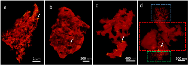
3D structures were reconstructed from four tilt series of scanning transmission electron microscopy (STEM) images of oxidized porous Mo3Si samples, annealed at different temperatures (Methods). Figure 1 shows volume-renderings of the four porous structures at different temperatures after 5 minutes of oxidation in air. The four samples are prepared using the same method but at different temperatures. The pore size is typically around 100–200 nm for all the structures. However, at 1100 °C there are many pores with a diameter as small as ~10 nm and a length as large as ~30 nm, which is about one order of magnitude smaller than the usual pore size. These small pores are also observed in the reconstructions of two other oxidized Mo3Si samples at 1100 °C (Supplementary Fig. 1a,b). To gain insight into the mechanism of pore formation, the oxidation of Mo3Si was simulated in all-atomic resolution using the reactive MD simulation37 (Supplementary Information). The simulations neglect the complex evaporation of MoOx phases for simplicity, and the resulting pores in thermodynamic equilibrium are much smaller than the experimentally measured ones. Also for MD simulations of the oxidation of large Mo3Si slabs with size of 20, 40, 100 nm, the SiO2 porous structure remains narrow and irregular with the pore diameter between 1 and 2 nm (Supplementary Fig. 2). These results suggest that the formation the mesoporous and macroporous structures in Fig. 1 is mainly due to the evaporation of the gaseous MoO3 instead of the oxidation. This process leads to large porous structures far from equilibrium. It has been reported that pure Mo forms MoO3 and evaporates rapidly above ~500 °C38 leaving only small voids. Our results indicate the high temperature yields small pores (~10 nm) due to volatilizing and the high diffusion rate of MoO3 vapor at high temperatures.
Figure 1.
3D volume-renderings of the reconstructed oxidized Mo3Si (A15) structures at different oxidation temperatures: 800 °C (a), 900 °C (b), 1000 °C (c) and 1100 °C (d). The blue and green squares indicate two highly porous regions with a small pore size (~10 to 30 nm). The red square indicates a region with a large pore size (~100–200 nm). The white arrows show the high intensity regions in the 3D reconstructions.
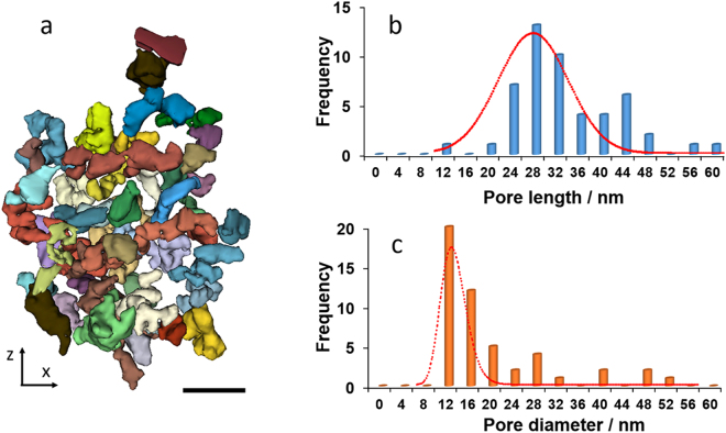
The porous structures are highly interconnected (almost ~ 100%) and irregular in shape. The segmentation of these smaller pores was done for the regions with the blue and green squares in Fig. 1d, and the size of the interconnecting points is smaller than 4 nm. The segmentation of the pores was obtained starting from the binarized stack of the initial reconstruction. First the exterior edges of the grain were defined and then a filled mask was applied. The pores were obtained by subtracting the initial binarized stack from the filled image of the grain. As shown in Fig. 2a, each colored isosurface represents a small pore that is separated from other pores by interconnecting points. A statistical analysis of the pore size is shown in Fig. 2b,c. The irregularly shaped pores have an average diameter of 10 nm and a length of 30 nm. Also, we calculated the porosity of these porous structures as 51% and 36% for the blue square region and green square region in Fig. 1d, respectively. We noticed that that the pore size and pore length can vary for different samples. Supplementary Fig. 1c,d show the average pore size and pore length to be 40 and 50 nm, respectively, for two other Mo3Si samples oxidized at 1100 °C for 5 min.
Figure 2.
Quantitative analysis of the 3D porous structure. (a) Individual pores selected from a highly porous region (the blue square in Fig. 1d). Statistical analysis of the pore length (b) and the pore diameter (c) distributions for the two highly porous regions (the blue and green squares in Fig. 1d). Scale bar, 100 nm.
Elemental analysis of porous silica structures with MoO2 islands
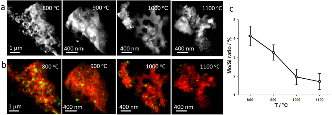
Figure 1 shows 3D reconstructions with very high intensity regions (white arrows), suggesting the segregation of Mo and Si. To test this hypothesis, we collected elemental information from these small high intensity islands within the 3D volume using STEM-EDS. For elemental analysis, high-angle annular dark-field (HAADF) STEM images and STEM-EDS mapping were simultaneously taken at the 0° projection of the same samples used for the electron tomography experiment. Figure 3a,b show the morphology of 3D porous structures and corresponding elemental mappings of Si Kα edge (red) and Mo Kα edge (green), respectively, at different oxidation temperatures. The correlation between the Mo signal in Fig. 3b and the high intensity structures in Fig. 3a indicates that Mo islands were formed in the porous silica structures. We also found that the high exposure temperature yielded a low proportion of the Mo signal.
Figure 3.
Morphology and composition analysis of porous structures of oxidized Mo3Si at different oxidation temperatures. (a) HAADF-STEM images at different oxidation temperatures. (b) Distribution of Si Kα (red) and Mo Kα (green) in the EDS composition maps of the sample structures in (a). (c) Quantification of the Mo/Si ratio as a function of the temperature. The error bars were calculated by quantifying several samples at each temperature.
To determine the Mo to Si ratio as a function of the temperature, we performed a quantitative analysis of the EDS spectra using samples prepared at different temperatures (Supplementary Information, Supplementary Fig. 3 and Supplementary Table 1). Figure 3c shows that the Mo/Si ratio decreases with the increase of the temperatures. From 800 °C to 1100 °C, the Mo/Si ratio decreases by a factor of 2, indicating fewer Mo-rich islands at higher temperatures. HAADF-STEM images show a clear MoO2 crystal structure, shown in Supplementary Fig. 4a,b and d. From these images, we calculated the crystal lattice constant to be ~5.5 Å for a and c, which is close to the published value for MoO2 (Supplementary Fig. 4c)39. Quantification of the EDS spectra from these regions further confirms that these are MoO2 but not Mo islands (Supplementary Fig. 5b,c). This observation is consistent with the reported phase equilibria over this temperature range, indicating that MoO2 and SiO2 are in equilibrium40.
3D reconstructions of oxidized porous Mo3Si with different oxidation times
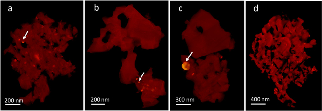
Besides the temperature, the effect of the oxidation time on the porous structures has also been studied. Four samples with different oxidation times were prepared and their 3D structures were reconstructed with EST. Figure 4 shows 3D volume renderings of the porous structures with the oxidation time of 5 min, 10 min, 30 min and 10 hours at 1100 °C in air. After oxidation for 5 min, 10 min and 30 min, MoO2 islands can be observed in porous silica (Fig. 4a–c). After 10 hours of oxidation, the whole volume is homogeneous and there is barely any MoO2 remaining in the porous regions (Fig. 4d). Although it is difficult to conclude the exact time when all of the MoO2 islands disappear, our data indicate that longer oxidation times lead to more complete oxidation and evaporation of Mo3Si.
Figure 4.
3D reconstructions of oxidized Mo3Si with different oxidation times: 5 minutes (a), 10 minutes (b), 30 minutes (c) and 10 hours (d). The white arrows indicate the high intensity regions, corresponding to the MoO2 islands.
Morphological Analysis of porous Mo3Si structure
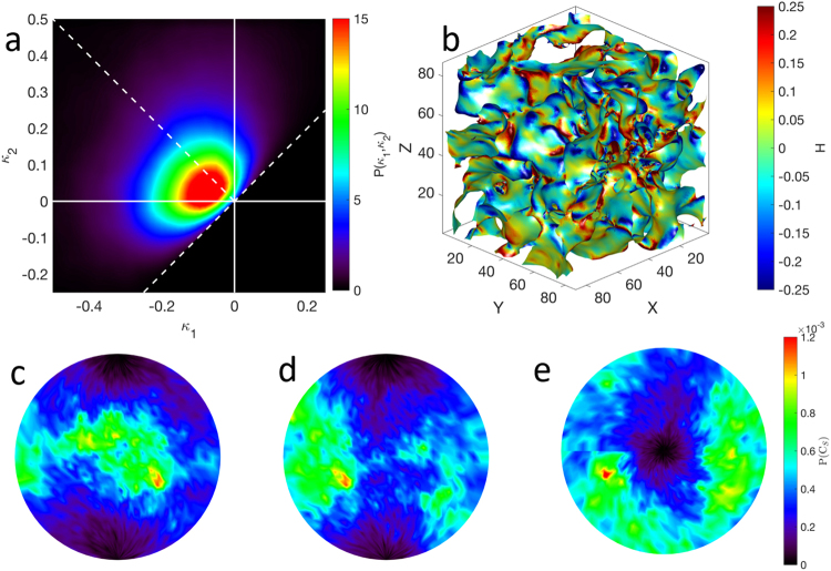
We quantified the morphology of a porous region (blue and green regions in Fig. 1d) using the interfacial shape distribution (ISD) method36. The ISD gives the probability P of locating an interfacial patch for a range of principal curvatures, ϰ1 and ϰ2, where ϰ2 > ϰ1 by definition. The principal curvatures are in turn related to the mean curvature H as H = ½(ϰ1 + ϰ2). In this classification, interfacial patches have a planar-like shape when ϰ1 = ϰ2 = 0; a cylindrical-like shape when ϰ1 = 0, ϰ2 > 0 or ϰ1 < 0, ϰ2 = 0; and a saddle-like shape when ϰ1 < 0 and ϰ2 < 0. Figure 5a,b show the ISD and corresponding illuminated mean curvatures of our porous structure oxidized at 1100 °C for 5 min.
Figure 5.
Interfacial shape distribution (a) and illuminated mean curvatures (b) of porous Mo3Si oxidized at 1100 °C. Interfacial normal distributions for porous Mo3Si oxidized at 1100 °C for projections along the +x (c), +y (d), and +z axes (e). The area under each IND is normalized to unity. The INDs indicate that the Mo3Si structure is isotropic.
We found that the interfacial morphology of porous Mo3Si is different from that in another bicontinous structure: nanoporous Au41. This suggests a fundamentally different mechanism underlying the formation of the porous Mo3Si structure. Nanoporous gold is created by dealloying Au-Ag solid solutions, resulting in open porosity, bicontinuous structures; it yields an ISD that is symmetric about the line ϰ2 = −ϰ1, corresponding to zero average mean curvature. By contrast, the ISD in Fig. 5a is not symmetric about the line ϰ2 = −ϰ1. Instead, the ISD indicates a much higher probability of cylindrical-like morphology, along line ϰ2 = 0 (H < 0). In Fig. 5b, the preponderance of light and dark blue colors decorating the structure supports this notion that the majority of the interface has a negative mean curvature.
In addition, the directionality of the porous Mo3Si structure was obtained by calculating its interfacial normal distribution (IND). The IND gives the probability P of finding an interfacial normal pointing in a given direction. Figure 5c–e. We show the IND using stereographic projections along the +x, +y, and +z axes. The INDs exhibit no peaks or prominent directions. Any variation in INDs is due to noise alone (see color bar). This means the structure is isotropic, as expected for a glass.
Discussion and Conclusions
The Mo-Si-B alloys have been reported as self-resistant materials from oxidation due to the formation of continuous borosilica glass layer developed upon high temperature exposure. However, there is value in understanding the mechanism of the oxidation process of the single Mo3Si A15 phase, as comprehension of the mechanisms at work informs deliberate design.
In evaluating the mechanism, it is instructive to consider the relative importance of the oxidation rate of Mo3Si and the volatilization rate of MoO3. Specific data for the oxidation rate of Mo3Si for the temperature range examined are not available, but a conservative estimation can be made by considering the oxidation behavior of Mo for which data are available. For the oxidation of Mo over the temperature range from 550 to 1700 °C the mass loss rate per unit area, (dMox/dt), is given by
| 1 |
where A = 0.504 g/cm2s, E = 82.4 kJ/mole, R is the gas constant and T is the temperature42. For the oxidation product of MoO3, the vapor pressure, P for solid MoO3 is represented by
| 2 |
Where P is in atm, the enthalpy of sublimation ΔHs = 136056 J/mole, and B = 13.62. Above the melting point of MoO3 at 795 °C, the vapor pressure is given by Eq. (2) with ΔH = 63,984 J/mole and B = 5.3842. The rate of mass loss per unit area, (dMevap/dt) by MoO3 evaporation can be evaluated by the Langmuir equation,
| 3 |
where m is the molecular weight. For MoO3 the dominant vapor species is reported as (MoO3)#43. The comparison of the relative reaction rates is presented in Fig. 6, indicating that the volatilization rate is much greater than the oxidation rate over the entire temperature range. Thus, as soon as MoO3 forms it evaporates to expose the substrate to further oxidation and to contribute additional SiO2 to the evolving porous silica.
Figure 6.
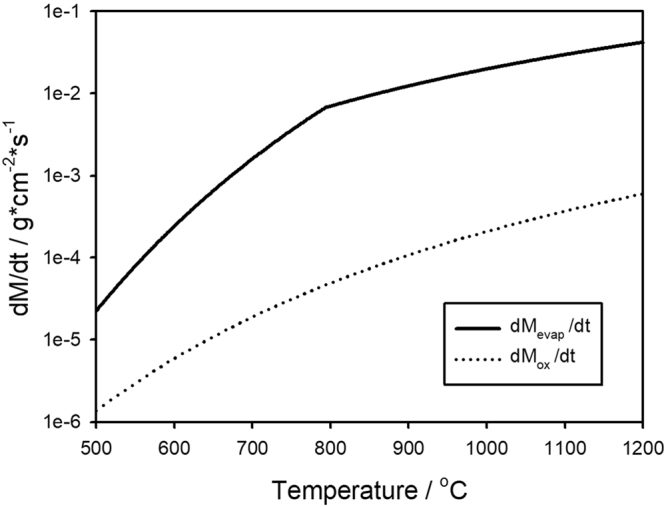
Quantitative comparison between the mass loss from the oxidation of Mo (dashed line) and the evaporation of MoO3 (solid line) as a function of the temperature.
From the consideration of the relative reaction rates, Fig. 7 shows the whole oxidation process of Mo3Si in air. Initially when bulk Mo3Si is exposed to oxygen, oxidation begins with formation of small islands of SiO2 and evaporation of MoO3 (Fig. 7a). Our results have revealed that at an intermediate time during the oxidation there is a porous silica layer with an approximate pore size of 100–200 nm with embedded Mo-rich islands, all on the top of bulk Mo3Si (Fig. 7b). The Mo-rich islands are mainly MoO2. Previous studies have shown the formation of silica at high temperatures is very viscous and limits the diffusion of oxygen27,33,34. As this oxidation proceeds, some regions can eventually reach a sufficient silica thickness to locally lower the partial pressure of oxygen to enable MoO2 formation instead of MoO3, thus resulting in trapped MoO2 in incompletely oxidized specimens. These trapped particles are not protected permanently, however; after exposed to sufficiently high temperature oxidation conditions for a long enough time, we hypothesize that Mo3Si will completely oxidize, yielding a pure porous silica structure by depletion of Mo (Fig. 7c).
Figure 7.
A proposed mechanism for the development of the porous SiO2 morphology. (a) Exposure of a Mo3Si A15 phase to O2 at a high temperature results in the formation of SiO2 and MoOx and the evaporation of gaseous MoO3. (b) Porous silica structure starts to develop due to the formation of voids formed after the evaporation MoO3. Some MoO2 islands also form due to the low O2 concentration in silica. (c) The Mo3Si A15 phase is fully oxidized, accompanying with the depletion of Mo and the complete formation of porous silica.
Using electron tomography and EDS, we obtained the 3D porous structure of oxidized Mo3Si at different elevated temperatures and oxidation times. We found that the porous structure highly depends on the oxidation temperature as it changes both the oxidation rate of Mo3Si and the evaporation rate of gaseous MoO3. We observed that MoO2 islands are embedded in porous silica of the oxidation layer. The amount of MoO2 decreases as the increase of the temperature. The pore size of silica is typically around 100–200 nm, but much smaller pore size was also observed after 5 minutes of oxidation at 1100 °C. By quantitatively analyzing the porous structure of Mo3Si at 1100 °C using ISD methods, we found the pore structure is isotropic, as expected for a glass. The ability to characterize the 3D structure of the oxidation layers in Mo3Si A15 phase with elemental specificity is expected to expand our understanding on how the oxidation behavior of Mo3Si evolves from early stage to mature stage. It is also clear from our results that the path to improve the oxidation resistance is based upon controlling the viscosity of silica so that it forms a continuous layer rather than a porous structure on the Mo3Si phase. Finally, we also want to point out that this quantitative characterization method could be applied to study the oxidation process of other material systems.
Methods
Synthesis of Mo3Si sample and oxidization process
Mo3Si alloy was produced by repeated arc melting of the elemental components in a titanium gettered chamber under Argon. The Mo and Si originate from 99.99% pure elemental reagents. The ingot is melted and re-melted five times to ensure homogeneity, while the ingot mass was measured between each melt to monitor losses. Only ingots with less than 1% loss are accepted. Next the ingot was cut with electrical discharge machining (EDM) into thin slices. These slices are then set onto an alumina boat and loaded into a tube furnace at the exposure temperature (i.e. 800 °C, 900 °C, 1000 °C and 1100 °C) for a certain amount of time (5 min, 10 min, 30 min and 10 hours) in air. After the exposure time, the samples are removed from the furnace to air cool.
TEM sample preparation and data acquisition
The four Mo3Si samples oxidized at 800, 900, 1000 and 1100 °C (typically ~200 μm thickness layer on top of the bulk Mo3Si) for 5 min and four Mo3Si samples oxidized at 1100 °C for 5 min, 10 min, 30 min and 10 hours were placed in agate mortar and immersed in ethanol, then gently pounded by agate pestle into smaller pieces, separately. The resultant solution was transferred to a plastic tub for sonication of 2 minutes for further dispersion. The supernatant solution was dropped by pipette onto a carbon film on 200 mesh copper transmission electron microscopy (TEM) grids (Ted Pella, Redding, CA). The samples were air-dried for 1 day before data acquisition.
For all TEM experiments, a Titan 60–300 equipped with a HAADF detector (Gatan, Pleasanton, CA) and four windowless silicon drift EDS detectors (FEI super-X) were used with a solid angle of 0.7 srad. The microscope was operated in STEM mode at 200 kV with an electron beam current of ~500 pA for STEM-EDS maps and ~40 pA for HAADF-STEM imaging. A typical total dose for the complete tomography series was ~2600 e−/Å2 and a typical total dose for an EDS map was ~1000 e−/Å2. Spectrum images have been acquired with drift-correction over ~120 s assuming a time-dependent linear drift model. For EDS analysis, we used a table of Cliff-Lorimer factors calculated for the 200 kV accelerating voltage to convert the integrated peaks to atomic concentration. The background of each spectrum was subtracted and the Kα of Mo and Kα of Si were fitted by Gaussian models using the Bruker Esprit software. To quantify Mo/Si ratio of porous structures, a fixed stoichiometry for oxides of Mo and Si was specified throughout the whole calculation.
All tilt series of HAADF-STEM projection images were typically acquired between −70° and 70° with a linear tilt step of 1°. The tilt range was limited by the shadowing of the sample holder (Hummingbird, Lacey, WA). HAADF-STEM images were acquired with a convergence semi-angle of 10 mrad at a detector inner semi-angle of 63 mrad and outer semi-angle of 305 mrad. Image size was 1024*1024 pixels with a pixel size from 1.13 nm to 6.47 nm depending on the size of the porous structure. We carefully checked the integrity of the samples before and after taking tomographic tilt series using zero degree projections and before and after EDS mapping, and no sample damage was visible (see e.g. Supplementary Fig. 6).
Data processing and EST reconstruction
To systematically remove the background, the mean of the background outside of the region of interest (ROI) of each projection was estimated and subtracted for every pixel. A binary mask was then created for the ROI by using thresholding and convolution, whereas the convolution was to maintain the smooth edge of the ROI. The binary mask was applied to the projection and all pixels outside of the mask were set to zero. To balance the signal to noise ratio, the desired resolution and the iterative reconstruction process, 2 × 2 pixel binning was performed for the projection. After background subtraction and binning, all the projections were aligned using the center of mass method13,15.
The reconstruction of the aligned projections was conducted using the EST algorithm. During the EST reconstruction, each projection image was assigned to the closest corresponding Fourier plane in the pseudo-polar fast Fourier transform (PPFFT) construct. Most of the angular differences between each measured (constant angular increment) projection and its closest PPFFT plane are less than 0.1°. The small angular difference would have a negligible effect on the 3D reconstruction22. The details of the EST algorithm can be found elsewhere13,15,17,19,21–24. In particular, it has been shown that EST can increase the spatial resolution and image contrast and reduce the missing wedge effect relative to other tomographic reconstruction methods.
Electronic supplementary material
Acknowledgements
We acknowledge support from ONR MURI “Understanding Atomic Scale Structure in Four Dimensions to Design and Control Corrosion Resistant Alloys” on Grant Number N00014-14-1-0675. This work was also supported by STROBE: A National Science Foundation Science & Technology Center under Grant No. DMR 1548924, the Office of Basic Energy Sciences of the US DOE (DE-SC0010378), and the NSF DMREF program (DMR-1437263). J.M. thanks support through the University of Strasbourg Institute for Advanced Study (USIAS) Fellowship. The HAADF-STEM imaging and EDS spectra collecting were performed at the Molecular Foundry, LBNL, which is supported by the Office of Science, Office of Basic Energy Sciences of the U.S. DOE under Contract No. DE-AC02-05CH11231.
Author Contributions
J.M. directed the research; M.T. and J.H.P. prepared the samples; J.Z., K.B. and P.E. conducted the experiments; J.Z., G.A.M., A.J.S., P.W.V., J.H.P., P.E. and J.M. performed the data analysis; C.C.D. and H.H. conducted the MD simulations; J.Z., M.T., G.A.M., A.J.S., C.C.D., H.H., P.W.V., J.H.P. and J.M. wrote the manuscript with contributions from all authors.
Competing Interests
The authors declare no competing interests.
Footnotes
Electronic supplementary material
Supplementary information accompanies this paper at 10.1038/s41598-018-28348-3.
Publisher's note: Springer Nature remains neutral with regard to jurisdictional claims in published maps and institutional affiliations.
References
- 1.Frank, J. Three-Dimensional Electron Microscopy of Macromolecular Assemblies (Oxford Univ. Press, 2006).
- 2.Miao J, Ercius P, Billinge SJL. Atomic electron tomography: 3D structures without crystals. Science. 2016;353:aaf2157. doi: 10.1126/science.aaf2157. [DOI] [PubMed] [Google Scholar]
- 3.Midgley PA, Dunin-Borkowski RE. Electron tomography and holography in materials science. Nat. Mater. 2009;8:271–280. doi: 10.1038/nmat2406. [DOI] [PubMed] [Google Scholar]
- 4.Spontak RJ, Williams MC, Agard DA. Three-dimensional study of cylindrical morphology in a styrene-butadiene-styrene block copolymer. Polymer. 1988;29:387–395. doi: 10.1016/0032-3861(88)90354-0. [DOI] [Google Scholar]
- 5.Koster AJ, Ziese U, Verkleij AJ, Janssen AH, De Jong KP. Three-dimensional transmission electron microscopy: a novel imaging and characterization technique with nanometer scale resolution for materials science. J. Phys. Chem. B. 2000;104:9368–9370. doi: 10.1021/jp0015628. [DOI] [Google Scholar]
- 6.Midgley PA, Weyland M. 3D electron microscopy in the physical sciences: the development of Z-contrast and EFTEM tomography. Ultramicroscopy. 2003;96:413–431. doi: 10.1016/S0304-3991(03)00105-0. [DOI] [PubMed] [Google Scholar]
- 7.Arslan I, Yates TJV, Browning ND, Midgley PA. Embedded nanostructures revealed in three dimensions. Science. 2005;309:2195–2198. doi: 10.1126/science.1116745. [DOI] [PubMed] [Google Scholar]
- 8.Kawase N, Kato M, Nishioka H, Jinnai H. Transmission electron microtomography without the “missing wedge” for quantitative structural analysis. Ultramicroscopy. 2007;107:8–15. doi: 10.1016/j.ultramic.2006.04.007. [DOI] [PubMed] [Google Scholar]
- 9.Xin HL, Ercius P, Hughes KJ, Engstrom JR, Muller DA. Three-dimensional imaging of pore structures inside low-κ dielectrics. Appl. Phys. Lett. 2010;96:223108. doi: 10.1063/1.3442496. [DOI] [Google Scholar]
- 10.Venkatakrishnan SV, et al. A model based iterative reconstruction algorithm for high angle annular dark field-scanning transmission electron microscope (HAADF-STEM) tomography. IEEE Trans. Image Process. 2013;22:4532–4544. doi: 10.1109/TIP.2013.2277784. [DOI] [PubMed] [Google Scholar]
- 11.Ersen O, Florea I, Hirlimann C, Pham-Huu C. Exploring nanomaterials with 3D electron microscopy. Mater. Today. 2015;18:395–408. doi: 10.1016/j.mattod.2015.04.004. [DOI] [Google Scholar]
- 12.Levin BDA, et al. Nanomaterial datasets to advance tomography in scanning transmission electron microscopy. Sci. Data. 2016;3:160041. doi: 10.1038/sdata.2016.41. [DOI] [PMC free article] [PubMed] [Google Scholar]
- 13.Scott MC, et al. Electron tomography at 2.4-angstrom resolution. Nature. 2012;483:444–447. doi: 10.1038/nature10934. [DOI] [PubMed] [Google Scholar]
- 14.Goris B, et al. Atomic-scale determination of surface facets in gold nanorods. Nat. Mater. 2012;11:930–935. doi: 10.1038/nmat3462. [DOI] [PubMed] [Google Scholar]
- 15.Chen C-C, et al. Three-dimensional imaging of dislocations in a nanoparticle at atomic resolution. Nature. 2013;496:74–77. doi: 10.1038/nature12009. [DOI] [PubMed] [Google Scholar]
- 16.Goris B, et al. Three-Dimensional Elemental Mapping at the Atomic Scale in Bimetallic Nanocrystals. Nano Lett. 2013;13:4236–4241. doi: 10.1021/nl401945b. [DOI] [PubMed] [Google Scholar]
- 17.Zhu C, et al. Towards three-dimensional structural determination of amorphous materials at atomic resolution. Phys. Rev. B. 2013;88:100201(R). doi: 10.1103/PhysRevB.88.100201. [DOI] [Google Scholar]
- 18.Haberfehlner G, et al. Formation of bimetallic clusters in superfluid helium nanodroplets analysed by atomic resolution electron tomography. Nat. Commun. 2015;6:8779. doi: 10.1038/ncomms9779. [DOI] [PMC free article] [PubMed] [Google Scholar]
- 19.Xu R, et al. Three-dimensional coordinates of individual atoms in materials revealed by electron tomography. Nat. Mater. 2015;14:1099–1103. doi: 10.1038/nmat4426. [DOI] [PubMed] [Google Scholar]
- 20.Yang Y, et al. Deciphering chemical order/disorder and material properties at the single-atom level. Nature. 2017;542:75–79. doi: 10.1038/nature21042. [DOI] [PubMed] [Google Scholar]
- 21.Miao J, Förster F, Levi O. Equally sloped tomography with oversampling reconstruction. Phys. Rev. B. 2005;72:052103. doi: 10.1103/PhysRevB.72.052103. [DOI] [Google Scholar]
- 22.Lee E, et al. Radiation dose reduction and image enhancement in biological imaging through equally-sloped tomography. J. Struct. Biol. 2008;164:221–227. doi: 10.1016/j.jsb.2008.07.011. [DOI] [PMC free article] [PubMed] [Google Scholar]
- 23.Mao Y, Fahimian BP, Osher SJ, Miao J. Development and optimization of regularized tomographic reconstruction algorithms utilizing equally-sloped tomography. IEEE Trans. Image Process. 2010;19:1259–1268. doi: 10.1109/TIP.2009.2039660. [DOI] [PubMed] [Google Scholar]
- 24.Pryor A, et al. GENFIRE: A generalized Fourier iterative reconstruction algorithm for high-resolution 3D imaging. Sci. Rep. 2017;7:10409. doi: 10.1038/s41598-017-09847-1. [DOI] [PMC free article] [PubMed] [Google Scholar]
- 25.Versnyder FI, Shank ME. The development of columnar grain and single crystal high temperature materials through directional solidification. Mater. Sci. Eng. 1970;6:213–247. doi: 10.1016/0025-5416(70)90050-9. [DOI] [Google Scholar]
- 26.Fleischer RL, Dimiduk DM, Lipsitt HA. Intermetallic compounds for strong high-temperature materials: status and potential. Annu. Rev. Mater. Sci. 1989;19:231–263. doi: 10.1146/annurev.ms.19.080189.001311. [DOI] [Google Scholar]
- 27.Dimiduk DM, Perepezko JH. Mo-Si-B Alloys: developing a revolutionary turbine-engine material. MRS Bull. 2003;28:639–645. doi: 10.1557/mrs2003.191. [DOI] [Google Scholar]
- 28.Spear KE, Visco S, Wuchina EJ, Wachsman ED. High temperature materials. Electrochem. Soc. Interface. 2006;15:48–51. [Google Scholar]
- 29.Bar-Cohen, Y. High Temperature Materials and Mechanisms. (CRC Press, 2014).
- 30.Lemberg JA, Ritchie RO. Mo-Si-B Alloys for ultrahigh-temperature structural applications. Adv. Mater. 2012;24:3445–3480. doi: 10.1002/adma.201200764. [DOI] [PubMed] [Google Scholar]
- 31.Meyer MK, Thom AJ, Akinc M. Oxide scale formation and isothermal oxidation behavior of Mo-Si-B intermetallics at 600-1000 °C. Intermetallic. 1999;7:153–162. doi: 10.1016/S0966-9795(98)00058-2. [DOI] [Google Scholar]
- 32.Sakidja R, Perepezko JH, Kim S, Sekido N. Phase stability and structural defects in high-temperature Mo-Si-B alloys. Acta Mater. 2008;56:5223–5244. doi: 10.1016/j.actamat.2008.07.015. [DOI] [Google Scholar]
- 33.Rioult F, Sakidja R, Perepezko JH. Coating strategies for oxidation resistant high temperature Mo-Si-B alloys. ECS Trans. 2007;3:113–127. doi: 10.1149/1.2721463. [DOI] [Google Scholar]
- 34.Rioult FA, Imhoff SD, R. Sakidja R, Perepezko JH. Transient oxidation of Mo–Si–B alloys: effect of the microstructure size scale. Acta Mater. 2009;57:4600–4613. doi: 10.1016/j.actamat.2009.06.036. [DOI] [Google Scholar]
- 35.Mendoza R, Savin I, Thornton K, Voorhees PW. Topological complexity and the dynamics of coarsening. Nat. Mater. 2004;3:385–388. doi: 10.1038/nmat1138. [DOI] [PubMed] [Google Scholar]
- 36.Kammer D, Voorhees PW. The morphological evolution of dendritic microstructures during coarsening. Acta Mater. 2006;54:1549–1558. doi: 10.1016/j.actamat.2005.11.031. [DOI] [Google Scholar]
- 37.Heinz H, Ramezani-Dakhel H. Simulations of inorganic-bioorganic interfaces to discover new materials: insights, comparisons to experiment, challenges, and opportunities. Chem. Soc. Rev. 2016;45:412–448. doi: 10.1039/C5CS00890E. [DOI] [PubMed] [Google Scholar]
- 38.Floquet N, Bertrand O, Heizmann JJ. Structural and morphological studies of the growth of MoO3 scales during high-temperature oxidation of molybdenum. Oxid. Met. 1992;37:253–280. doi: 10.1007/BF00665191. [DOI] [Google Scholar]
- 39.Villars, P. (Chief Editor), MoO2 crystal structure. PAULING FILE in: inorganic solid phases, SpringerMaterials (online database), Springer, Heidelberg (ed.) SpringerMaterials, http://materials.springer.com/isp/crystallographic/docs/sd_1503100 (2016)
- 40.Beyers R. Thermodynamic considerations in refractory metal-silicon-oxygen systems. J. Appl. Phys. 1984;56:147. doi: 10.1063/1.333738. [DOI] [Google Scholar]
- 41.Chen Y-CK, et al. Morphological and topological analysis of coarsened nanoporous gold by x-ray nanotomography. Appl. Phys. Lett. 2010;96:043122. doi: 10.1063/1.3285175. [DOI] [Google Scholar]
- 42.Gulbransen EA, Andrew KF, Brassart FA. Oxidation of Molybdenum 550° to 1700 °C. J. Electrochem. Soc. 1963;110:952–959. doi: 10.1149/1.2425918. [DOI] [Google Scholar]
- 43.Gulbransen EA, Andrew KF, Brassart FA. Vapor Pressure of Molybdenum Trioxide. J. Electrochem. Soc. 1963;110:242–243. doi: 10.1149/1.2425719. [DOI] [Google Scholar]
Associated Data
This section collects any data citations, data availability statements, or supplementary materials included in this article.


