We report the discovery of room temperature in-plane ferroelectricity in van der Waals In2Se3 with β′ phase.
Abstract
Van der Waals (vdW) assembly of layered materials is a promising paradigm for creating electronic and optoelectronic devices with novel properties. Ferroelectricity in vdW layered materials could enable nonvolatile memory and low-power electronic and optoelectronic switches, but to date, few vdW ferroelectrics have been reported, and few in-plane vdW ferroelectrics are known. We report the discovery of in-plane ferroelectricity in a widely investigated vdW layered material, β′-In2Se3. The in-plane ferroelectricity is strongly tied to the formation of one-dimensional superstructures aligning along one of the threefold rotational symmetric directions of the hexagonal lattice in the c plane. Surprisingly, the superstructures and ferroelectricity are stable to 200°C in both bulk and thin exfoliated layers of In2Se3. Because of the in-plane nature of ferroelectricity, the domains exhibit a strong linear dichroism, enabling novel polarization-dependent optical properties.
INTRODUCTION
Ferroelectricity, a spontaneous electrical polarization, has broad applications in nonvolatile memories, sensors, and transistors (1). For the purpose of minimizing ferroelectric devices, there is a growing interest in seeking ultrathin materials demonstrating robust ferroelectricity at room temperature (RT) (1–6). At the same time, van der Waals (vdW) assembly of heterogeneous materials offers a route to new “materials by design” with new functionalities, and a ferroelectric vdW material would offer new prospects for nonvolatile switching and manipulation of electrical and optical properties in a vdW heterostructure (7, 8). So far, vdW materials encompass a broad range of properties, including Dirac electrons (9), semiconductors (10), superconductors (11), charge density waves (CDWs) (12), piezoelectrics (13), and ferromagnets (14), to provide a rich choice of materials in the design of functional electronics. Compared with the number of these materials, vdW layered ferroelectrics are rare. A broad spectrum of vdW ferroelectric materials with different sizes of bandgap is required for various electronic applications (2, 6, 15–17). Tremendous theoretical efforts have been devoted to the search of vdW ferroelectrics (5, 18–22).
Here, we report the discovery of in-plane ferroelectricity in vdW layered In2Se3. In2Se3 is a complicated material exhibiting several phases depending on the temperature and material preparation conditions (23–25). The search for ferroelectricity in In2Se3 requires careful examination of this phase space. Very recently, Ding et al. (4) theoretically predicted the existence of in-plane and out-of-plane ferroelectricity in the ground-state α phase of In2Se3. Researchers (15) thereafter achieved the experimental demonstration of out-of-plane ferroelectricity. Note that, during the review process of our work, in-plane ferroelectricity was also recently reported in α-In2Se3 (26). Here, we show in-plane ferroelectricity in β′ phase In2Se3, a different In2Se3 polymorph. Previously, the β′ phase was believed to be metastable and only existed between 60° and 200°C (24, 25). Surprisingly, by using polarized light microscopy, low-energy electron microscopy (LEEM), and piezoresponse force microscopy (PFM), we found that β′-In2Se3 is a stable ferroelectric at RT with a Curie temperature of 200°C. Micro–low-energy electron diffraction (μ-LEED) patterns and scanning tunneling microscopy (STM) reveal that a one-dimensional (1D) superlattice with a nine-unit-cell periodicity forms the ferroelectric domains (24). The emergence of ferroelectricity and the accompanying linear dichroism add to the multifunctionality of vdW In2Se3, which has already been used in phase-change random access memories (27), high-photoresponsivity photodetectors (28), and thermoelectrics (23). The newly discovered ferroelectricity adds new prospects for nonvolatile switching of the electronic and optical properties of In2Se3 or other vdW materials in heterostructures incorporating In2Se3.
RESULTS AND DISCUSSION
As mentioned before, In2Se3 has several different crystal structures and phases (α, β, γ, δ, and κ) (23). Here, we start with In2Se3 of the β phase family, which has the rhombohedral structure and belongs to the space group (fig. S1). Figure 1A shows the crystal structure of β-In2Se3 (29). As shown, the crystal has a vdW layered structure, whose basic building block is a five-atom-thick layer in the sequence of Se-In-Se-In-Se. The c plane of β-In2Se3 has a triangular lattice, and β-In2Se3 has threefold rotational symmetry about the c axis. Similar to graphite, β-In2Se3 can be mechanically exfoliated into thin layers using the sticky tape technique (see Materials and Methods).
Fig. 1. Linear dichroism of In2Se3.
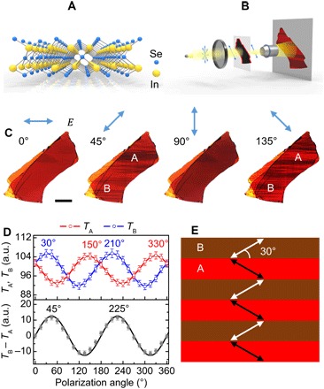
(A) Crystal structure of layered β-In2Se3. (B) Schematic of the linear polarization optical microscopy measurement. (C) Optical image sequence of β′-In2Se3 imaged by light of different polarization angles. Scale bar, 25 μm. (D) Polarization angle dependence of the light transmission of the regions A and B as shown in (C). a.u., arbitrary units. (E) Schematic of the optical axes of regions A and B.
Figure 1B shows a schematic of the experimental setup for imaging of the exfoliated β-In2Se3 using polarized light in transmission mode, and Fig. 1C shows a sequence of optical images of exfoliated β-In2Se3 with a thickness of ~100 nm illuminated with various linear polarization directions at RT. We define the horizontal direction as 0°. Surprisingly, the image reveals the presence of domains in the shape of long stripes that are not visible under unpolarized illumination. We denote the two types of domains as A and B. Figure 1D plots the transmitted light intensities from A and B as a function of the light polarization angle φ. We can see the transmission intensities from A and B oscillate with 180° periodicity, indicating linear dichroism in regions A and B (30, 31). Inspection of the top graph of Fig. 1D shows that the contrast arises because the optical axes of regions A and B are different, at 330° and 30°, respectively, with the angle difference of 60°. Examination of other β-In2Se3 flakes showed similar results. The domains always have optical axes differing by 60° or 120°. On the basis of these observations, we can explain the image contrast as follows. The transmission intensities TA of A and TB of B and their difference TB − TA are given by
| (1) |
| (2) |
| (3) |
where To is the based transmission intensity, ω is the transmission coefficient, and I is the incident light intensity. The factor of 2 in the equations is because there is no antiparallel direction between the polarization light and optical axis. In addition, in the above equations, we assume that the two domains have the same optical properties except their polar directions. The bottom graph of Fig. 1D plots TB − TA as a function of polarization angle of incident light, and the black curve is the fitting curve using Eq. 3. We can see that the contrast between A and B domains disappears at the light polarization angle of 0°, 90°, 180°, and 270° due to the linear dichroism of the domains. Figure 1E plots the schematic optical axes of A and B. The domain structure is very stable and remains the same even in a thin (45 nm) sample after 60-day ambient exposure (see fig. S2).
To further understand the properties of the domains, we applied LEEM and selected-area μ-LEED to investigate the surface of In2Se3. In our experiments, we obtained a fresh In2Se3 surface by cleaving large In2Se3 single crystals, followed by a brief thermal annealing at 100°C in ultrahigh vacuum (1 × 10⁻⁹ torr) (see Materials and Methods). Figure 2A shows the bright-field LEEM images of the In2Se3 surface at RT using a tilted electron beam (fig. S3). Different from the optical images shown in Fig. 1C, there are three types of domains, which are marked by blue, yellow, and green dots in Fig. 2A, respectively. Figure 2B presents the μ-LEED patterns of the three kinds of domains. As shown, the diffraction pattern of each domain contains a row of subspots, which subdivide the distance between two main spots, such as the (−1,0) and (0,−1) spots denoted in the bottom image of Fig. 2B, into nine equal parts along one of the three close-packed directions (see Fig. 2, B and C). Note that we cannot rule out whether there is another period, such as eighth, owing to the weak intensities of the subspots. The results suggest that each domain is formed by a 1D superlattice structure along any one of three equivalent close-packed directions of the hexagonal c plane. The diffraction patterns demonstrate that our In2Se3 sample belongs to the β′ phase, which has been discovered in electron diffraction experiments in the 1970s by cooling β-In2Se3 from 200°C (24).
Fig. 2. Low LEEM measurement.
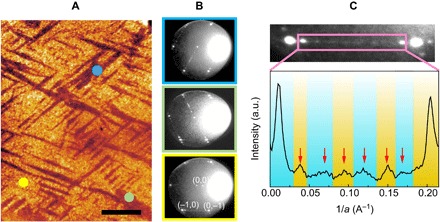
(A) Bright-field LEEM image of β′-In2Se3 surface taken by a tilted electron beam at 9.9 eV. Scale bar, 1.5 μm. (B) LEED patterns of the three domains. (C) Intensity profile of the subdiffraction spots between the (−1,0) and (0,−1) spots.
Using LEEM, we can shed more light on the β′ ↔ β phase transition through imaging in real time in both real and reciprocal space. We focus on one long stripe domain with uniform width, as shown in Fig. 3A. Figure 3B shows a number of LEEM images of the domain at different temperatures during the cycle of heating and cooling. From 42° to 190°C, the width of the domain only shrinks from 1.9 to 1.6 μm; the slight shrinkage indicates that the domain is stable over the temperature window. However, the width markedly decreases from 1.6 to 0.67 μm when the temperature increases from 190° to 195°C and, finally, the domain disappears at 204°C. Meanwhile, the μ-LEED pattern (Fig. 3D) taken from the surface at 204°C only indicates the Bragg spots of hexagon but no subspots of the superstructure, which still exist at 190°C (see Fig. 3C). Thus, both the real space and the diffraction patterns confirm the completion of the phase transition from β′ to β at 204°C (24).
Fig. 3. Curie temperature of β′-In2Se3.
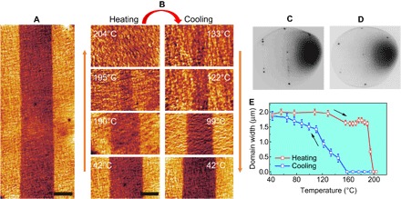
(A) LEEM image of a long-stripe domain in β′-In2Se3 at RT. (B) Shrinking and disappearance of domain as temperature increases and recovery of domain during cooling. (C) LEED pattern of β′-In2Se3 at 190°C. (D) LEED pattern of β-In2Se3 at 204°C. (E) Width of the domain as a function of temperature during heating and cooling. Scale bars, 1 μm (A and B).
Afterward, we start cooling the sample to investigate the recovery of the domains. The right column of Fig. 3B shows the results. The domain reappears at its previous location, with the onset temperature of the domain contrast at 145°C, much lower than that of the large domain shrinkage (195°C) during heating. As the temperature continues decreasing, the width of the domain grows gradually. Figure 3E shows the width of the domain as a function of temperature during the heating (red) and cooling (blue) processes. At each point in the figure, we stabilized the sample at the temperature for at least 10 min to achieve the equilibrium state of the domain. As shown, there is a large hysteresis loop of the phase transition between the heating and the cooling periods. The domain grows (shrinks) continuously during the cooling (heating) period near criticality. The continuous phase transition indicates that the β-to-β′ phase transition is of second order. Moreover, our LEEM experiments reveal that the dynamics of domain growth/shrinkage is highly anisotropic. The length of the domain grows much faster than the width. The anisotropic dynamics is possibly due to the 1D nature of the superstructure.
So far, the phase transition from β to β′ is still not fully addressed. In previous studies, it is generally believed that β′ phase was formed by cooling β-In2Se3 from 200°C and the phase exists in the temperature between 60° and 200°C (24, 32). Below 60°C, the β′ phase in the bulk crystals or thick layers of In2Se3 is thought to change to α phase with the disappearance of the superstructure (24). To date, the RT superstructures of the β′ phase were only observed in nanoribbons, nanowires, or monolayers of In2Se3 (32–34). However, our optical microscopy and LEEM experiments (Figs. 1 to 3) show that the β′ phase is stable at RT, both in thin layers and in bulk, and therefore suitable for electronic applications. The discrepancy might be due to the difference in crystal quality.
Previous studies speculated that the superstructures were due to a CDW state and the structural distortion was due to the freeze-in of a particular vibration mode (24). CDW formation is hard to reconcile with the semiconducting nature of β ′-In2Se3, and the electrical measurements carried out by other groups observed that the resistance of the β′ superstructure phase was significantly lower than that of the β phase, which is difficult to understand if the β′ phase is due to CDW formation (34, 35). The linear dichroism and the angle-dependent LEEM contrast of the domains (fig. S5) suggest instead that the β′ phase is polar, and we thus speculate that the β-to-β′ phase transition is a ferroelectric transition.
To examine whether there is ferroelectricity in β′-In2Se3, we applied PFM to scan the surface in air at RT. Figure 4A shows the atomic force microscopy (AFM) topographic image of a freshly cleaved In2Se3 surface. As expected for a vdW material, the surface is atomically flat over large areas, with the exception of a few extraneous particles. Figure 4 (B and C) indicates the PFM out-of-plane magnitude and phase images of β′-In2Se3 surface. We observe no vertical piezoelectric response signal across the surface, suggesting that the material does not exhibit measurable out-of-plane ferroelectricity. In contrast, the in-plane PFM magnitude image (Fig. 4D) and phase image (Fig. 4E) show a strong signal, with stripe domains similar to those observed in polarization microscopy and LEEM. These results verify the existence of in-plane ferroelectricity in In2Se3. In-plane ferroelectricity also explains the LEEM contrast mechanism, as seen in Fig. 2, as due to the polar structure. The disappearance of the LEEM contrast at the β′-to-β phase transition thus indicates that ferroelectricity is associated with the β′ phase, that is, the presence of the superlattice. On the basis of the linear dichroism and LEEM image contrast study, we can now plot the polarization direction of each domain (see Fig. 4F).
Fig. 4. PFM measurements.
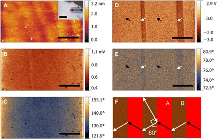
(A) AFM topography image of β′-In2Se3. Inset: Optical image of the cantilever and the exfoliated crystal. The horizontal scanning direction is indicated by the black double-headed arrow. (B and C) PFM amplitude and phase of vertical signal. (D and E) PFM amplitude and phase of lateral signal. (F) Schematic of the example optical axis (white double-headed arrow) and ferroelectric polarization directions (white/black arrows) of the domains. Scale bars, 5 and 30 μm (inset).
To attempt to resolve the atomic structure, we imaged the surface of In2Se3 using STM at 77 K. Figure 5A shows the large-scale STM image of β′-In2Se3 surface scanned at 77 K. Many dark depressions are evident on the surface, possibly pinholes in the crystal or defects due to imperfect cleaving. The STM image indicates the weak contrast of well-aligned stripes throughout the surface. According to the line profile taken from the rectangular region shown in Fig. 5A, the distance between the stripes is either 1.6 or 2 nm, which is equal to the length of 4 or 5 unit cells, respectively (see the inset of Fig. 5A). Similarly, a Fourier transform of the STM image (inset) shows well-defined spots corresponding to a real-space periodicity of 1.822 nm. The result suggests that the STM probes a periodicity that is half the periodicity seen in electron diffraction (Fig. 2), suggesting that the actual supercell consists of two of the rows imaged in STM. Figure 5B shows the zoomed-in STM image showing the positions of Se atoms of In2Se3 surface. The Se lattice is roughly triangular with a Se-Se distance of 0.4 nm, which is similar to the β phase. The 1D superlattice structure appears as an apparent height variation of Se atoms, although we cannot determine from the image whether this is due to an actual height variation or an electronic effect (variation in the local density of states). Figure 5C shows the high-magnification image of the 1D superstructure. By taking the line profile along the blue line, we can see the intermixing of stripes of four-atom and five-atom widths. We note that the sample was rapidly cooled from RT to 77 K upon insertion into the STM, so we cannot rule out the possibility that the β′ requires rapid quenching to be stabilized at 77 K. However, given that the distortion associated with β′-In2Se3 is apparently imaged by STM, we conclude that the β′ phase is at least metastable at 77 K. The transmission electron microscopy (TEM) observations confirm the same structure at RT (see fig. S7).
Fig. 5. STM measurements.
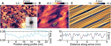
(A) Large-area STM image of β′-In2Se3 at 77 K. Scale bar, 10 nm. The bottom graph presents the height profile of 1D superstructures, and the inset indicates the fast Fourier transform pattern showing spots of the superstructures. (B) Zoomed-in STM image showing the atomic structure of unit cell and the 1D superstructures due to height modulation. Scale bar, 1 nm. (C) Atomic structure of 1D superstructures taken from another region. The bottom graph shows the height profile taken from the blue line. Scale bar, 1 nm.
The β phase appearing at >200°C belongs to 166 group, which owns inversion symmetry (24). The emergence of ferroelectricity requires the breaking of inversion symmetry. However, the detailed atomic displacements are not evident in electron diffraction or STM. More experimental work is required to determine the atomic structure.
We performed density functional theory (DFT) calculations to study the stability of the single unit cell of β-In2Se3. We started from the high-temperature phase, β. This structure has inversion symmetry and exhibits no ferroelectricity in our DFT calculations (see Fig. 6). We found that, by shifting the central Se atom along one of the threefold symmetry direction, the total energy values reduced by 0.27 eV per unit cell. Our calculation (fig. S8) shows a polarization of 0.199 C/m2 for this new structure (Fig. 6). The lower total energy of this polar structure indicates that it is more energetic favorable at low temperatures. The polarization direction also appears to be consistent with the β′ phase in the experiments. However, our single-unit-cell model is not a superlattice structure as the β′ phase. More experimental and simulation work are required to establish the relationship between crystal structure and ferroelectric polarization of In2Se3.
Fig. 6. DFT calculation.
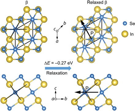
The top view (top) and the side view (bottom) of the β phase before and after relaxation, respectively. Ferroelectricity exists in a crystal structure relaxed from the β phase. The Se atoms in the middle of the five-atom layer shift along one of the threefold symmetry directions.
In summary, we have discovered RT in-plane ferroelectricity in vdW material β′-In2Se3 in bulk crystals and thin layers down to 45 nm. The β′-In2Se3 phase and superlattice structure are stable at RT, with a Curie temperature of up to 200°C. Because of the appearance of ferroelectric domains, In2Se3 shows linear dichroism. PFM confirms the existence of ferroelectric domains, and STM shows the 1D superstructure distortion of the atomic lattice. DFT confirms that β-In2Se3 is unstable to a ferroelectric distortion along the threefold high-symmetry directions. However, the exact structure of the large unit-cell superlattice distortion leading to ferroelectricity remains to be uncovered by further theoretical and experimental studies. Because of the difficulty in making large-area monolayer In2Se3 using exfoliation, we have not been able to confirm whether ferroelectricity persists to the monolayer limit. However, the observation of a similar superlattice structure in thin nanostructures of In2Se3 by others suggests that ferroelectricity is likely in ultrathin layers (33–35). We thus anticipate our results to open new possibilities of making multifunctional electronics of vdW materials coupling with in-plane ferroelectricity and linear dichroism of In2Se3.
MATERIALS AND METHODS
Linear dichroism measurement
A large single crystal of In2Se3 (HQ Graphene) was exfoliated using sticky tape (3M Scotch), and the flakes were deposited on polydimethylsiloxane substrates. The linear dichroism measurements were carried out using an optical microscope (Nikon Eclipse) with a linear polarizer. During measurements, the sample was fixed, and the polarization angle relative to the sample was changed by rotating the linear polarizer at steps of 15°. A 50× objective lens was used, and the charge-coupled device integration time was 1 ms.
LEEM measurement
The LEEM experiments were carried out on a SPECS FE-LEEM P90 with an aberration corrector. Clean In2Se3 was prepared by cleaving the large single crystals using sticky tape in ambient temperature, followed by a quick loading into the load lock chamber and pumping down to vacuum. Before the LEEM observation, the surface was briefly cleaned by annealing at 100°C for 2 hours and exposing to ultraviolet radiation for 15 min under ultrahigh vacuum (<10−9 torr). The tilted electron beam was necessary to observe the ferroelectric domains of In2Se3. Selected-area μ-LEED was applied to identify a single ferroelectric domain structure. Temperature-dependent phase transition was conducted under ultrahigh vacuum condition during imaging process.
PFM characterization
PFM measurement was carried out on a commercial AFM (Dimension Icon, Bruker) using a NanoScope V controller in near-contact resonance mode. During measurements, the Pt/Ir-coated conductive probes (SCM-PIT, Bruker) were driven at the frequency of ~340 kHz. To eliminate electrical charging effects, the samples were exfoliated and stuck to a conducting carbon tape.
STM measurement
STM images were obtained with a CreaTec LT-STM/AFM under ultrahigh vacuum (base pressure, <10−10 mbar) and a base temperature of 77 K.
DFT calculation
The Vienna ab initio simulation package (VASP v.5.3.3) was used to perform DFT calculations in this study (36). Projector augments wave method and the generalized gradient approximation were used (37, 38). A plane-wave cutoff energy was set to 600 eV. A Monkhorst-Pack k-points mesh of 13 × 13 × 3 was adopted for the unit cell (Fig. 1A). For the monolayer In2Se3, a thick vacuum layer was included to minimize interlayer interactions. An interlayer spacing of 24 Å was used throughout, which represents a good balance between computational accuracy and efforts. To hold this interlayer space constant, the VASP source code (constr_cell_relax.F) was modified to allow the cells to relax within the basal plane only. In all cases, the atomic positions were relaxed in all directions until the forces acting on each atom were below 0.005 eV A−1. To calculate the ferroelectric polarizations of the bulk In2Se3, the Berry phase method was applied (39).
Supplementary Material
Acknowledgments
Funding: C.Z. thanks the support from Australian Research Council (ARC) Discovery Early Career Researcher Award (DE140101555). M.S.F. acknowledges the support from ARC DP150103837. M.T.E. is funded by ARC DE160101157. C.X. and Y.Z. are supported by the Hong Kong Research Grants Council through the Early Career Scheme (project no. 25301617) and the Hong Kong Polytechnic University grant (project no. 1-ZE6G). J.S. acknowledges the support from ARC DP140102849. J.Z.L. and Y.L. acknowledge the high-performance computing facilities from the National Computational Infrastructure through the National Computational Merit Allocation Scheme scheme. W.-X.T. is financially supported by the National Natural Science Foundation of China as National Key Instrumental Development Scheme (no. A04-11227802), 985 Key National University Funding at Chongqing University (nos. 0211001104414 and 0211001104423), and Science and Technology Innovation Projects at Chongqing University (no. 0211005202084). J.L.C. acknowledges the support from the Monash Centre for Atomically Thin Materials and from ARC CE170100039. Y.Z. is supported by the National Nature Science Foundation of China (51702219). This work was performed, in part, at the Melbourne Centre for Nanofabrication in the Victorian Node of the Australian National Fabrication Facility. Author contributions: C.Z., W.-X.T., and M.S.F. conceived the project. C.Z., L.Y., L.Z., and M.L. collected the LEEM data. C.Z. and Y.Z. carried out the linear dichroism measurements. J.L.C. and M.T.E. obtained and analyzed the STM data. D.K. and J.S. worked on the PFM. Y.L. and J.Z.L. performed the DFT calculations. C.X. and Y.Z. carried out the TEM observation. C.Z., W.-X.T., and M.S.F. wrote the manuscript with input from all authors. Competing interests: The authors declare that they have no competing interests. Data and materials availability: All data needed to evaluate the conclusions in the paper are present in the paper and/or the Supplementary Materials. Additional data related to this paper may be requested from the authors.
SUPPLEMENTARY MATERIALS
Supplementary material for this article is available at http://advances.sciencemag.org/cgi/content/full/4/7/eaar7720/DC1
Fig. S1. X-ray diffraction spectrum of In2Se3 flakes.
Fig. S2. Air stability of In2Se3 and domains.
Fig. S3. Image contrast of domains under a tilted electron beam in LEEM.
Fig. S4. The control of electron beam tilt in LEEM.
Fig. S5. Tilt angle–dependent domain contrast.
Fig. S6. Proposed ferroelectric polarizations.
Fig. S7. TEM measurements.
Fig. S8. Ferroelectric polarization calculated using Berry phase method.
REFERENCES AND NOTES
- 1.Martin L. W., Rappe A. M., Thin-film ferroelectric materials and their applications. Nat. Rev. Mater. 2, 16087 (2016). [Google Scholar]
- 2.Belianinov A., He Q., Dziaugys A., Maksymovych P., Eliseev E., Borisevich A., Morozovska A., Banys J., Vysochanskii Y., Kalinin S. V., CuInP2S6 room temperature layered ferroelectric. Nano Lett. 15, 3808–3814 (2015). [DOI] [PubMed] [Google Scholar]
- 3.Chang K., Liu J., Lin H., Wang N., Zhao K., Zhang A., Jin F., Zhong Y., Hu X., Duan W., Zhang Q., Fu L., Xue Q.-K., Chen X., Ji S.-H., Discovery of robust in-plane ferroelectricity in atomic-thick SnTe. Science 353, 274–278 (2016). [DOI] [PubMed] [Google Scholar]
- 4.Ding W., Zhu J., Wang Z., Gao Y., Xiao D., Gu Y., Zhang Z., Zhu W., Prediction of intrinsic two-dimensional ferroelectrics in In2Se3 and other III2-VI3 van der Waals materials. Nat. Commun. 8, 14956 (2017). [DOI] [PMC free article] [PubMed] [Google Scholar]
- 5.Hu T., Wu H., Zeng H., Deng K., Kan E., New ferroelectric phase in atomic-thick phosphorene nanoribbons: Existence of in-plane electric polarization. Nano Lett. 16, 8015–8020 (2016). [DOI] [PubMed] [Google Scholar]
- 6.Liu F., You L., Seyler K. L., Li X., Yu P., Lin J., Wang X., Zhou J., Wang H., He H., Pantelides S. T., Zhou W., Sharma P., Xu X., Ajayan P. M., Wang J., Liu Z., Room-temperature ferroelectricity in CuInP2S6 ultrathin flakes. Nat. Commun. 7, 12357 (2016). [DOI] [PMC free article] [PubMed] [Google Scholar]
- 7.Geim A. K., Grigorieva I. V., Van der Waals heterostructures. Nature 499, 419–425 (2013). [DOI] [PubMed] [Google Scholar]
- 8.Dean C. R., Young A. F., Meric I., Lee C., Wang L., Sorgenfrei S., Watanabe K., Taniguchi T., Kim P., Shepard K. L., Hone J., Boron nitride substrates for high-quality graphene electronics. Nat. Nanotechnol. 5, 722–726 (2010). [DOI] [PubMed] [Google Scholar]
- 9.Wang J., Deng S., Liu Z., Liu Z., The rare two-dimensional materials with Dirac cones. Nat. Rev. Mater. 2, 22–39 (2015). [Google Scholar]
- 10.Wang Q. H., Kalantar-Zadeh K., Kis A., Coleman J. N., Strano M. S., Electronics and optoelectronics of two-dimensional transition metal dichalcogenides. Nat. Nanotechnol. 7, 699–712 (2012). [DOI] [PubMed] [Google Scholar]
- 11.Lu J. M., Zheliuk O., Leermakers I., Yuan N. F. Q., Zeitler U., Law K. T., Ye J. T., Evidence for two-dimensional Ising superconductivity in gated MoS2. Science 350, 1353–1357 (2015). [DOI] [PubMed] [Google Scholar]
- 12.Barja S., Wickenburg S., Liu Z.-F., Zhang Y., Ryu H., Ugeda M. M., Hussain Z., Shen Z.-X., Mo S.-K., Wong E., Salmeron M. B., Wang F., Crommie M. F., Ogletree D. F., Neaton J. B., Weber-Bargioni A., Charge density wave order in 1D mirror twin boundaries of single-layer MoSe2. Nat. Phys. 12, 751–756 (2016). [Google Scholar]
- 13.Wu W., Wang L., Li Y., Zhang F., Lin L., Niu S., Chenet D., Zhang X., Hao Y., Heinz T. F., Hone J., Wang Z. L., Piezoelectricity of single-atomic-layer MoS2 for energy conversion and piezotronics. Nature 514, 470–474 (2014). [DOI] [PubMed] [Google Scholar]
- 14.Gong C., Li L., Li Z., Ji H., Stern A., Xia Y., Cao T., Bao W., Wang C., Wang Y., Qiu Z. Q., Cava R. J., Louie S. G., Xia J., Zhang X., Discovery of intrinsic ferromagnetism in two-dimensional van der Waals crystals. Nature 546, 265–269 (2017). [DOI] [PubMed] [Google Scholar]
- 15.Zhou Y., Wu D., Zhu Y., Cho Y., He Q., Yang X., Herrera K., Chu Z., Han Y., Downer M., Peng H., Lai K., Out-of-plane piezoelectricity and ferroelectricity in layered α-In2Se3 nano-flakes. Nano Lett. 17, 5508–5513 (2017). [DOI] [PubMed] [Google Scholar]
- 16.Liao W.-Q., Zhang Y., Hu C.-L., Mao J.-G., Ye H.-Y., Li P.-F., Huang S. D., Xiong R.-G., A lead-halide perovskite molecular ferroelectric semiconductor. Nat. Commun. 6, 7338 (2015). [DOI] [PMC free article] [PubMed] [Google Scholar]
- 17.Fu D.-W., Cai H.-L., Liu Y., Ye Q., Zhang W., Zhang Y., Chen X.-Y., Giovannetti G., Capone M., Li J., Xiong R.-G., Diisopropylammonium bromide is a high-temperature molecular ferroelectric crystal. Science 339, 425–428 (2013). [DOI] [PubMed] [Google Scholar]
- 18.Wang H., Qian X., Two-dimensional multiferroics in monolayer group IV monochalcogenides. 2D Mater. 4, 015042 (2017). [Google Scholar]
- 19.Mehboudi M., Fregoso B. M., Yang Y., Zhu W., van der Zande A., Ferrer J., Bellaiche L., Kumar P., Barraza-Lopez S., Structural phase transition and material properties of few-layer monochalcogenides. Phys. Rev. Lett. 117, 246802 (2016). [DOI] [PubMed] [Google Scholar]
- 20.Fei R., Kang W., Yang L., Ferroelectricity and phase transitions in monolayer group-IV monochalcogenides. Phys. Rev. Lett. 117, 097601 (2016). [DOI] [PubMed] [Google Scholar]
- 21.Haleoot R., Paillard C., Kaloni T. P., Mehboudi M., Xu B., Bellaiche L., Barraza-Lopez S., Photostrictive two-dimensional materials in the monochalcogenide family. Phys. Rev. Lett. 118, 227401 (2017). [DOI] [PubMed] [Google Scholar]
- 22.Wu M., Zeng X. C., Intrinsic ferroelasticity and/or multiferroicity in two-dimensional phosphorene and phosphorene analogues. Nano Lett. 16, 3236–3241 (2016). [DOI] [PubMed] [Google Scholar]
- 23.Han G., Chen Z.-G., Drennan J., Zou J., Indium selenides: Structural characteristics, synthesis and their thermoelectric performances. Small 10, 2747–2765 (2014). [DOI] [PubMed] [Google Scholar]
- 24.van Landuyt J., van Tendeloo G., Amelinckx S., Phase transitions in In2Se3 as studied by electron microscopy and electron diffraction. Phys. Status Solidi A 30, 299–314 (1975). [Google Scholar]
- 25.Popović S., Čelustka B., Bidjin D., A remark on the paper “phase transitions in In2Se3 as studied by electron microscopy and electron diffraction”. Phys. Status Solidi A 33, K23–K24 (1976). [Google Scholar]
- 26.Cui C., Hu W.-J., Yan X., Addiego C., Gao W., Wang Y., Wang Z., Li L., Cheng Y., Li P., Zhang X., Alshareef H. N., Wu T., Zhu W., Pan X., Li L.-J., Intercorrelated in-plane and out-of-plane ferroelectricity in ultrathin two-dimensional layered semiconductor In2Se3. Nano Lett. 18, 1253–1258 (2018). [DOI] [PubMed] [Google Scholar]
- 27.Lee H., Kim Y. K., Kim D., Kang D.-H., Switching behavior of indium selenide-based phase-change memory cell. IEEE Trans. Magn. 41, 1034–1036 (2005). [Google Scholar]
- 28.Jacobs-Gedrim R. B., Shanmugam M., Jain N., Durcan C. A., Murphy M. T., Murray T. M., Matyi R. J., Moore R. L. II, Yu B., Extraordinary photoresponse in two-dimensional In2Se3 nanosheets. ACS Nano 8, 514–521 (2014). [DOI] [PubMed] [Google Scholar]
- 29.Likforman A., Fourcroy P.-H., Guittard M., Flahaut J., Poirier R., Szydlo N., Transitions de la forme de haute température α de In2Se3, de part et d’autre de la température ambiante. J. Solid State Chem. 33, 91–97 (1980). [Google Scholar]
- 30.Stöhr J., Padmore H. A., Anders S., Stammler T., Scheinfein M. R., Principles of x-ray magnetic dichroism spectromicroscopy. Surf. Rev. Lett. 05, 1297–1308 (1998). [Google Scholar]
- 31.Chopdekar R. V., Malik V. K., Fraile Rodríguez A., Le Guyader L., Takamura Y., Scholl A., Stender D., Schneider C. W., Bernhard C., Nolting F., Heyderman L. J., Spatially resolved strain-imprinted magnetic states in an artificial multiferroic. Phys. Rev. B 86, 014408 (2012). [Google Scholar]
- 32.Manolikas C., New results on the phase transformations of In2Se3. J. Solid State Chem. 74, 319–328 (1988). [Google Scholar]
- 33.Peng H., Schoen D. T., Meister S., Zhang X. F., Cui Y., Synthesis and phase transformation of In2Se3 and CuInSe2 nanowires. J. Am. Chem. Soc. 129, 34–35 (2007). [DOI] [PubMed] [Google Scholar]
- 34.Lai K., Peng H., Kundhikanjana W., Schoen D. T., Xie C., Meister S., Cui Y., Kelly M. A., Shen Z.-X., Nanoscale electronic inhomogeneity in In2Se3 nanoribbons revealed by microwave impedance microscopy. Nano Lett. 9, 1265–1269 (2009). [DOI] [PubMed] [Google Scholar]
- 35.Lin M., Wu D., Zhou Y., Huang W., Jiang W., Zheng W., Zhao S., Jin C., Guo Y., Peng H., Liu Z., Controlled growth of atomically thin In2Se3 flakes by van der Waals epitaxy. J. Am. Chem. Soc. 135, 13274–13277 (2013). [DOI] [PubMed] [Google Scholar]
- 36.Kresse G., Furthmüller J., Efficient iterative schemes for ab initio total-energy calculations using a plane-wave basis set. Phys. Rev. B 54, 11169–11186 (1996). [DOI] [PubMed] [Google Scholar]
- 37.Blöchl P. E., Projector augmented-wave method. Phys. Rev. B 50, 17953–17979 (1994). [DOI] [PubMed] [Google Scholar]
- 38.Kresse G., Joubert D., From ultrasoft pseudopotentials to the projector augmented-wave method. Phys. Rev. B 59, 1758–1775 (1999). [Google Scholar]
- 39.King-Smith R. D., Vanderbilt D., Theory of polarization of crystalline solids. Phys. Rev. B 47, 1651–1654 (1993). [DOI] [PubMed] [Google Scholar]
- 40.Bauer E., Low energy electron microscopy. Rep. Prog. Phys. 57, 895–938 (1994). [Google Scholar]
- 41.D. B. Williams, C. B. Carter, Transmission Electron Microscopy: A Textbook for Materials Science (Springer, ed. 2, 2009). [Google Scholar]
- 42.Cherifi S., Hertel R., Fusil S., Béa H., Bouzehouane K., Allibe J., Bibes M., Barthélémy A., Imaging ferroelectric domains in multiferroics using a low-energy electron microscope in the mirror operation mode. Phys. Status Solidi RRL 4, 22–24 (2010). [Google Scholar]
- 43.Nataf G. F., Grysan P., Guennou M., Kreisel J., Martinotti D., Rountree C. L., Mathieu C., Barrett N., Low energy electron imaging of domains and domain walls in magnesium-doped lithium niobate. Sci. Rep. 6, 33098 (2016). [DOI] [PMC free article] [PubMed] [Google Scholar]
- 44.Barrett N., Rault J. E., Wang J. L., Mathieu C., Locatelli A., Mentes T. O., Niño M. A., Fusil S., Bibes M., Barthélémy A., Sando D., Ren W., Prosandeev S., Bellaiche L., Vilquin B., Petraru A., Krug I. P., Schneider C. M., Full field electron spectromicroscopy applied to ferroelectric materials. J. Appl. Phys. 113, 187217 (2013). [Google Scholar]
- 45.Rault J. E., Menteş T. O., Locatelli A., Barrett N., Reversible switching of in-plane polarized ferroelectric domains in BaTiO3(001) with very low energy electrons. Sci. Rep. 4, 6792 (2014). [DOI] [PMC free article] [PubMed] [Google Scholar]
- 46.Balakrishnan N., Staddon C. R., Smith E. F., Stec J., Gay D., Mudd G. W., Makarovsky O., Kudrynskyi Z. R., Kovalyuk Z. D., Eaves L., Patanè A., Beton P. H., Quantum confinement and photoresponsivity of β-In2Se3 nanosheets grown by physical vapour transport. 2D Mater. 3, 025030 (2016). [Google Scholar]
- 47.Suzuki K., Kijima K., Optical band gap of barium titanate nanoparticles prepared by RF-plasma chemical vapor deposition. Jpn. J. Appl. Phys. 44, 2081–2082 (2005). [Google Scholar]
Associated Data
This section collects any data citations, data availability statements, or supplementary materials included in this article.
Supplementary Materials
Supplementary material for this article is available at http://advances.sciencemag.org/cgi/content/full/4/7/eaar7720/DC1
Fig. S1. X-ray diffraction spectrum of In2Se3 flakes.
Fig. S2. Air stability of In2Se3 and domains.
Fig. S3. Image contrast of domains under a tilted electron beam in LEEM.
Fig. S4. The control of electron beam tilt in LEEM.
Fig. S5. Tilt angle–dependent domain contrast.
Fig. S6. Proposed ferroelectric polarizations.
Fig. S7. TEM measurements.
Fig. S8. Ferroelectric polarization calculated using Berry phase method.


