Abstract
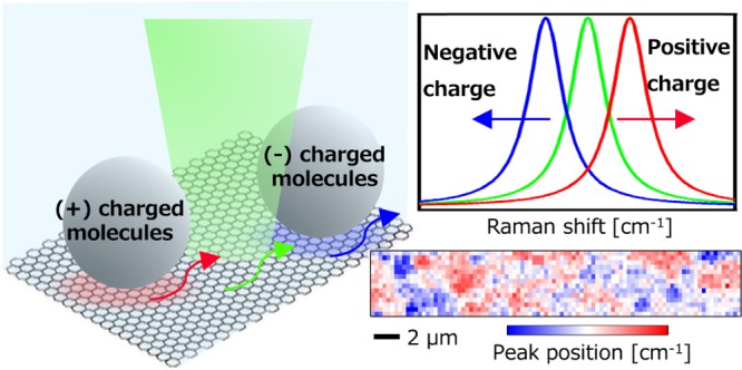
Graphene, a single atom layer of carbon atoms, provides a two-dimensional platform with an extremely high sensitivity to charges due to its unique band structure and high surface-to-volume ratio. Graphene field-effect transistor (G-FET) biosensors have, indeed, demonstrated a detection limit of subnanomolar or even subpicomolar. However, in G-FET, signal is averaged throughout the whole channel, so there remains a need to visualize the spatial distribution of target molecules on a single G-FET, to provide further insight into target molecules and/or biological functions. Here, we made use of graphene as an imaging platform of charged molecules via Raman microscopy. Positively (or negatively) charged microbeads with a diameter of 1 μm were dispersed in a buffer solution and were attached on graphene. We found out that Raman peaks of graphene, where positively (or negatively) charged beads contacted, were up-shifted (or down-shifted) significantly, indicating that the carrier density in the graphene was locally modulated by the charged beads and the charge state of the beads was represented by the peak-shift direction. From the peak shift, the change in the carrier density was calculated to be +1.4 × 1012 cm–2 (or −1.0 × 1012 cm–2). By taking Raman peak-shift images, we visualized distribution of charged molecules on graphene with a spatial resolution below 1 μm. The technique described here overcomes the limitation of spatial resolution of G-FET and provides a new route to graphene-based chemical and biosensors.
Introduction
Graphene, a two-dimensional (2D) sheet of hexagonally arranged carbon atoms, offers an ideal sensing platform owing to its 2D nature and its unique band structure. The 2D nature creates a uniform and large sensing field with ultrahigh sensitivity to charges because every atom in a graphene sheet makes contact with its environment. Therefore, even a few chemical dopants can lead to significant modulation of its carrier (electron or hole) density. In graphene field-effect transistor (G-FET) sensors, where graphene is used as a channel, a change in the carrier density is monitored as a drain current change. There have been reports on G-FET sensors showing successful detections of various gases,1 ions,2 biomolecules,3 and so on. However, in G-FET, the signal is averaged throughout the whole channel, so that spatial information of target molecules on G-FET cannot be obtained, and the signal is canceled out if both positively and negatively charged molecules are adsorbed in a single FET sensor. There are several methods to see local charge puddles in graphene with a high spatial resolution, including local potential Kelvin probe microscopy4 and scanning single-electron transistors.5 Here, we made use of graphene as an imaging platform of charged molecules via Raman microscopy. Raman microscopy is a noncontact, nondestructive, and label-free imaging technique with a spatial resolution below 1 μm and can be applied to samples in liquid environment, used to analyze biological materials,6 nanocarbon materials,7 polymers,8 and so on. Furthermore, it has been known that a change in the carrier density in graphene appears as distinct Raman peak shifts.9 Thus, by monitoring the peak shifts, local chemical dopants on graphene can be visualized via Raman microscopy. This method also enables one to investigate the charge state of biomolecules in liquid. Indeed, Paulus et al. have demonstrated a biological cell monitoring on graphene via Raman microscopy.10 We conducted our study with polystyrene (PS) beads of known ζ potential and demonstrated that a graphene imaging platform can visualize both positively and negatively charged molecules.
Results and Discussion
Analysis about Raman Images of Graphene Films under a Buffer Solution
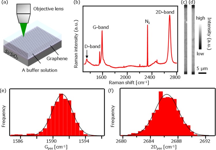
To ensure that graphene provides a uniform imaging platform in a liquid environment, we took Raman images of graphene films using Raman microscopy. The schematic experimental setup is depicted in Figure 1a. A phthalate buffer solution at pH = 4 (50 mM, Horiba) was dropped on graphene films. Figure 1b shows a typical Raman spectrum of graphene. The peak parameters are determined using the Lorentz function. The Raman spectrum shows distinctive peaks at 1591, 2686, and 1341 cm–1 assigned to G-band, 2D-band, and D-band of graphene, respectively. The peak at 2329 cm–1 is assigned to N2 in air, which does not disturb Raman analysis of graphene. The intensity ratio of the G-band to 2D-band (IG/I2D) and the full width at half-maximum of 2D-band (Γ2D) are calculated to be 0.64 and 29 cm–1, respectively. The symmetric Lorentzian line shape of the 2D-band indicates that the graphene films are a single layer.11Figure 1c,d shows Raman images constructed by IG and I2D, respectively. The Raman images clearly show that the obtained graphene films were uniform throughout the imaged area. To study more in detail, the Raman spectrum variance is investigated by making histograms of G-band peak position (Gpos) and 2D-band peak position (2Dpos; Figure 1e,f). The deviation in the peak positions was sufficiently small (<2 cm–1), which supports that the graphene provides a uniform imaging platform. The deviation is likely attributed to the inhomogeneous charged impurities in the SiO2 substrate.12
Figure 1.
(a) Schematic of setup for Raman measurement of graphene films immersed in a buffer solution. (b) A typical Raman spectrum of graphene showing G-band (1591 cm–1), 2D-band (2686 cm–1), and D-band (1341 cm–1) as well as N2 in air at 2329 cm–1. (c, d) Raman image of graphene constructed by IG (c) and I2D (d). The image is 10 × 184 pixels, where the pixel sizes are 205.2 nm in x and 214.2 nm in y directions. The scale bar is 5 μm. (e, f) Histograms of Gpos (e) and 2Dpos (f). Solid lines are Gaussian fitting curves for a guide to the eye.
To prove that Raman spectrum of graphene is sensitive to the carrier density change, we changed the carrier density by changing the pH of the buffer solution on graphene and investigated Raman spectrum of graphene. It is known that a pH change leads to a modulation of the carrier density of graphene.2 Raman images of the graphene films were taken at pH = 4 (phthalate buffer, 50 mM, Horiba), 7 (phosphate buffer, 25 mM, Horiba), and 9 (tetraborate buffer, 10 mM, Horiba). The averaged Raman spectra throughout the Raman images (see Figure S1 in the Supporting Information) are shown in Figure 2a–c. The results clearly show that both Gpos and 2Dpos are down-shifted with increasing pH. In contrast, no shift was observed at D-band and at the 2329 cm–1 peak assigned to N2, as expected. In addition to the peak position, the IG/I2D is also sensitive to the carrier density change. The IG/I2D as a function of pH is plotted in Figure 2d, showing that IG/I2D decreases with pH increase. The reliability was confirmed using Student’s t test with probability limits of p < 0.01. On the other hand, Γ2D did not show pH dependence, as shown in Figure 2e, because Γ2D is not sensitive to the carrier density change.13 Both the down shift of Gpos and 2Dpos and the decrease in IG/I2D are attributed to decrease in the carrier density in graphene.13 At high pH, deprotonated ions are adsorbed on graphene,2,14 which should lead to either increase in holes or decrease in electrons in graphene. As the Raman data indicate carrier density decrease at high pH, we concluded that the graphene films were n-doped in our system, where the graphene films were electrically floated under the buffer solution.
Figure 2.
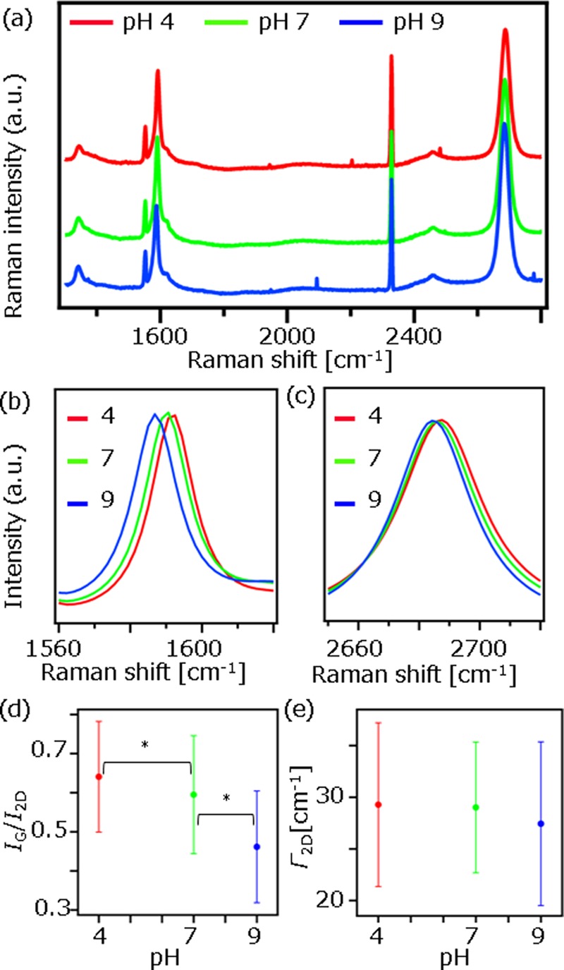
(a) Raman spectra of graphene taken at pH = 4 (red), 7 (green), and 9 (blue). (b, c) The enlarged spectra of G-band region (b) and 2D-band region (c) in (a). (d, e) IG/I2D (d) and Γ2D (e) as a function of pH. The asterisk in (d) indicates the values are statistically different (p < 0.01). Each point represents the average value throughout the Raman images (Figure S1). The error bar represents the standard deviation.
To provide further insights, we proved the reversible nature of the carrier density modulation by pH change. A buffer solution on the graphene films was replaced from pH = 4, 7, 9, 7, to 4, sequentially, and Raman images of the graphene films were taken at each condition (Figure S2). Figure 3 presents the transient response of the averaged Gpos against pH change. Averaged Gpos was calculated from the Raman images in Figure S2. The result shows that Gpos is monotonically down-shifted (up-shifted) with increasing (decreasing) pH, although there is a small offset shift probably due to insufficient rinsing such that some buffer solution residue remained. The validity was confirmed using Student’s t test with probability limit of p < 0.01. The tests show that the Gpos at different pHs is statistically different from each other. It is also found that 2Dpos is monotonically down-shifted with increasing pH (Figure S3). The sensitivity of 2Dpos against pH change is smaller than that of Gpos, in agreement with the previous report13 showing that 2Dpos against carrier density modulation is less sensitive compared to Gpos. Figure 3 also indicates that the Gpos instantly follows the pH change, which may lead to real-time monitoring of chemical dopants on graphene.
Figure 3.
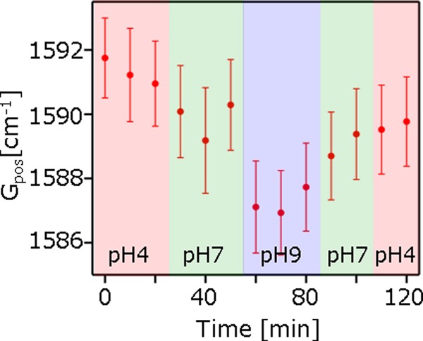
Transient response of Gpos against pH change. Each dot represents the average value from the Raman images in Figure S2. The error bar represents the standard deviation.
Visualization of Charged Molecular Distribution via Raman Imaging of Graphene Films
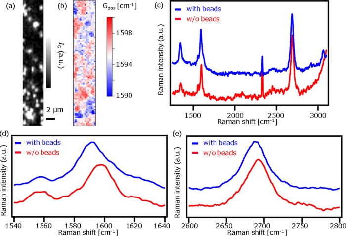
Finally, we demonstrated a detection of locally modulated carrier density via Raman microscopy using charged microbeads. Negatively charged polystyrene (PS) beads (1 μm diameter, surface density of COOH ∼2 × 1013 cm–2, micromod GmbH) were dispersed in a buffer solution at pH = 7. At pH = 7, the ζ potential of the beads was about −30 mV and thus were negatively charged in the solution. Figure 4a shows a Raman image constructed by IG. The PS beads were clearly observed as bright spots in Figure 4a, proving that our method has a high spatial resolution (down to 1 μm). The Raman image constructed by Gpos is also shown in Figure 4b. The image shows that Gpos where the PS beads are located is lower than that without PS beads. The down shift indicates that the negatively charged beads moved electrons away in the graphene, where beads were in contact. Typical Raman spectra taken from the area with and without casted PS beads are shown in Figure 4c. A peak at 3160 cm–1 is assigned to aromatic CH vibration in PS beads,15 confirming that Raman signal from the beads was detectable even on graphene. It is interesting to note that the intensity ratio of the G-band to D-band (IG/ID) with PS beads (∼1.64) was smaller than that without PS beads (∼2.67). This result also supports that the PS beads locally modulate carrier density in graphene, resulting in the local scatters. The averaged Gpos and 2Dpos with beads area are calculated to be 1594.7 and 2689.4, respectively, and the averaged Gpos and 2Dpos without beads area are calculated to be 1595.8 and 2690.3, respectively. Gpos is correlated to its electron density ne through eq 1(13,16)
| 1 |
where ΔGpos is the frequency shift from Gpos0 = 1581 cm–113 of graphene where ne is equal to hole density (nh) and νF = 1.1 × 10⁶ ms–1 is the Fermi velocity.17,18 By substituting ΔGpos in eq 1, the ne can be calculated to be 8.0 × 1012 cm–2 for graphene with beads and 9.0 × 1012 cm–2 without beads, yielding a decrease in ne of 1.0 × 1012 cm–2 by external potential of the beads. In addition to a decrease in ne, mechanical strain may also attribute to the peak shifts of Gpos and 2Dpos. According to the previous reports,13,19−21 the peaks were up-shifted along a slope of Δ2Dpos/ΔGpos = 2.2 under tensile strain and up-shifted along a slope of Δ2Dpos/ΔGpos = 0.2 under increase in ne. Therefore, the peak shifts (ΔGpos, Δ2Dpos) can be decomposed into the contribution of ne modulation and mechanical strain. It was found that the contribution of ne decrease to the peak shifts of (−1.1, −0.9 cm–1) was 69% and the rest was induced by compressive strain.
Figure 4.
(a, b) Raman images of the graphene films and negatively charged polystyrene (PS) beads constructed by IG (a) and Gpos (b). The scale bar is 2 μm. (c–e) Typical Raman spectra with beads (blue) and without beads (red) (c) and the enlarged spectra in G-band region (d) and 2D-band region (e).
To ensure that the peak shifts were truly caused by the charge of the beads, we carried out a control experiment using positively charged beads. Positively charged PS beads (1 μm diameter, surface density of NR3+ ∼ 2 × 1013 cm–2, micromod GmbH) were dispersed in a buffer solution at pH = 4, where the ζ potential of the beads was about +32 mV. Raman images constructed by IG and by Gpos are shown in Figure 5a,b. The image in Figure 5b shows that Gpos where the PS beads are located is higher than that without PS beads, as opposed to the data in Figure 4. The scatter plot in Figure 5c also clearly shows that both Gpos and 2Dpos are shifted toward high frequency with beads. From these results, we confirmed that the peak shifts were truly related to local increase/decrease in ne due to the charged beads. In addition, we can conclude that Raman microscopy can visualize the locally modulated ne of graphene. The averaged Gpos and 2Dpos with beads are calculated to be 1596.5 and 2691.6, respectively. Also, the averaged Gpos and 2Dpos without beads are calculated to be 1595.1 and 2689.1, respectively. Therefore, using eq 1, we found that the ne with beads was higher by 1.4 × 1012 cm–2 than that without beads. This value is close to that obtained using negatively charged beads, although the sign is opposite. This result is reasonable as the absolute values of the ζ potential of the beads are close with each other (−30 and +32 mV). The vector decomposition into mechanical strain and ne modulation was also applied for the peak shifts (1.4, 2.5 cm–1). It was found that the contribution of ne increase to the peak shifts was 20% and the rest was induced by tensile strain. The reason why the mechanical strain estimated from (ΔGpos, Δ2Dpos) was in opposite direction between positively and negatively charged beads may be due to the limited accuracy of Δ2Dpos, and this issue will be addressed in the future study.
Figure 5.
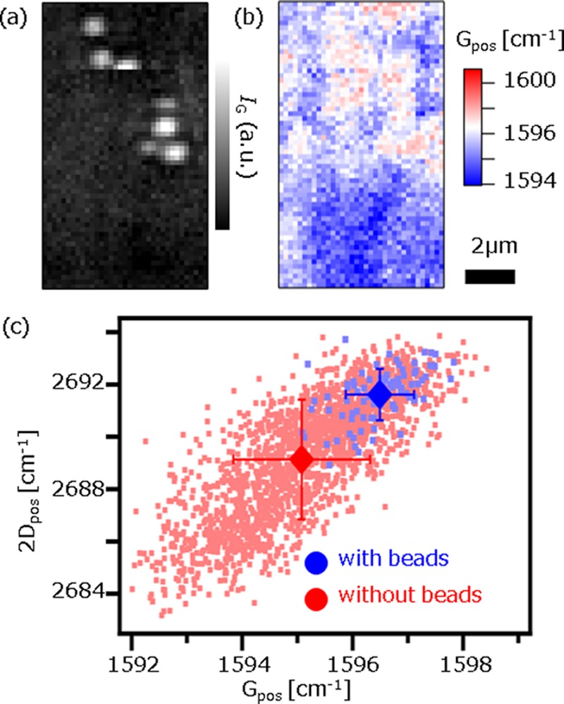
(a–c) Raman images of the graphene films and positively charged polystyrene (PS) beads constructed by IG (a) and Gpos (b). The scale bar is 2 μm. (c) Scatter plot of Gpos vs 2Dpos. The blue dots and the red dots represent the data from spectra with beads and without beads, respectively. The averaged Gpos and 2Dpos are also plotted as diamond marks in (c). The error bar represents standard deviation.
Conclusions
In conclusion, we have measured the ne change of graphene via Raman microscopy, using the 2D nature and high sensitivity of graphene. Both Gpos and 2Dpos shifted responding to changes in pH. We have also found the locally modulated ne by charged PS microbeads. The charged molecular distribution on graphene was imaged with a spatial resolution of submicrometer. The sensitivity relies on the Debye length in an analogous fashion of G-FET biosensors.22 We used buffer solutions of concentrations of 50 mM (pH = 4) and 25 mM (pH = 7), and so the Debye length is estimated to be 1 and 2 nm, respectively. This means that only charged molecules within the Debye length (<2 nm) will affect the local carrier density modulation, even though the diameter of the charged beads is 1 μm. Even in this condition, the results show that the Raman peaks were shifted by ∼1 cm–1, which represents that our method exhibits very high sensitivity. To further improve the sensitivity, some super-resolution techniques, including structured illumination Raman microscopy23 or tip-enhanced Raman microscopy,24 may be applied to our method. In addition, hexagonal boron nitride may be applied to suppress inhomogeneous charged impurities underneath graphene films,12 which may also lead to further enhancement in the sensitivity of our method. Because our method is a noncontact, nondestructive, and label-free measurement and is applicable to a liquid environment, it is possible to combine the system with G-FET biosensors, which will expand the application range of G-FET. Furthermore, although Raman spectroscopy generally provides no information regarding charge state of target molecules, we can find out qualitative information by putting them on a graphene imaging platform. Our technique described here, thus, opens the door to a more versatile sensing platform for biomolecules and biological functions.
Materials and Methods
Graphene films were grown on Cu foils by chemical vapor deposition. To transfer the graphene films to Si/SiO2 substrates, a poly(methyl methacrylate) (PMMA) solution was coated and subsequently the Cu foils were etched away using an ammonium persulfate solution. PMMA/graphene films were transferred onto Si/SiO2 substrates and finally PMMA was dissolved using acetone. The obtained graphene films were studied.
Raman analysis of graphene films was carried out using Raman microscopy (Raman-11, Nanophoton Corp.). A laser beam emitting at 532 nm was used for the excitation. The laser beam was focused by an objective lens (100×, NA 0.9, Nikon) onto the graphene films. The resolution of the spectrometer was about 4 cm–1 with the grating of 600 line/mm. It should be noted that the inaccuracy of determination of the peak position is much smaller than the resolution when the spectral shape is known. Laser intensity and exposure time were optimized to take Raman spectra with sufficient signal to noise ratio.
Acknowledgments
This work was supported by JST CREST Grant Number JPMJCR15F4, Japan.
Supporting Information Available
The Supporting Information is available free of charge on the ACS Publications website at DOI: 10.1021/acsomega.7b02008.
Details about Raman images of graphene films and pH-dependent Raman spectra and images of graphene (PDF)
Author Contributions
The manuscript was written through contributions of all authors. All authors have given approval to the final version of the manuscript.
The authors declare no competing financial interest.
Supplementary Material
References
- Schedin F.; Geim A.; Morozov S.; Hill E.; Blake P.; Katsnelson M.; Novoselov K. Detection of Individual Gas Molecules Adsorbed on Graphene. Nat. Mater. 2007, 6, 652–655. 10.1038/nmat1967. [DOI] [PubMed] [Google Scholar]
- Ohno Y.; Maehashi K.; Yamashiro Y.; Matsumoto K. Electrolyte-Gated Graphene Field-Effect Transistors for Detecting pH and Protein Adsorption. Nano Lett. 2009, 9, 3318–3322. 10.1021/nl901596m. [DOI] [PubMed] [Google Scholar]
- Ono T.; Oe T.; Kanai Y.; Ikuta T.; Ohno Y.; Maehashi K.; Inoue K.; Watanabe Y.; Nakakita S.; Suzuki Y.; et al. Glycan-Functionalized Graphene-FETs toward Selective Detection of Human-Infectious Avian Influenza Virus. Jpn. J. Appl. Phys. 2017, 56, 030302 10.7567/JJAP.56.030302. [DOI] [Google Scholar]
- Yan L.; Punckt C.; Aksay I.; Mertin W.; Bacher G. Local Voltage Drop in a Single Functionalized Graphene Sheet Characterized by Kelvin Probe Force Microscopy. Nano Lett. 2011, 11, 3543–3549. 10.1021/nl201070c. [DOI] [PubMed] [Google Scholar]
- Martin J.; Akerman N.; Ulbricht G.; Lohmann T.; Smet J.; Klitzing K.; Yacoby A. Observation of Electron–hole Puddles in Graphene Using a Scanning Single-Electron Transistor. Nat. Phys. 2007, 4, 144–148. 10.1038/nphys781. [DOI] [Google Scholar]
- Okada M.; Smith N.; Palonpon A.; Endo H.; Kawata S.; Sodeoka M.; Fujita K. Label-Free Raman Observation of Cytochrome c Dynamics during Apoptosis. Proc. Natl. Acad. Sci. U.S.A. 2012, 109, 28–32. 10.1073/pnas.1107524108. [DOI] [PMC free article] [PubMed] [Google Scholar]
- Ushiba S.; Shoji S.; Masui K.; Kuray P.; Kono J.; Kawata S. 3D Microfabrication of Single-Wall Carbon Nanotube/polymer Composites by Two-Photon Polymerization Lithography. Carbon 2013, 59, 283–288. 10.1016/j.carbon.2013.03.020. [DOI] [Google Scholar]
- Ushiba S.; Masui K.; Taguchi N.; Hamano T.; Kawata S.; Shoji S. Size dependent nanomechanics of coil spring shaped polymer nanowires. Sci. Rep. 2015, 5, 17152 10.1038/srep17152. [DOI] [PMC free article] [PubMed] [Google Scholar]
- Ryu S.; Liu L.; Berciaud S.; Yu Y.-J.; Liu H.; Kim P.; Flynn G.; Brus L. Atmospheric Oxygen Binding and Hole Doping in Deformed Graphene on a SiO2 Substrate. Nano Lett. 2010, 10, 4944–4951. 10.1021/nl1029607. [DOI] [PubMed] [Google Scholar]
- Paulus G.; Nelson J.; Lee K.; Wang Q.; Reuel N.; Grassbaugh B.; Kruss S.; Landry M.; Kang J.; Ende E.; et al. A Graphene-Based Physiometer Array for the Analysis of Single Biological Cells. Sci. Rep. 2014, 4, 6865 10.1038/srep06865. [DOI] [PMC free article] [PubMed] [Google Scholar]
- Malard L. M.; Pimenta M. A.; Dresselhaus; Dresselhaus Raman Spectroscopy in Graphene. Phys. Rep. 2009, 473, 51–87. 10.1016/j.physrep.2009.02.003. [DOI] [Google Scholar]
- Dean C. R.; Young A.; Meric I.; Lee C.; Wang L.; Sorgenfrei S.; Watanabe K.; Taniguchi T.; Kim P.; Shepard K.; et al. Boron Nitride Substrates for High-Quality Graphene Electronics. Nat. Nanotechnol. 2010, 5, 722–726. 10.1038/nnano.2010.172. [DOI] [PubMed] [Google Scholar]
- Froehlicher G.; Berciaud S. Raman Spectroscopy of Electrochemically Gated Graphene Transistors: Geometrical Capacitance, Electron-Phonon, Electron-Electron, and Electron-Defect Scattering. Phys. Rev. B 2015, 91, 205413 10.1103/PhysRevB.91.205413. [DOI] [Google Scholar]
- Yates D.; Levine S.; Healy T. Site-Binding Model of the Electrical Double Layer at the Oxide/water Interface. J. Chem. Soc., Faraday Trans. 1 1974, 70, 1807–1818. 10.1039/f19747001807. [DOI] [Google Scholar]
- Zumbusch A.; Holtom G.; Xie X. Three-Dimensional Vibrational Imaging by Coherent Anti-Stokes Raman Scattering. Phys. Rev. Lett. 1999, 82, 4142–4145. 10.1103/PhysRevLett.82.4142. [DOI] [Google Scholar]
- Das A.; Pisana S.; Chakraborty B.; Piscanec S.; Saha S.; Waghmare U.; Novoselov K.; Krishnamurthy H.; Geim A.; Ferrari A.; et al. Monitoring Dopants by Raman Scattering in an Electrochemically Top-Gated Graphene Transistor. Nat. Nanotechnol. 2008, 3, 210–215. 10.1038/nnano.2008.67. [DOI] [PubMed] [Google Scholar]
- Novoselov K. S.; Geim A. K.; Morozov S. V.; Jiang D.; Katsnelson M. I.; Grigorieva I. V.; Dubonos S. V.; Firsov A. A. Two-Dimensional Gas of Massless Dirac Fermions in Graphene. Nature 2005, 438, 197–200. 10.1038/nature04233. [DOI] [PubMed] [Google Scholar]
- Zhang Y.; Tan Y.-W.; Stormer H.; Kim P. Experimental Observation of the Quantum Hall Effect and Berry’s Phase in Graphene. Nature 2005, 438, 201–204. 10.1038/nature04235. [DOI] [PubMed] [Google Scholar]
- Mohiuddin T.; Lombardo A.; Nair R.; Bonetti A.; Savini G.; Jalil R.; Bonini N.; Basko D.; Galiotis C.; Marzari N.; et al. Uniaxial Strain in Graphene by Raman Spectroscopy: G Peak Splitting, Grüneisen Parameters, and Sample Orientation. Phys. Rev. B 2009, 79, 205433 10.1103/PhysRevB.79.205433. [DOI] [Google Scholar]
- Ding F.; Ji H.; Chen Y.; Herklotz A.; Dörr K.; Mei Y.; Rastelli A.; Schmidt O. Stretchable Graphene: A Close Look at Fundamental Parameters through Biaxial Straining. Nano Lett. 2010, 10, 3453–3458. 10.1021/nl101533x. [DOI] [PubMed] [Google Scholar]
- Lee J. E.; Ahn G.; Shim J.; Lee Y.; Ryu S. Optical Separation of Mechanical Strain from Charge Doping in Graphene. Nat. Commun. 2012, 3, 1024 10.1038/ncomms2022. [DOI] [PubMed] [Google Scholar]
- Ohno Y.; Maehashi K.; Matsumoto K. Label-Free Biosensors Based on Aptamer-Modified Graphene Field-Effect Transistors. J. Am. Chem. Soc. 2010, 132, 18012–18013. 10.1021/ja108127r. [DOI] [PubMed] [Google Scholar]
- Watanabe K.; Palonpon A.; Smith N.; Chiu L.; Kasai A.; Hashimoto H.; Kawata S.; Fujita K. Structured Line Illumination Raman Microscopy. Nat. Commun. 2015, 6, 10095 10.1038/ncomms10095. [DOI] [PMC free article] [PubMed] [Google Scholar]
- Yano T.-a.; Ichimura T.; Kuwahara S.; H’Dhili F.; Uetsuki K.; Okuno Y.; Verma P.; Kawata S. Tip-Enhanced Nano-Raman Analytical Imaging of Locally Induced Strain Distribution in Carbon Nanotubes. Nat. Commun. 2013, 4, 2592 10.1038/ncomms3592. [DOI] [PubMed] [Google Scholar]
Associated Data
This section collects any data citations, data availability statements, or supplementary materials included in this article.


