Abstract
We report a new hybrid integration scheme that offers for the first time a nanowire-on-lead approach, which enables independent electrical addressability, is scalable, and has superior spatial resolution in vertical nanowire arrays. The fabrication of these nanowire arrays is demonstrated to be scalable down to submicrometer site-to-site spacing and can be combined with standard integrated circuit fabrication technologies. We utilize these arrays to perform electrophysiological recordings from mouse and rat primary neurons and human induced pluripotent stem cell (hiPSC)-derived neurons, which revealed high signal-to-noise ratios and sensitivity to subthreshold postsynaptic potentials (PSPs). We measured electrical activity from rodent neurons from 8 days in vitro (DIV) to 14 DIV and from hiPSC-derived neurons at 6 weeks in vitro post culture with signal amplitudes up to 99 mV. Overall, our platform paves the way for longitudinal electrophysiological experiments on synaptic activity in human iPSC based disease models of neuronal networks, critical for understanding the mechanisms of neurological diseases and for developing drugs to treat them.
Keywords: Nanowire, neuron, intracellular, extracellular, subthreshold, drug-screening
Graphical Abstract
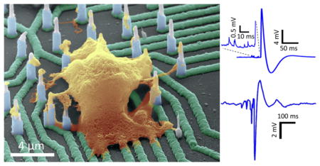
Nanowire geometries are ideal for interfacing with cells and measuring intracellular potentials of neurons with minimal invasiveness.1–6 Prior works have demonstrated single nanowire devices7,8 or devices encompassing ensembles of several nanowires,9–13 but individual electrical addressability of a single nanowire in a vertically standing array of nanowires, which is important for localizing the origin of action potentials, has not been accomplished before. Additionally, interfacing with human neurons, important for drug screening, is yet to be demonstrated. Here, we report a new hybrid integration scheme that offers for the first time a nanowire-on-lead approach, which enables independent electrical addressability, is scalable, has a high spatial resolution, and has a sensitivity that allows the detection of subthreshold PSPs. The fabrication of these nanowire arrays is demonstrated to be scalable down to submicrometer site-to-site spacing and can be combined with standard integrated circuit fabrication technologies. Physiological recordings from rodent primary neurons and human induced pluripotent stem cell (hiPSC)-derived neurons revealed high signal-to-noise ratios (SNRs) for both positive and negative measured potentials. We measured electrical activity from rodent neurons from 8 DIV to 14 DIV, and from hiPSC-derived neurons at 6 weeks in vitro post culture, and found intimate nanowire/neuron interaction validated by transmission electron microscopy (TEM). The technique contrasts to the standard patch-clamp,14–17 which is destructive and unscalable to large neuronal densities and to long recording times,18 or to planar multielectrode arrays that enable long-term recordings, but can just measure extracellular potentials and lack the sensitivity to subthreshold potentials.19
To measure minute potential changes in individual cells at high spatial resolution in neuronal networks, it is important to develop an integration scheme for high-density individually electrically addressable out-of-plane nanowire neuronal probes. To achieve very high densities of individual nanowires that are suitable for mapping individual units in neuronal networks, we devised a novel all solid-state wafer bonding integration scheme on patterned Ni electrical contacts and leads (Figure 1, Figures S1 and S2)20 leading to a superior high-density nanowire-neuron interface platform. This bonding scheme is essential because conventional low temperature eutectic bonding does not provide the lead-to-lead electrical isolation necessary for individual electrical addressability of single sites in a high-density nanowire array.21 Instead, we utilize the thermally driven solid-state diffusion of Ni into Si at a low temperature (400 °C), traditionally used to make self-aligned contacts for transistors in the semiconductor industry,22 to bond Si substrates to optically transparent and electrically insulating sapphire substrates that were predefined with Ni patterns. By doing so, we achieve two goals with the Ni layer: (1) bonding and fusion of a thin (~50 μm) Si substrate to the underlying host substrate and (2) embedding electrical leads underneath active or passive Si components in the bonded substrate with low contact resistance (Figure S1). The integration technique is general to any other substrate that can sustain the NiSi reaction temperature (starts at 300 °C), including complementary metal oxide semiconductor (CMOS) integrated circuits and advanced planar23,24 and out of plane device geometries are attainable through this method. Additionally, the optical transparency of sapphire enables light excitation and transmission imaging degrees of freedom in our platform. Overall, the integration technology developed in this work is the first to enable electrical addressability for individual vertically standing nanowires registered precisely over underlying metal leads. This individual electrical addressability of nanowires has potential to enable precise measurements of activity of individual units in neuronal networks, and to detect miniature release of neurotransmitters, especially important for investigating the synaptic properties of networks of neurons in the context of neurological diseases, as for the characterization of pre- or post- synaptic defects based on amplitude or frequency modifications in the subthreshold postsynaptic potentials.25,26
Figure 1.
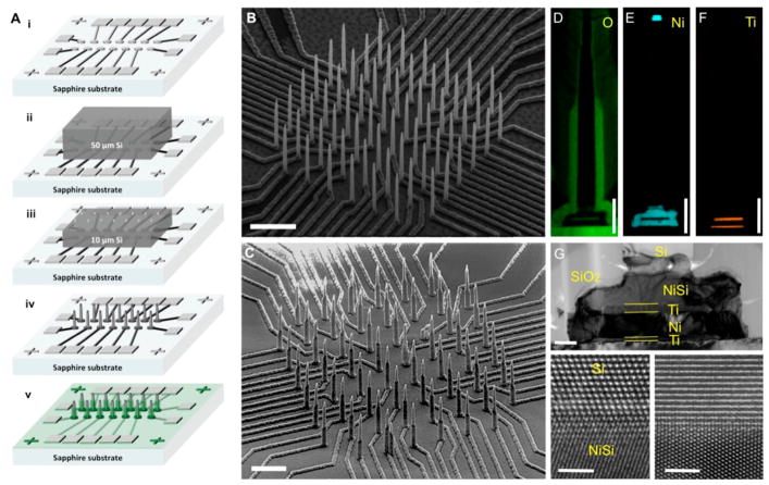
(A) Illustration of fabrication procedure for high density electrically isolated nanowire probes by solid-state wafer bonding. (i) Metal stack with Ni topmost layer is patterned by a combination of photolithography and electron beam lithography atop an electrically insulating and transparent sapphire substrate. (ii) Si is bonded to the substrate in i by nickel silicidation. (iii) Si wafer is thinned down to the desired wire height. Ni masks are then defined by electron beam lithography and aligned to the bottom plane Ni pattern. (iv) Si nanowires are etched by an SF6/C4F8 plasma etch step. (v) SiO2 PECVD is then deposited and is selectively etched to expose the tips of the Si nanowires. (B, C) SEM images of an 8 × 8 Si nanowire array (B) after etching and (C) after SiO2 passivation. Scale bar in B is 5 μm and in C is 3 μm. (D, E). Energy-dispersive X-ray spectroscopy (EDX) of the (D) oxygen signature of the SiO2 passivation layer, (E) nickel for etching mask (top), NiSi region, and conducting lower most layer, and (F) Ti as the diffusion barrier (top) and adhesion layer (bottom). Scale bars are 1 μm. (G) High magnification TEM image of the NiSi/Ti/Ni/Ti underneath the Si nanowire highlighting the interfacial structure between the bottom conducting lead and the Si nanowire. Scale bar is 200 nm. The bottom panels are HRTEM images at the interface between Si and NiSi with electron beam axis aligned in the Si [1̄10] (left panel), and the NiSi [1̄10] Zone axis in (right panel) to display the crystalline interface. Scale bars in bottom panels are 2 nm.
Fabrication of our in vitro platform starts with photolithography and e-beam lithography (EBL) patterning of electrode leads on a sapphire substrate, as shown schematically in Figure 1A–i.27 The electrode leads have metal stacking of Ti/Ni/Ti/Ni (30 nm/200 nm/50 nm/200 nm) for adhesion/conduction/diffusion-barrier/silicidation purposes, respectively. When a thin Si chip, 5 mm × 5 mm × 50 μm, is brought into contact with the metal leads on the sapphire substrate, a moderate heat treatment (400 °C) and compressive pressure (around 10 MPa) in a vacuum chamber with forming gas (H2 3–3.8% in N2) flow initiates a diffusion reaction between Ni and Si. The formed NiSi alloy fuses the two substrates together (Figure 1A–ii). The temperature 400 °C was chosen because it led to reacted NiSi leads that formed ohmic-like contacts with the heavily doped Si (Figures S1 and S2). The height of the desired nanowire array can be adjusted by an SF6 inductively coupled plasma (ICP) and reactive ion etch (RIE) that thins the Si substrate to around 8–10 μm (Figure 1A–iii). Another electron-beam lithography step patterns Ni etch mask dots aligned exactly at the tips of the Ni leads underneath the Si substrate (Figure 1A–iii). An SF6/C4F8 based ICP/RIE process is used to etch the Si everywhere except regions masked by the Ni dots, leaving vertically standing Si nanowires on NiSi leads (Figure 1A–iv and Figure 1B), which have diameters in the range of 100–200 nm in this work. To prevent electrochemical reactions anywhere except at the nanowire tips, the entire chip is coated by SiO2, which is then selectively etched at the contact pads and nanowire tips (Figure 1A–v, Figure 1C, Figure S4). The scanning electron microscope (SEM) images of the Si nanowire arrays in Figure 1B and C demonstrate a high packing density of 6.25Million/cm2 at a pitch of 4 μm. We also demonstrated submicrometer pitch at a site-to-site spacing of 750 nm (Figure S3). The array geometry can be tailored for the optimal growth of neuronal networks28 that are interconnected with sealed microfluidic channels that can allow growth of neurites and synaptic connections but prevent cell-body plating inside the channels (Figures S5 and S6). The electrochemical impedance in all of these configurations is relatively uniform (Figure S5 and S6) and validated a capacitively dominant coupling behavior (phase in Figure S7) with neuronal activity.
Transmission electron microscopy (TEM) and elemental mapping by energy-dispersive X-ray spectroscopy (EDX) of the Si nanowires demonstrate crystalline structures and interfaces and highlight the usefulness of each layer: Si constitutes the main body of the sensor, SiO2 constitutes the passivation outermost cylinder around the bottom portion of the nanowire (Figure 1D), Ni is used for silicidation bonding and as a current conduction layer (Figure 1E top and bottom, respectively), and Ti is used as a Ni diffusion barrier and adhesion layer (Figure 1F top and bottom, respectively). A zoomed-in TEM image at the bottom of the wire in Figure 1G highlights the interfacial layers crucial for the free-standing and individually electrically addressable nature of the Si nanowire. The high-resolution TEM (HRTEM) images in the lower panels of Figure 1G illustrate the crystalline nature of the interface between NiSi and Si at the bottom of the wire (see also Figure S9). Similar bonding structure, morphology, and interfaces were validated on SiO2/Si substrates (Figure S10) illustrating the versatility of our bonding scheme.
We next investigated the biological interfaces established between our Si nanowires and neurons and the resulting recorded electrophysiological activity. We packaged our devices on commercial electrophysiology printed circuit boards (Figure S8) and tested their feasibility for electrophysiology and pharmacology using rodent hippocampal primary neurons and human iPSC-derived neurons (Supporting Information sections 3 and 4). For both rodent primary and hiPSC-derived neurons, we find strong interaction between neurons and nanowires characterized by cell outgrowth and engulfment to the vertical Si nanowires (Figure 2A and Figure 4A, primary mouse neurons; Figure S12 uncolored SEM images). The cell-electrode interface is generally established in intracellular and extracellular configurations both of which can provide sufficient coupling between the cell and the electrode to enable high fidelity recordings.
Figure 2.
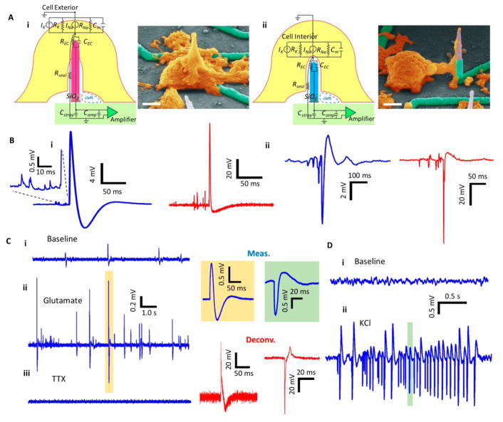
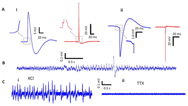
Modeling/characterization/measurement of the electro-neural system on mouse hippocampal neurons. (A) Electrical circuit models and corresponding SEM images of the electrode-cell engulfment. (i) Intracellular electrode configuration. (ii) Extracellular electrode configuration. The electrical circuit model of the electro-neural system starts by the cell culture (yellow) interfacing with the electrode, all the way to the read-out electronics represented by the amplifier block (green). INa and IK represents the Na+ and K+ ionic currents, and RNa and RK are the corresponding ion channel resistances. Rseal is the seal resistance at the cell-nanowire interface. REC represents the resistance of the electrochemical reaction at the electrode tip, and CEC is the double layer capacitance. Cstray and Camp are the bare electrode wire and amplifier’s input parasitic capacitances, respectively. (B) Spontaneous action potentials recorded on mouse hippocampal neurons. (i) Recordings showing the positive measured signal (~20 mV p-p) (left in blue) and after deconvolution (right in red). (ii) Recordings showing the negative measured signal (~10 mV p-p). Small potential fluctuations were captured in both cases. (C) Effect of external application of glutamate/TTX to the recordingsolution. (i) Baseline recordings showing the normal cell firing activity. (ii) After addition of 196 μM Glutamate to the recording solution, increased activity is observed. A sample action potential is shown on the right (blue), and its deconvoluted potential is shown below (red). (iii) After the application of 1.5 μM TTX, the cell activity is blocked. (D) Effect of addition of 13.2 mM KCl to the recording solution (i) Baseline recording showing very quiet cell activity. (ii) Following the application of KCl, increased cell activity was observed with a train of action potentials. Similarly, sample action potential is shown on the left (blue), and its deconvolution is shown below (red). Electrophysiology was performed at 8 DIV.
Figure 4.
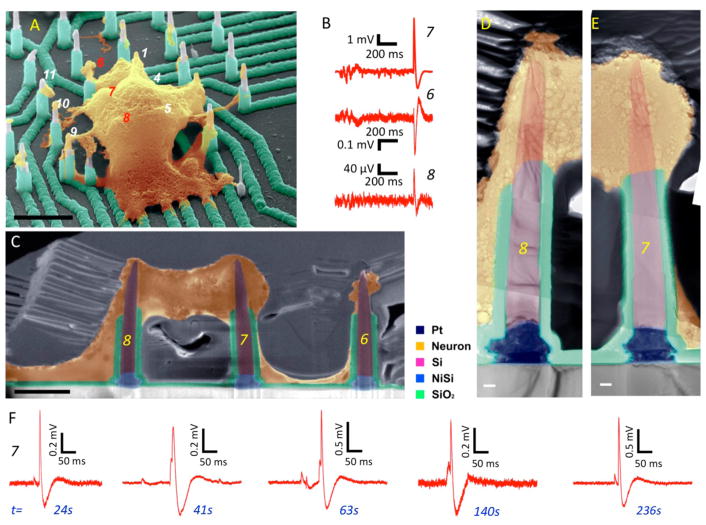
Recording from hiPSC-derived cortical neurons. (A) Colorized angle-view SEM image showing cell morphology and neurite outgrowth to nearby nanowires. Scale bar is 4 μm. (B) Measured potentials on channels 6–8 showing positive potentials for wires 7 and 8 inside the cell and negative potential for wire 6 outside the cell. (C) Colorized SEM image of the Pt coated and FIB thinned cross-section of the cell in panel B. The image shows the cell (yellow colored) engulfing the tops of nanowires 7 and 8, and portions of cell membrane around nanowire 6. Scale bar is 2 μm. Electrophysiology was performed 6 weeks post in vitro culture. (D, E) Higher magnification colorized TEM images collected and stacked to provide a higher resolution close-up to the nanowire-cell interface. The slight bending of the nanowires is likely to have happened during neuron dehydration in preparation for SEM imaging (section 5 of Supporting Information). Scale bars are 200 nm. (F) Recordings on nanowire number 7 illustrating consistent oscillations prior to action potential firing at different recording times.
The amplitude and shape of recorded potentials are governed by the electrochemical interface at the surface of the nanowire and the degree of sealing for the cell membrane to the nanowire itself, and by the measurement system.29–31 To account for these effects in both intracellular and extracellular configurations (Figure 2A), we developed a circuit model based on experimental measurements for each component of the electrode/neuron interface (see Supporting Information section 6). Results using analytic transfer functions, circuit simulations, and empirical transfer functions for the overall measurement system provided excellent agreement with the measured potentials.
One of the main signatures of our model is the use of current source and different conductance for the Na+ and K+ channels that is commensurate to the physical origin of the faster depolarization and repolarization in action potentials. These were calibrated to patch-clamp measured inward and outward ionic currents from similar cultured cells (Figure S15a). The longer duration of the patch-clamp action potentials has been previously related to maturity, culture conditions, and exact temperature of the cell culture for both hiPSC32 and rodent cortical neurons,33 which was also observed in our reference patch-clamp measurements (Figure S15a). Our electrophysiological models using either analog circuit analysis or empirical simulations based on detailed electrochemical characterization, similar to the models of Spira et al.29–31 are self-consistent models that can accurately reproduce both the time and the amplitude of deconvoluted neuronal signals measured from nanowires.
Pharmacological stimulation and inhibition validated the physiological origin of the measured potentials. After glutamate was added to the recording solution, we observed an increase of the cell spontaneous activity (Figure 2C–ii) with respect to frequency and amplitude when compared to the baseline (Figure 2C–i) measured on the same channel. The bath application of tetrodotoxin (TTX) inhibited the activity on the same channel (Figure 2C–iii). Similarly, for the extracellular configuration, the bath application of KCl led to increased activity (Figure 2D–ii) relative to the baseline recording (Figure 2D–i), which was also eliminated by TTX treatment.
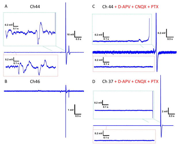
Strikingly, physiological measurements on mouse hippocampal neurons cultured for 10–13 days on our platform displayed small potential fluctuations prior to the positive (Figure 2B–i) and negative (Figure 2B–ii) firing events. The SNR of these prespike potentials is 20-times as evident in the inset of Figure 2B–i, and their shape is clearly different from coupled action potentials from different cells or channels. The largest action potentials that we measured 10 DIV is 99 mV, as shown in Figure 3A, which demonstrates for the first time that nanowires can measure intracellular potentials with similar magnitudes to that of patch-clamp. We generally observed oscillations prior to spikes as highlighted in the insets of Figure 3A. For a simultaneously measured extracellular potential from another channel (Figure 3B) that is 5.65 μm apart from the intracellular channel, we also observed potential oscillations prior to the extracellular spike. Upon inspecting all other channels, we did not observe action potentials that might be electronically coupled to these two channels. We then embarked on validating that these potential oscillations are subthreshold synaptic potentials. To do so, we pharmacologically blocked both excitatory and inhibitory receptors by adding D-APV to block NMDA receptors, CNQX for blocking AMPA receptors, and Picrotoxin for preventing the binding of the inhibitory neurotransmitter GABA to its receptors (see Supporting Information section 4 (1)). After adding the blockers, we observed insignificant number of small prespike oscillations (Figure 3C) or no oscillations (Figure 3D), which suggested that our system has the sensitivity to detect miniature release of neurotransmitters at a quantal level. Given that our nanowires can sometimes measure intracellular potentials with an SNR of 1700 (Figure 3A), it is not surprising that they can also resolve subthreshold activity that we validate with standard pharmacological experiments here. This can be attributed to the height of our nanowires, which is >6.5 μm compared to the shorter than 2 μm nanowires in prior works, providing larger Si surface interaction area with adherent neurons.
Figure 3.
Recording of a 99 mV action potential and pharmacological experiments for validating subthreshold potentials at 10 DIV. (A) Spontaneous activity measured on channel 44 showing subthreshold oscillations that are illustrated in the insets of a 1 s time window at the beginning of the trace (lower inset) and just at the action potential generation (top inset). (B) Concurrent recording with A from a nearby channel 46 showing some potential oscillations and negative spikes that occur simultaneously with those in A. (C) Recording with a solution containing D-APV (50 μM), CNQX (10 μM), and PTX (1 mM) to block NMDA, AMPA, and GABA receptors, respectively, shows a single oscillation prior to the spike on the same channel as in A. (D) Same in C from channel 37 showing no oscillations prior to the large action potential.
The development of high-throughput, subcellular neurotechnologies has the potential for application to drug screening on neurological disease models. We therefore tested the sensitivity of our platform with two clinically relevant subtypes of human iPSC-derived neurons, cortical and dopaminergic, for which we had demonstrated electrical activity on conventional microelectrode array recordings (Figure S11).
Human iPSC-derived cortical neurons cultured on our platform overlapped with multiple nanowires (Figure 4A). Post preparation for SEM on this platform, evidence of neurite outgrowth to nearby nanowires, is also apparent in Figure 4A. Nanowires 7 and 8 displayed positive action potentials, whereas nanowire 6 displayed a negative action potential (Figure 4B). From the SEM image of Figure 4A, we can note the extracellular nature of the interface with nanowire 6. To uncover the nature of the nanowire/neuron interaction for nanowires 7 and 8, we performed a sequential focused ion beam (FIB) cut and thinning of a 300–400 nm slice on the sample in regions of wires marked 6, 7, 8 (Figures S17–S21) post Pt plating. The sample is thin enough to allow electron transmission for TEM characterization without risking significant damage to the cell body during the FIB milling process. Figure 4C shows an SEM image of the FIB slice showing a clear dark contrast of the cell around nanowires 7 and 8. The TEM images in Figures 3D and 4E along the substrate-nanowire-cell regions demonstrated that the nano-wires displayed intimate interaction with neurons that is not aided by tension due to neuron adhesion and spreading on the substrate surface or peptide-modification,34–36 nor assisted with the highly invasive electroporation.9,10 The continuity of the inclined interface below the SiO2 passivation layer as seen to the right of the nanowires in Figure 4D and E is suggestive of intracellular penetration of the nanowires into the human cortical neuron cell body, which is commensurate with the positive potentials measured with wires 7 and 8.37 However, it is also possible that the cell fixation and FIB thinning can lead to artifacts in the observed interface. Also in these recordings, we observed the prespike potentials with sharp rise and slow decay times, which are similar in shape to the excitatory postsynaptic potentials (EPSPs) observed by Hai et al. using Au mushroom electrodes.38 It is possible however that the positive potentials are measured in a juxtacellular configuration due to their smaller amplitude than those observed in Figures 2, 3, and 5 since we did not validate their nature by blocking the postsynaptic receptors. We note that out of the two hiPSC cells on top of the nanowire array (Figure S17), we measured positive potentials from one neuron. The individually addressable nanowires can record multiple positive potentials from a single neuron.
Figure 5.
Recording from hiPSC-derived dopaminergic neurons 6 weeks post in vitro culture. (A) Spontaneous action potentials. (i) Positive potential recordings showing the measured signal (~30 mV p-p) (left in blue) and after deconvolution (right in red). (ii) Negative potential recordings (~6 mV p-p) (left in blue) and after deconvolution (right in red). (B) Potential oscillations recorded prior to action potential firing. (C) Effect of external application of stimulating/inhibiting media. (i) Increase of action potential firing following 13.2 mM KCl bath application. (ii) Increased activity abolished after the application of 1 μM TTX.
Dopaminergic neurons are a clinically relevant cell type for study of neurodegenerative disease and neuropsychiatric disorders. We determined whether hiPSC-derived dopaminergic neurons could also survive and demonstrate physiological function on our nanowire device. Six weeks postplating hiPSC-derived dopaminergic neurons on the nanowire platform, we observed distinctive single slope rise potentials compared to the multioscillation behavior exhibited by the mouse hippocampal neurons and hiPSC-derived cortical neurons prior to spontaneous action potential firing for both positive and negative polarities (inset, Figure 5A). On some channels, we observed small potential oscillations with varying frequency and amplitude as shown Figure 5B. We then performed pharmacological studies after 2 weeks postastrocyte coculture on the hiPSC-derived dopaminergic neurons (6 weeks post initial culture). Upon bath application of KCl, the firing rate increased and then all activity stopped after the addition of TTX as shown in Figure 5C. In conclusion, hiPSC-derived neurons not only survived several weeks intimately interfaced with the nanowires, but also we observed extensive electro-physiological activity over time, which led to the possibility of longitudinal electrophysiological experiments on synaptic activity on in vitro human neuronal networks.
The electrophysiological recordings from our cultures did not display trains of large action potentials, but just one or two APs, which is consistent with recordings from immature neurons and network observed on both human and rodent cultures from other groups.32,39 Therefore, we performed immunocytochemistry analyses on primary neurons cultured on our platform. The rat cortical neurons fixed at 15 DIV showed that the cells are well adherent to the nanowire arrays, stained positive for Tuj1, a specific neuronal marker, with some limited neurite extension. (Figure S22). The normal formation of a mature neuronal network can be compromised by the height of our nanowires that pin the cells above the planar regions of the platform. This can be improved by creating 3D islands at the bottom of the nanowires that can promote network connectivity on a 3D surface. In the extreme case of shortening the nanowires to heights that are similar to that is reported previously, the intracellular capability of the nanowires might be compromised. Increasing the spacing between the nanowires may also strengthen the network activity of the culture as noted in the recent work of Shmoel et al.40 but will compromise their density. Further investigation of the limited neurite extension in our cell culture will lead to improved network synaptic connections and to more robust and consistent measurements of action potentials and PSPs. (Figures 2–4).
It is also important to report the our primary rodent neuron experiments were conducted on 5 devices with successful measurements for several days for both intracellular-like and extracellular-like potentials on 4 out of the 5 devices. The measured intracellular-like potentials varied from 0.1 mV to 99 mV. The hiPSC experiments were conducted on 4 devices with successful measurements for several days for both intracellular-like and extracellular-like potentials on 4 out of the 5 sets, and for one device over several weeks (4 weeks and then 6 weeks after culture). The measured intracellular-like potentials varied from 0.1 mV to 35 mV. From Figure S17, we can observe 2 cells in the 28 μm × 28 μm square array of nanowires leading to a cell density of ~255 100 cells/cm2. One can also observe from Figure S17 that two out of the 12 nanowires in contact with the cultured cells resulted in intracellular-like measurements. As observed by other groups the variability of the Amplitude and duration of APs can be due to different engulfment level or cleft width between the neuron and the nanowire.40 The yield on nanowire internalization to cells can also be improved, for example with peptide modification.36
Measurement of intracellular action potentials using individually addressable Si nanowire probes, from both mouse and human neurons, opens new prospects on mapping neuronal activity in large networks, while the sensitivity to subthreshold postsynaptic potentials from multiple neurons opens new possibilities to study synaptic transmission mechanisms and plasticity, particularly important for investigating neurological diseases. Given the scalability of our arrays, the simultaneous recording of minute changes in cell potentials can uncover details on the synthesis, processing, and execution of neuronal network activity. In vitro, highly parallel drug screening experiments can be performed using the human relevant iPSC cell line and without the need of the laborious nonscalable patch-clamp. In vivo, targeted modulation of individual neural circuits or even single cells within a network becomes possible, and implications for bridging or repairing networks in neurologically affected regions become within reach. Overall, our platform and modified versions thereof have the potential to lead to transformative technologies for both in vivo and in vitro applications.
Supplementary Material
Acknowledgments
S.A.D. acknowledges support of the National Science Foundation under CAREER Program No. ECCS-1351980, which funded most aspects of this work. S.A.D. acknowledges support for efforts in this work under NSF DMR-1503595, the Center for Brain Activity Mapping at UC San Diego, a Qualcomm Institute CSRO Award CITD137, and a Laboratory Directed Research and Development Exploratory Research (LDRD-ER) award to S.A.D. from Los Alamos National Laboratory. Y.Z. acknowledges support of NIH R21 MH099082, March of Dimes award, and Frontiers of Innovation Scholars Program (FISP) to J.S. The work was performed in part at the Center for Integrated Nano-technologies (CINT), U.S. Department of Energy, Office of Basic Energy Sciences User Facility at Los Alamos National Laboratory (Contract No. DE-AC52-06NA25396), and Sandia National Laboratories (Contract No. DE-AC04-94AL85000). We are grateful for technical support from the nano3 clean room facilities at UC San Diego’s Qualcomm Institute and from the Integration Laboratory at CINT.
Footnotes
Author Contributions
S.A.D. conceived the integration scheme and platform design, led the project, wrote the manuscript, and received input from all coauthors. R.L., R.C., Y.H., A.T., Y.G.R., X.D., and S.A.D. fabricated the platform with input and equipment training from C.S., A.J., J.N., and D.B.W. R.L. performed the FIB sectioning and TEM characterization with input from D.V.P. and K.L.J.; J.S., S.H.L., and Y.Z. cultured the primary rodent neurons, and R.L., S.H.L., M.L.K., D.P., and S.A.D. performed electro-physiology on these devices. S.H., S.B., and A.G.B. performed the hiPSC culture and MEA analyses, and S.H.L, S.H., M.L.K., and A.K.M. performed electrophysiology on the hiPSC devices. A.T.E. and S.A.D. carried out the electrochemical interface modeling.
Notes
The authors declare no competing financial interest.
The Supporting Information is available free of charge on the ACS Publications website at DOI: 10.1021/acs.nano-lett.6b04752.
Detailed information regarding fabrication, packaging, electrochemical impedance spectroscopy, TEM sample preparation, cell culture, pharmacological stimulation and inhibition, SEM imaging, modeling and simulation, and nanowire-cell interface characterization (PDF)
References
- 1.Kim W, Ng JK, Kunitake ME, Conklin BR, Yang P. Interfacing silicon nanowires with mammalian cells. J Am Chem Soc. 2007;129(23):7228–7229. doi: 10.1021/ja071456k. [DOI] [PubMed] [Google Scholar]
- 2.Piret G, Perez M-T, Prinz CN. Neurite outgrowth and synaptophysin expression of postnatal CNS neurons on GaP nanowire arrays in long-term retinal cell culture. Biomaterials. 2013;34(4):875–887. doi: 10.1016/j.biomaterials.2012.10.042. [DOI] [PubMed] [Google Scholar]
- 3.Hanson L, Lin ZC, Xie C, Cui Y, Cui B. Characterization of the cell-nanopillar interface by transmission electron microscopy. Nano Lett. 2012;12(11):5815–5820. doi: 10.1021/nl303163y. [DOI] [PubMed] [Google Scholar]
- 4.Gällentoft L, Pettersson LM, Danielsen N, Schouenborg J, Prinz CN, Linsmeier CE. Size-dependent long-term tissue response to biostable nanowires in the brain. Biomaterials. 2015;42:172–183. doi: 10.1016/j.biomaterials.2014.11.051. [DOI] [PubMed] [Google Scholar]
- 5.Patolsky F, Timko BP, Yu G, Fang Y, Greytak AB, Zheng G, Lieber CM. Detection, stimulation, and inhibition of neuronal signals with high-density nanowire transistor arrays. Science. 2006;313(5790):1100–1104. doi: 10.1126/science.1128640. [DOI] [PubMed] [Google Scholar]
- 6.Cohen-Karni T, Qing Q, Li Q, Fang Y, Lieber CM. Graphene and nanowire transistors for cellular interfaces and electrical recording. Nano Lett. 2010;10(3):1098–1102. doi: 10.1021/nl1002608. [DOI] [PMC free article] [PubMed] [Google Scholar]
- 7.Duan X, Gao R, Xie P, Cohen-Karni T, Qing Q, Choe HS, Tian B, Jiang X, Lieber CM. Intracellular recordings of action potentials by an extracellular nanoscale field-effect transistor. Nat Nanotechnol. 2011;7(3):174–179. doi: 10.1038/nnano.2011.223. [DOI] [PMC free article] [PubMed] [Google Scholar]
- 8.Tian B, Cohen-Karni T, Qing Q, Duan X, Xie P, Lieber CM. Three-dimensional, flexible nanoscale field-effect transistors as localized bioprobes. Science. 2010;329(5993):830–834. doi: 10.1126/science.1192033. [DOI] [PMC free article] [PubMed] [Google Scholar]
- 9.Xie C, Lin Z, Hanson L, Cui Y, Cui B. Intracellular recording of action potentials by nanopillar electroporation. Nat Nanotechnol. 2012;7(3):185–190. doi: 10.1038/nnano.2012.8. [DOI] [PMC free article] [PubMed] [Google Scholar]
- 10.Robinson JT, Jorgolli M, Shalek AK, Yoon M-H, Gertner RS, Park H. Vertical nanowire electrode arrays as a scalable platform for intracellular interfacing to neuronal circuits. Nat Nanotechnol. 2012;7(3):180–184. doi: 10.1038/nnano.2011.249. [DOI] [PMC free article] [PubMed] [Google Scholar]
- 11.Angle MR, Cui B, Melosh NA. Nanotechnology and neurophysiology. Curr Opin Neurobiol. 2015;32:132–140. doi: 10.1016/j.conb.2015.03.014. [DOI] [PubMed] [Google Scholar]
- 12.Duan X, Fu T-M, Liu J, Lieber CM. Nanoelectronics-biology frontier: From nanoscopic probes for action potential recording in live cells to three-dimensional cyborg tissues. Nano Today. 2013;8(4):351–373. doi: 10.1016/j.nantod.2013.05.001. [DOI] [PMC free article] [PubMed] [Google Scholar]
- 13.Robinson JT, Jorgolli M, Park H. Front Neural Circuits. 2013;7:38. doi: 10.3389/fncir.2013.00038. [DOI] [PMC free article] [PubMed] [Google Scholar]
- 14.Neher E, Sakmann B, Steinbach JH. The extracellular patch clamp: a method for resolving currents through individual open channels in biological membranes. Pfluegers Arch. 1978;375(2):219–228. doi: 10.1007/BF00584247. [DOI] [PubMed] [Google Scholar]
- 15.Martina M, Vida I, Jonas P. Distal initiation and active propagation of action potentials in interneuron dendrites. Science. 2000;287(5451):295–300. doi: 10.1126/science.287.5451.295. [DOI] [PubMed] [Google Scholar]
- 16.Henze D, Buzsaki G. Action potential threshold of hippocampal pyramidal cells in vivo is increased by recent spiking activity. Neuroscience. 2001;105(1):121–130. doi: 10.1016/s0306-4522(01)00167-1. [DOI] [PubMed] [Google Scholar]
- 17.Scanziani M, Häusser M. Electrophysiology in the age of light. Nature. 2009;461(7266):930–939. doi: 10.1038/nature08540. [DOI] [PubMed] [Google Scholar]
- 18.Lin ZC, Cui B. Nanowire transistors: room for manoeuvre. Nat Nanotechnol. 2014;9(2):94–96. doi: 10.1038/nnano.2014.10. [DOI] [PubMed] [Google Scholar]
- 19.Spira ME, Hai A. Multi-electrode array technologies for neuroscience and cardiology. Nat Nanotechnol. 2013;8(2):83–94. doi: 10.1038/nnano.2012.265. [DOI] [PubMed] [Google Scholar]
- 20.Dayeh SA, Chen R, Lee SH, Liu R, Ro YG, Tanaka A. Novel Integration Scheme for High-Density 3D Intracellular Probes with Submicron Pitch and Individual Electrical Addressability. United States Provisional Patent; 2015. [Google Scholar]
- 21.Wolffenbuttel R, Wise K. Low-temperature silicon wafer-to-wafer bonding using gold at eutectic temperature. Sens Actuators, A. 1994;43(1–3):223–229. [Google Scholar]
- 22.Tang W, Nguyen B-M, Chen R, Dayeh SA. Solid-state reaction of nickel silicide and germanide contacts to semiconductor nanochannels. Semicond Sci Technol. 2014;29(5):054004. [Google Scholar]
- 23.Dai X, Nguyen BM, Hwang Y, Soci C, Dayeh SA. Novel heterogeneous integration technology of III–V layers and InGaAs finFETs to silicon. Adv Funct Mater. 2014;24(28):4420–4426. [Google Scholar]
- 24.Chen R, Dayeh SA. Size and Orientation Effects on the Kinetics and Structure of Nickelide Contacts to InGaAs Fin Structures. Nano Lett. 2015;15(6):3770–3779. doi: 10.1021/acs.nanolett.5b00327. [DOI] [PubMed] [Google Scholar]
- 25.Engelman HS, MacDermott AB. Presynaptic ionotropic receptors and control of transmitter release. Nat Rev Neurosci. 2004;5(2):135–145. doi: 10.1038/nrn1297. [DOI] [PubMed] [Google Scholar]
- 26.Kerchner GA, Nicoll RA. Silent synapses and the emergence of a postsynaptic mechanism for LTP. Nat Rev Neurosci. 2008;9(11):813–825. doi: 10.1038/nrn2501. [DOI] [PMC free article] [PubMed] [Google Scholar]
- 27.Photolithography is used here to define the outer large electrodes, and the center electrodes in nanoscale are patterned by EBL registered to the photolithography pattern utilizing a 100 kV e-beam writer (JEOL JBX- 6300FS) with beam size of ~10 nm.
- 28.Merz M, Fromherz P. Silicon chip interfaced with a geometrically defined net of snail neurons. Adv Funct Mater. 2005;15(5):739–744. [Google Scholar]
- 29.Fendyur A, Mazurski N, Shappir J, Spira ME. Formation of essential ultrastructural interface between cultured hippocampal cells and gold mushroom-shaped MEA-toward “IN-CELL” recordings from vertebrate neurons. Front Neuroeng. 2011;4:14. doi: 10.3389/fneng.2011.00014. [DOI] [PMC free article] [PubMed] [Google Scholar]
- 30.Hai A, Spira ME. On-chip electroporation, membrane repair dynamics and transient in-cell recordings by arrays of gold mushroom-shaped microelectrodes. Lab Chip. 2012;12(16):2865–2873. doi: 10.1039/c2lc40091j. [DOI] [PubMed] [Google Scholar]
- 31.Ojovan SM, Rabieh N, Shmoel N, Erez H, Maydan E, Cohen A, Spira ME. A feasibility study of multi-site, intracellular recordings from mammalian neurons by extracellular gold mushroom-shaped microelectrodes. Sci Rep. 2015;5:14100. doi: 10.1038/srep14100. [DOI] [PMC free article] [PubMed] [Google Scholar]
- 32.Prè D, Nestor MW, Sproul AA, Jacob S, Koppensteiner P, Chinchalongporn V, Zimmer M, Yamamoto A, Noggle SA, Arancio O. A time course analysis of the electrophysiological properties of neurons differentiated from human induced pluripotent stem cells (iPSCs) PLoS One. 2014;9(7):e103418. doi: 10.1371/journal.pone.0103418. [DOI] [PMC free article] [PubMed] [Google Scholar]
- 33.Lee J, Callaway JC, Foehring RC. Effects of temperature on calcium transients and Ca2+-dependent afterhyperpolarizations in neocortical pyramidal neurons. J Neurophysiol. 2004;93(4):2012–2020. doi: 10.1152/jn.01017.2004. [DOI] [PubMed] [Google Scholar]
- 34.Xie X, Xu AM, Angle MR, Tayebi N, Verma P, Melosh NA. Mechanical model of vertical nanowire cell penetration. Nano Lett. 2013;13(12):6002–6008. doi: 10.1021/nl403201a. [DOI] [PubMed] [Google Scholar]
- 35.Xu AM, Aalipour A, Leal-Ortiz S, Mekhdjian AH, Xie X, Dunn AR, Garner CC, Melosh NA. Quantification of nanowire penetration into living cells. Nat Commun. 2014;5:5. doi: 10.1038/ncomms4613. [DOI] [PMC free article] [PubMed] [Google Scholar]
- 36.Lee J-H, Zhang A, You SS, Lieber CM. Spontaneous internalization of cell penetrating peptide-modified nanowires into primary neurons. Nano Lett. 2016;16(2):1509–1513. doi: 10.1021/acs.nanolett.6b00020. [DOI] [PubMed] [Google Scholar]
- 37.The capacitive nature of the bare Si nanowire-cytoplasm interface precludes the measurement of cell resting potentials, but coatings of the nanowire tips with faradiac materials such as Ag/AgCl or bioreagents should make this possible.
- 38.Hai A, Shappir J, Spira ME. In-cell recordings by extracellular microelectrodes. Nat Methods. 2010;7(3):200–202. doi: 10.1038/nmeth.1420. [DOI] [PubMed] [Google Scholar]
- 39.Pedroni A, Minh DD, Mallamaci A, Cherubini E. Front Cell Neurosci. 2014;8:44. doi: 10.3389/fncel.2014.00044. [DOI] [PMC free article] [PubMed] [Google Scholar]
- 40.Shmoel N, Rabieh N, Ojovan SM, Erez H, Maydan E, Spira ME. Multisite electrophysiological recordings by self-assembled loose-patch-like junctions between cultured hippocampal neurons and mushroom-shaped microelectrodes. Sci Rep. 2016;6:27110. doi: 10.1038/srep27110. [DOI] [PMC free article] [PubMed] [Google Scholar]
Associated Data
This section collects any data citations, data availability statements, or supplementary materials included in this article.


