

Abstract
Charge recombination in grain boundaries is a significant loss mechanism for perovskite (PVK) solar cells. Here, a new strategy is demonstrated to effectively passivate trap states at the grain boundaries. By introducing a thin layer of CsPbCl3 coating before the PVK deposition, a passivating layer of PbI2 is formed at the grain boundaries. It is found that at elevated temperature, Cl− ions in the CsPbCl3 may migrate into the PVK via grain boundaries, reacting with MA+ to form volatile MACl and leaving a surface layer of PbI2 at the grain boundary. Further study confirms that there is indeed a small amount of PbI2 distributed throughout the grain boundaries, resulting in increased photoluminescence intensity, increased carrier lifetime, and decreased trap state density. It is also found that the process passivates only grain surfaces, with no observable effect on the morphology of the PVK thin film. Upon optimization, the obtained PVK‐film‐based solar cell delivers a high efficiency of 20.09% with reduced hysteresis and excellent stability.
Keywords: CsPbCl3, grain boundaries, perovskites, solar cells, trap density
Organic–inorganic lead halide perovskite (PVK), with its outstanding photophysical properties and versatility in low‐temperature solution processes,1, 2, 3, 4, 5, 6, 7, 8 is considered one of the most promising materials for thin‐film solar cells.9, 10, 11 In just the few years since its invention, the power conversion efficiency (PCE) of the organic–inorganic hybrid PVK solar cell (PSC) based on mixed cations and halides has been rapidly increased to as high as 22.7%.12, 13, 14
In improving the performance of PSCs, a series of strategies have been studied, such as interface material fabrication,15, 16, 17, 18 crystal‐growth engineering,19, 20, 21, 22, 23 optical engineering,24, 25, 26, 27 and composition engineering.28, 29, 30, 31, 32, 33 Significant achievements have been made in these areas. More recently, trap state passivation has also been found to be a key factor because the trap states in the PVK layer, especially in the grain boundaries,34, 35, 36, 37 can induce serious charge carrier recombination for reduced PSC performance. Unfortunately, these trap passivation methods usually trigger uncontrollable nucleation sites in the film, resulting in deteriorated PVK grain growth and crystallinity.38, 39, 40, 41 Hence, it is imperative to develop an effective method to passivate the grain boundary defects without affecting the crystallinity of the PVK film.
Herein, we demonstrate a new strategy to effectively passivate trap states at the grain boundaries. By introducing a thin layer of CsPbCl3 before the PVK deposition, a passivating layer of PbI2 is formed at the grain boundaries. It is found that the CsPbCl3 layer has no effect on the morphology of the PVK thin film beyond passivating the trap states at the grain boundaries. As a result, the compact PVK film has uniform morphology without pinholes, allowing us to fabricate high‐performance PSCs with efficiency of 20.09% and superior stability.
To study device performance, the planar structure (FTO/TiO2/PVK/spiro‐OMeTAD/Au) was employed using (FAPbI3)0.85(MAPbBr3)0.15 as an active PVK absorber material because of its optimized bandgap and phase stability.42 For the material preparation, CsPbCl3 quantum dots (QDs) were sandwiched between TiO2 and PVK precursor layers. Figure 1 a schematically details the formation process of the CsPbCl3‐QDs‐driven low‐trap grain‐boundary FA0.85MA0.15PbI2.55 Br0.45 thin film. It is expected that the PVK thin film with high defect density was first produced by annealing the liquid FA0.85MA0.15PbI2.55Br0.45 precursor at 150 °C for 15 min. During the process, the Cl− ions in the CsPbCl3 QDs diffuse into the PVK film via the grain boundaries, reacting with MA+ to form volatile MACl, which sublimes at the elevated temperature and leaves a surface layer of PbI2 that passivates the grain boundaries.43
Figure 1.
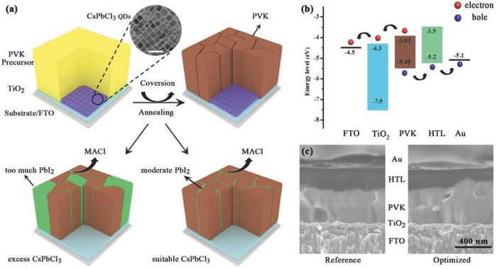
a) The conversion process for different CsPbCl3 contents. The inset is the TEM image of CsPbCl3 QDs, and the scale bar is 50 nm. b) Energy level diagram. c) The cross‐sectional SEM images of the devices based on the reference and CsPbCl3 optimized PVK film.
It should be noted that when a suitable amount of CsPbCl3 QDs is used to form just a surface layer of PbI2, the optimum passivation effect is observed. Any superfluous CsPbCl3 QDs will generate too much residual PbI2, thus inhibiting the charge transfer and collection.44 The energy level diagram of the PSCs is shown in Figure 1b, and the photogenerated carrier transport is illustrated as well.45, 46 The comparison of the cross‐sectional scanning electron microscopy (SEM) images (Figure 1c) of the devices with and without the CsPbCl3 QDs treatment indicates that the CsPbCl3 QDs have no obvious effect on the PVK grain growth beyond the surface passivation.
SEM, atomic force microscope (AFM), and energy‐dispersive X‐ray (EDX) are utilized to further investigate the composition and morphological evolution of the PVK films treated with different amounts of CsPbCl3 (0, 5, 20, and 50 mg mL−1). The SEM images of the representative PVK films are exhibited in Figure 2 a–d. All the obtained films display compact and uniform morphology without observable pinholes. Note that in the SEM images, components with different conductivities are displayed in different shades of gray.47, 48 The control film made without the CsPbCl3 QDs shows essentially all dark grains throughout the image, indicating only PVK grains without PbI2. When the CsPbCl3 QDs were introduced, white edges appeared around the PVK grain boundaries, indicating formation the PbI2 surface layers. The more CsPbCl3 QDs is used, the more PbI2 is observed. The white PbI2 phase covers almost half of the film when the CsPbCl3 concentration is increased to 50 mg mL−1. It is clear that the formation of PbI2 originated from the reaction of CsPbCl3 QDs with the PVK grain surfaces. Meanwhile, a similar phenomenon is also observed in the MAPbI3 film, as shown in Figures S1 and S2 and Table S1 in the Supporting Information.
Figure 2.
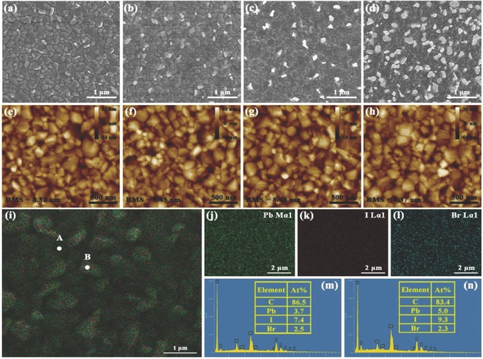
a–d) The SEM images and e–h) AFM images of PVK thin films (FA0.85MA0.15PbI2.55 Br0.45) formed using different amounts (0, 5, 20, and 50 mg mL−1, respectively) of CsPbCl3. i–l) The EDX elemental mappings and m,n) EDX spectra of PVK film using 50 mg mL−1 CsPbCl3 QDs at different locations.
However, the roughness and morphology of the films in the AFM images (Figure 2e–h) do not change with the addition of the various amounts of CsPbCl3. Such findings suggest that the CsPbCl3 only influences the component formation and has almost no effect on the morphology of the PVK thin film. The elemental mapping images and EDX analysis results are given in Figure 2i–n and confirm that the PVK films are composed of C, Pb, I, and Br but do not contain Cl. Figure 2m,n are, respectively, the EDX spectra of the dark (point A) and white (point B) grains in Figure 2i. The results demonstrate that residual PbI2 existed in the white grains, corresponding to the above SEM findings.
To further clarify the main role of CsPbCl3 in the formation of the PVK film, SEM images (Figure S3, Supporting Information) were acquired to observe the CsPbCl3 film before and after solvent treatment, which prove the CsPbCl3 film mainly adhered to the TiO2 film after PVK precursor treatment. Figure 3 a shows the X‐ray photoelectron spectroscopy (XPS) results of a TiO2 film deposited on FTO substrate (black line) and a CsPbCl3 QDs film treated with ethyl acetate (EA) and DMSO/GBL mixed solvent (3:7 v/v) on TiO2/FTO substrate. Obviously, O, Ti, and C are observed in both samples. In addition, the Cs 3d peaks, Pb 4f peaks, and Cl 2p peaks appear in the XPS spectrum of the CsPbCl3 QDs/TiO2/ FTO sample, which verifies the presence of CsPbCl3.
Figure 3.
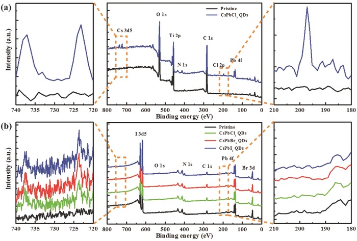
a) The XPS spectra of TiO2/FTO and CsPbCl3 QDs/TiO2/FTO film. b) The XPS spectra of pristine PVK thin films (FA0.85MA0.15PbI2.55 Br0.45) and films formed using 50 mg mL−1 of different components (CsPbCl3, CsPbBr3, and CsPbI3).
To understand the effect of Cl− on the PVK films, XPS measurements were performed for CsPbX3‐driven (X = Cl, Br, I) PVK films. Compared with the pristine reference, the 3d peaks of Cs still exist for all the samples, whereas the 2p peaks of Cl disappear. Consistent with the speculation and findings of Figure 2, these results indirectly demonstrate the formation of volatile MACl. To further clarify whether Cs and Pb or Cl in the QDs play an important role in the passivation of PVK films, the performance of CsPbX3 (X = Cl, Br, I) QDs‐driven PVK‐based PSCs are illustrated and compared in Figures S4 and S5 and Table S2 in the Supporting Information. It is clear that CsPbBr3 and CsPbI3 have almost no effect on the evolution of the morphology of the PVK films. Also, they have negligible or negative impact on the device performance, suggesting Cl− is critical for passivating the PVK films.
In order to study the effect of the CsPbCl3 QDs concentration on the structural and optical properties of PVK films, four representative samples with different contents of CsPbCl3 (0, 5, 20, and 50 mg mL−1) were selected as the research objects. To maintain identical test conditions, all the samples were prepared with the structure PVK/CsPbCl3/TiO2/FTO. The X‐ray diffraction (XRD) patterns (Figure 4 a) clearly confirm that the amount of PbI2 phase increases with increasing CsPbCl3, with is ascribed to the sublimation of MACl. These XRD results are coincident with those of the corresponding SEM images in Figure 2. The elemental proportions of Cs, Pb, Br, and I from the XPS measurements (Figure 4b) also indicate increasing PbI2 with increasing CsPbCl3, which is in agreement with the results of XRD and SEM.
Figure 4.
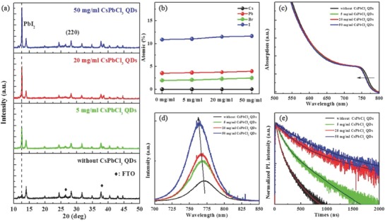
The structure and optical properties of PVK thin films (FA0.85MA0.15PbI2.55 Br0.45) formed using different amounts of CsPbCl3 (0, 5, 20, and 50 mg mL−1): a) XRD patterns, b) XPS elemental spectra, c) absorption spectra, d) PL spectra, and e) TRPL decay curves.
Figure 4c,d provides the absorption and photoluminescence (PL) spectra, respectively, of the pristine PVK films and those formed using different amounts of CsPbCl3. The observable bandgap widening and PL blueshift with increasing CsPbCl3 content mainly result from the existence of the PbI2 phase.44 It has been reported that the PbI2 could passivate the surface and grain boundaries of the PVK layer;49, 50 therefore, the PL intensity was remarkably increased with increasing CsPbCl3 content. Figure 4e compares the time‐resolved photoluminescence (TRPL) decay curves of the representative samples. The TRPL decay curves were fitted using a biexponential decay function [times (τi) and amplitudes (A i)], with the relevant key parameters listed in Table S3 in the Supporting Information. The average recombination lifetime (τave) was estimated using51, 52, 53
| (1) |
The lifetime is significantly prolonged from 0.13 to 1.24 µs with the increase of CsPbCl3 content, confirming that the PbI2 indeed passivates the defects in the grain boundaries in PVK films. The defects are considered recombination centers,54 and a longer lifetime is beneficial for extracting the photogenerated carriers.
Finally, the performances of different devices are compared to investigate the beneficial role of CsPbCl3 in the PSCs. Figure 5 a depicts the current density–voltage (J–V) curves of the devices fabricated without and with different CsPbCl3 contents. As the reference, the pristine device shows a PCE of 18.86%, with open‐circuit voltage (V OC), short‐circuit current density (J SC), and fill factor (FF) of 1.082 V, 22.87 mA cm−2, and 76.2%, respectively. With the introduction of the CsPbCl3, the device performance improved gradually with increasing QDs concentration. Even with the use of a small amount of CsPbCl3 QDs (5 mg mL−1), the device performance is improved significantly to a PCE of 19.35%, with the corresponding V OC, J SC, and FF improved to 1.101 V, 23.11 mA cm−2, and 76.1% respectively. When the CsPbCl3 content reached 20 mg mL−1, the PCE jumped to 20.09%. It is worth noting that both the J SC and V OC increased substantially. Given the prolonged lifetime, it is reasonable to attribute the improvement of the device performance to passivation of the traps by PbI2. However, further increasing the amount of CsPbCl3 QDs until there are too many CsPbCl3 QDs is not favorable to device performance, which is due to the wide bandgap (2.3 eV) of the resulting excess PbI2.55 The detailed parameters from the J–V curves are summarized in Table 2.
Figure 5.
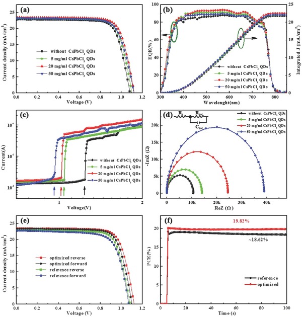
a) J–V curves. b) EQE spectra and integrated J sc. c) Dark I–V responses in capacitor‐like devices. d) Nyquist plots, with the inset presenting the equivalent circuit. e) J–V curves from both reverse scans and forward scans. f) PCE stability.
Table 2.
Static figures of merit for the reference and CsPbCl3 QDs optimized devices
| Device | Scanning mode | J SC [mAcm−2] | V OC [V] | FF [%] | PCE [%] | Hysteresis index |
|---|---|---|---|---|---|---|
| Reference | reverse | 22.87 | 1.082 | 76.2 | 18.86 | 0.055 |
| forward | 22.76 | 1.071 | 73.1 | 17.83 | ||
| Optimized | reverse | 22.45 | 1.122 | 76.4 | 20.09 | 0.027 |
| forward | 22.34 | 1.100 | 76.2 | 19.55 |
The typical external quantum efficiency (EQE) spectra of the devices are shown in Figure 5b. In the visible region, the EQE is highest for the device formed using 20 mg mL−1 CsPbCl3 QDs. The results further indicate that the CsPbCl3 QDs can enhance the device performance. It should be noted that the J SC values calculated using the EQE curves are consistent with those from the J–V measurements (errors less than 5%), indicating that the latter is well calibrated. The trap state densities (n t) in all the representative devices were estimated from the dark current–voltage (I–V) curves (Figure 5c). The applied voltage at the kink point, where the current increases and becomes nonlinear, is defined as the trap‐filled limit voltage (V TFL), which is determined by the defect density. The following equation relates V TFL to n t 56
| (2) |
where e is the elementary charge, L is the film thickness, ε is the relative dielectric constant, and ε0 is the vacuum permittivity. The calculated values of n t are shown in Table 1 for devices based on the pristine PVK films and those based on PVK films formed using different CsPbCl3 QDs contents. Distinctly, the trap state density decreases with increasing CsPbCl3 QDs amount. The reduced trap state density demonstrates the considerable improvement of the PVK film quality, resulting in the enhancement of the device performance. In parallel, the reduced trap state density is consistent with the prolonged lifetime in Figure 4e.
Table 1.
| CsPbCl3 [mg mL−1] | J SC [mAcm−2] | V OC [V] | FF [%] | PCE [%] | J SC(EQE) [mAcm−2] | τave [µs] | VTFL [V] | n t [cm−3] | τn [µs] |
|---|---|---|---|---|---|---|---|---|---|
| 0 | 22.87 | 1.082 | 76.2 | 18.86 | 21.76 | 0.13 | 1.24 | 1.37 × 10¹⁷ | 45.3 |
| 5 | 23.11 | 1.101 | 76.1 | 19.35 | 22.11 | 0.31 | 1.05 | 1.16 × 10¹⁷ | 71.2 |
| 20 | 23.45 | 1.122 | 76.4 | 20.09 | 22.55 | 1.07 | 1.02 | 1.13 × 10¹⁷ | 140.2 |
| 50 | 23.27 | 1.121 | 76.6 | 19.46 | 22.13 | 1.24 | 0.97 | 1.07 × 10¹⁷ | 276.5 |
To further elucidate the role of CsPbCl3 on the improved performance of PSCs, the carrier transport process and recombination behaviors are investigated by electronic impedance spectroscopy (EIS).57, 58 The Nyquist plots for the devices without and with different CsPbCl3 concentrations measured in the dark are shown in Figure 5d. The equivalent circuit model comprised of the series resistance (R s), the recombination resistance (R rec), and capacitance (C rec) is depicted in the inset of Figure 5d. In the high‐frequency region, the X‐axis intercept is the equivalent R s. The main arc is associated with the recombination process. The EIS parameters from the Nyquist plots are summarized in Table S4 in the Supporting Information. Clearly, the value of R s is decreased from 11.2 to 9.6 Ω after the CsPbCl3 modification. The reduced R s indicates that the introduction of the CsPbCl3 QDs facilitates the carrier transport. However, when the concentration of CsPbCl3 QDs is 50 mg mL−1, the R s is increased to 11.7 Ω, which is due to the excess PbI2 induced by the CsPbCl3. For R rec, the increasing values with increasing amount of CsPbCl3 mean that the carrier recombination is reduced. Given the identical conditions for all the PSCs, the increased R rec could be mainly ascribed to the microstructure evolution resulting from the effect of the CsPbCl3 addition. Meanwhile, from the complex plane curves, the effective lifetimes (τn) were extracted as the reciprocals of the frequencies corresponding to the peaks of the semicircles in the Cole–Cole plots.59 The τn for the optimized device (140.2 µs) is considerably longer than that of the pure PVK (45.3 µs), indicating that photogenerated carriers have more time to transport to the anode before possible recombination.
Hysteretic is a notorious behavior for planar PSCs. Figure 5e shows typical J–V curves of the devices measured using both reverse and forward scan directions, with key device parameters listed in Table 2 . It should be noted that J–V hysteresis was substantially eliminated by the addition of CsPbCl3, while the reference cell showed obvious hysteresis. The hysteresis index of the devices was defined by60
| (3) |
Clearly, the hysteresis index for the optimized device is 0.027, lower than 0.055 for the reference formed without CsPbCl3 addition.
To ensure the J–V measurement is reliable, the PCEs of the devices were recorded as a function of time with the cells biased at their respective V MP (voltage at the maximum power point, in this case 0.88 V for the reference and 0.90 V for the optimized device), as shown in Figure 5f. Clearly, the optimized device shows stable performance, while for the reference one, it exists some fluctuations which should be caused by the process of filling the uncertainty traps among grain boundaries under illumination. In general, both the stabilized PCE values are very close to those obtained by the direct J–V measurements. To confirm the process reproducibility, 50 individual devices (each) were fabricated from the reference and optimized films using the same procedure, with the statistical distribution of the key J–V parameters (V OC, J SC, FF, and PCE) presented in Figure S6 in the Supporting Information. All the key parameters exhibited fairly narrow distributions, indicating that the process was reproducible.
In summary, we adopted a thin CsPbCl3 QDs film to finely control the PbI2 content in planar PSCs, and we found that moderate residual PbI2 could result in stable and high‐efficiency solar cells. By fine‐tuning the residual PbI2 in the PVK layer accordingly, we have achieved a stable and high PCE of 20.09% with reduced hysteresis. We believe that more efficient and stable planar PSCs can be obtained in the future by employing interface engineering, crystal‐growth engineering, optical engineering, and compositional engineering.
Conflict of Interest
The authors declare no conflict of interest.
Supporting information
Supplementary
Acknowledgements
J.J., Z.J., and Q.W. performed the experiments, data analysis, and experimental planning. The project was conceived, planned, and supervised by Z.J., Q.W., and S.L. The manuscript was written by Q.W., Z.J., and S.L. All authors reviewed the manuscript. This work was funded by the National Key Research and Development Program of China MOST (2017YFA0204800/2016YFA0202400), the National Natural Science Foundation of China (61704099/61674098/91733301), Fundamental Research Funds for the Central Universities (GK201703026/GK201603054), the Natural Science Basic Research Plan in Shaanxi Province of China (Program No. 2017JQ2038), the Shaanxi Province Postdoctoral Science Foundation (2017BSHYDZZ04), and the Chinese National 1000 Talents Plan program (1110010341).
Jiang J., Jin Z., Gao F., Sun J., Wang Q., Liu S., Adv. Sci. 2018, 5, 1800474 10.1002/advs.201800474
Contributor Information
Zhiwen Jin, Email: jinzhiwen@snnu.edu.cn.
Qian Wang, Email: wangqian16@snnu.edu.cn.
Shengzhong (Frank) Liu, Email: szliu@dicp.ac.cn.
References
- 1. Dong Q., Fang Y., Shao Y., Mulligan P., Qiu J., Cao L., Huang J., Science 2015, 347, 967. [DOI] [PubMed] [Google Scholar]
- 2. Liu Y., Yang Z., Cui D., Ren X., Sun J., Liu X., Zhang J., Wei Q., Fan H., Yu F., Zhang X., Zhao C., Liu S. F., Adv. Mater. 2015, 27, 5176. [DOI] [PubMed] [Google Scholar]
- 3. D'Innocenzo V., Grancini G., Alcocer M. J. P., Kandada A. R. S., Stranks S. D., Lee M. M., Lanzani G., Snaith H. J., Petrozza A., Nat. Commun. 2014, 5, 3586. [DOI] [PubMed] [Google Scholar]
- 4. Miyata A., Mitioglu A., Plochocka P., Portugall O., Wang J. T.‐W., Stranks S. D., Snaith H. J., Nicholas R. J., Nat. Phys. 2015, 11, 582. [Google Scholar]
- 5. Zi W., Jin Z., Liu S. F., Xu B., J. Energy Chem. 2018, 10.1016/j.jechem.2018.01.027. [DOI] [Google Scholar]
- 6. Lin Y., Bai Y., Fang Y., Chen Z., Yang S., Zheng X., Tang S., Liu Y., Zhao J., Huang J., J. Phys. Chem. Lett. 2018, 9, 654. [DOI] [PubMed] [Google Scholar]
- 7. Jin Z., Yan J., Huang X., Xu W., Yang S., Zhu D., Wang J., Nano Energy 2017, 40, 376. [Google Scholar]
- 8. Bi D., Yi C., Luo J., Décoppet J.‐D., Zhang F., Zakeeruddin S. M., Li X., Hagfeldt A., Grätzel M., Nat. Energy 2016, 1, 16142. [Google Scholar]
- 9. Shin S. S., Yeom E. J., Yang W. S., Hur S., Kim M. G., Im J., Seo J., Noh J. H., Seok S. I., Science 2017, 356, 167. [DOI] [PubMed] [Google Scholar]
- 10. Feng J., Yang Z., Yang D., Ren X., Zhu X., Jin Z., Zi W., Wei Q., Liu F. S., Nano Energy 2017, 36, 1. [Google Scholar]
- 11. Wang Q., Dong Q., Li T., Gruverman A., Huang J., Adv. Mater. 2016, 28, 6734. [DOI] [PubMed] [Google Scholar]
- 12. Yang W. S., Park B. W., Jung E. H., Jeon N. J., Kim Y. C., Lee D. U., Shin S. S., Seo J., Kim E. K., Noh J. H., Science 2017, 356, 1376. [DOI] [PubMed] [Google Scholar]
- 13. Wu Y., Yang X., Chen W., Yue Y., Cai M., Xie F., Bi E., Islam A., Han L., Nat. Energy 2016, 1, 16148. [Google Scholar]
- 14. Wang Z., Lin Q., Chmiel F. P., Sakai N., Herz L. M., Snaith H. J., Nat. Energy 2017, 6, 17135. [Google Scholar]
- 15. Zhou N., Shen Y., Zhang Y., Xu Z., Zheng G., Li L., Chen Q., Zhou H., Small 2017, 13, 1700484. [DOI] [PubMed] [Google Scholar]
- 16. Bai Y., Meng X., Yang S., Adv. Energy Mater. 2017, 8, 1701883. [Google Scholar]
- 17. Fakharuddin A., Schmidt‐Mende L., Garcia‐Belmonte G., Jose R., Mora‐Sero I., Adv. Energy Mater. 2017, 7, 1700623. [Google Scholar]
- 18. Arora N., Dar M. I., Hinderhofer A., Pellet N., Schreiber F., Zakeeruddin S. M., Grätzel M., Science 2017, 358, 768. [DOI] [PubMed] [Google Scholar]
- 19. Chen Z., Dong Q., Liu Y., Bao C., Fang Y., Lin Y., Tang S., Wang Q., Xiao X., Bai Y., Deng Y., Huang J., Nat. Commun. 2017, 8, 1890. [DOI] [PMC free article] [PubMed] [Google Scholar]
- 20. Jiang J., Jin Z., Lei J., Wang Q., Zhang X., Zhang J., Gao F., Liu F. S., J. Mater. Chem. A 2017, 5, 9514. [Google Scholar]
- 21. Si H., Liao Q., Kang Z., Ou Y., Meng J., Liu Y., Zhang Z., Zhang Y., Adv. Funct. Mater. 2017, 27, 1701804. [Google Scholar]
- 22. Mao P., Zhou Q., Jin Z., Li H., Wang J., ACS Appl. Mater. Interfaces 2016, 8, 23837. [DOI] [PubMed] [Google Scholar]
- 23. Wei J., Li H., Zhao Y., Zhou W., Fu R., Leprince‐Wang Y., Yu D., Zhao Q., Nano Energy 2016, 26, 139. [Google Scholar]
- 24. Wang Q., Zhang X., Jin Z., Zhang J., Gao Z., Li Y., Liu F. S., ACS Energy Lett. 2017, 2, 1479. [Google Scholar]
- 25. Que M., Que W., Yin X., Chen P., Yang Y., Hu J., Yu B., Du Y., Nanoscale 2016, 8, 14432. [DOI] [PubMed] [Google Scholar]
- 26. Bella F., Griffini G., Correa‐Baena J. P., Saracco G., Grätzel M., Hagfeldt A., Turri S., Gerbaldi C., Science 2016, 354, 203. [DOI] [PubMed] [Google Scholar]
- 27. Zhang P., Wu J., Zhang T., Wang Y., Liu D., Chen H., Ji L., Liu C., Ahmad W., Chen Z. D., Li S., Adv. Mater. 2017, 30, 1703737. [DOI] [PubMed] [Google Scholar]
- 28. Saliba M., Matsui T., Domanski K., Seo J. Y., Ummadisingu A., Zakeeruddin S. M., Correabaena J. P., Tress W. R., Abate A., Hagfeldt A., Science 2016, 354, 206. [DOI] [PubMed] [Google Scholar]
- 29. Zhang H., Wang H., Williams S. T., Xiong D., Zhang W., Chueh C. C., Chen W., Jen A. K., Adv. Mater. 2017, 29, 1606608. [DOI] [PubMed] [Google Scholar]
- 30. Bai Y., Xiao S., Hu C., Zhang T., Meng X., Lin H., Yang Y., Yang S., Adv. Energy Mater. 2017, 7, 1701038. [Google Scholar]
- 31. Hadadian M., Correa‐Baena J.‐P., Goharshadi E. K., Ummadisingu A., Seo J.‐Y., Luo J., Gholipour S., Zakeeruddin S. M., Saliba M., Abate A., Grätzel M., Hagfeldt A., Adv. Mater. 2016, 28, 8681. [DOI] [PubMed] [Google Scholar]
- 32. Service R. F., Science 2016, 351, 113.26744388 [Google Scholar]
- 33. Bian H., Bai D., Jin Z., Wang K., Liang L., Wang H., Zhang J., Wang Q., Liu S., Joule 2018, 00087, 10.1016/j.joule.2018.04.012. [DOI] [Google Scholar]
- 34. Lee D. S., Yun J. S., Kim J., Soufiani A. M., Chen S., Cho Y., Deng X., Seidel J., Lim S., Huang S., Ho‐Baillie A. W. Y., ACS Energy Lett. 2018, 3, 647. [Google Scholar]
- 35. Guo Y., Wang Q., Saidi W. A., J. Phys. Chem. C. 2017, 121, 1715. [Google Scholar]
- 36. Bi C., Wang Q., Shao Y., Yuan Y., Xiao Z., Huang J., Nat. Commun. 2015, 6, 7747. [DOI] [PMC free article] [PubMed] [Google Scholar]
- 37. Hu Y., Zhang Z., Mei A., Jiang Y., Hou X., Wang Q., Du K., Rong Y., Zhou Y., Xu G., Han H., Adv. Mater. 2018, 30, 1705786. [DOI] [PubMed] [Google Scholar]
- 38. Ji F., Pang S., Zhang L., Zong Y., Cui G., Padture N. P., Zhou Y., ACS Energy Lett. 2017, 2, 2727. [Google Scholar]
- 39. Ye S., Rao H., Zhao Z., Zhang L., Bao H., Sun W., Li Y., Gu F., Wang J., Liu Z., Bian Z., Huang C., J. Am. Ceram. Soc. 2017, 139, 7504. [DOI] [PubMed] [Google Scholar]
- 40. Xie F., Chen C., Wu Y., Li X., Cai M., Liu X., Yang X., Han L., Energy Environ. Sci. 2017, 10, 1942. [Google Scholar]
- 41. Han G., Koh T. M., Lim S. S., Goh T. W., Guo X., Leow S. W., Begum R., Sum T. C., Mathews N., Mhaisalkar S., ACS Appl. Mater. Interfaces 2017, 9, 21292. [DOI] [PubMed] [Google Scholar]
- 42. Jiang Q., Zhang L., Wang H., Yang X., Meng J., Liu H., Yin Z., Wu J., Zhang X., You J., Nat. Energy 2016, 2, 16177. [Google Scholar]
- 43. Petrus M. L., Schlipf J., Li C., Gujar T. P., Giesbrecht N., Müller‐Buschbaum P., Thelakkat M., Bein T., Hüttner S., Docampo P., Adv. Energy Mater. 2017, 7, 1700264. [Google Scholar]
- 44. Jiang Q., Chu Z., Wang P., Yang X., Liu H., Wang Y., Yin Z., Wu J., Zhang X., You J., Adv. Mater. 2017, 29, 1703852. [DOI] [PubMed] [Google Scholar]
- 45. Fu Q., Tang X., Huang B., Hu T., Tan L., Chen L., Chen Y., Adv. Sci. 2018, 10.1002/advs.201700387. [DOI] [PMC free article] [PubMed] [Google Scholar]
- 46. Jin Z., Zhou Q., Chen Y., Mao P., Li H., Liu H., Wang J., Li Y., Adv. Mater. 2016, 28, 3697. [DOI] [PubMed] [Google Scholar]
- 47. Jin Z., Wang J., Sci. Rep. 2014, 4, 5331. [DOI] [PMC free article] [PubMed] [Google Scholar]
- 48. Zhang X., Wang Q., Jin Z., Zhang J., Liu S., Nanoscale 2017, 9, 6278. [DOI] [PubMed] [Google Scholar]
- 49. Kim Y. C., Jeon N. J., Noh J. H., Yang W. S., Seo J., Yun J. S., Ho‐Baillie A., Huang S., Green M. A., Seidel J., Adv. Energy Mater. 2016, 6, 1502104. [Google Scholar]
- 50. Jacobsson T. J., Correa‐Baena J. P., Halvani A. E., Philippe B., Stranks S. D., Bouduban M. E., Tress W., Schenk K., Teuscher J., Moser J. E., J. Am. Chem. Soc. 2016, 138, 10331. [DOI] [PubMed] [Google Scholar]
- 51. Zhang J., Bai D., Jin Z., Bian H., Wang K., Sun J., Wang Q., Liu F. S., Adv. Energy Mater. 2018, 10.1002/aenm.201703246. [DOI] [Google Scholar]
- 52. Bai D., Zhang J., Jin Z., Bian H., Wang K., Wang H., Liang L., Wang Q., Liu S. F., ACS Energy Lett. 2018, 3, 970. [Google Scholar]
- 53. Wang Q., Jin Z., Chen D., Bai D., Bian H., Sun J., Zhu G., Wang G., Liu S., Adv. Energy Mater. 2018, 10.1002/aenm.201800007. [DOI] [Google Scholar]
- 54. Chen Q., Zhou H., Song T.‐B., Luo S., Hong Z., Duan H.‐S., Dou L., Liu Y., Yang Y., Nano Lett. 2014, 14, 4158. [DOI] [PubMed] [Google Scholar]
- 55. Ma W., Yang F., Wang Y., Chen J., Yuan L., Xie D., Zhao Y., Zhang Y., Peng J., J. Mater. Sci. 2017, 52, 9696. [Google Scholar]
- 56. Zhang X., Jin Z., Zhang J., Bai D., Bian H., Wang K., Sun J., Wang Q., Liu S. F., ACS Appl. Mater. Interfaces 2018, 10, 7145. [DOI] [PubMed] [Google Scholar]
- 57. Zhang X., Wang Q., Jin Z., Chen Y., Liu H., Wang J., Li Y., Liu S., Adv. Mater. Interfaces 2018, 5, 1701117. [Google Scholar]
- 58. Jin Z., Wang A., Zhou Q., Wang Y., Wang J., Sci. Rep. 2016, 6, 37106. [DOI] [PMC free article] [PubMed] [Google Scholar]
- 59. Jin Z., Yuan M., Li H., Yang H., Zhou Q., Liu H., Lan X., Liu M., Wang J., Edward S., Li H. Y., Adv. Funct. Mater. 2016, 26, 5284. [Google Scholar]
- 60. Jiang J., Wang Q., Jin Z., Zhang X., Lei J., Bin H., Zhang Z.‐G., Li Y., Liu S., Adv. Energy Mater. 2018, 8, 1701757. [Google Scholar]
Associated Data
This section collects any data citations, data availability statements, or supplementary materials included in this article.
Supplementary Materials
Supplementary