Abstract
There is a growing demand for the development of new types of implantable optoelectronics to support both basic neuroscience and optogenetic treatments for neurological disorders. Target specification requirements include multi-site optical stimulation, programmable radiance profile, safe operation, and miniaturization. It is also preferable to have a simple serial interface rather than large numbers of control lines. This paper demonstrates an optrode structure comprising of a standard complementary metal-oxide-semiconductor process with 18 optical stimulation drivers. Furthermore, diagnostic sensing circuitry is incorporated to determine the long-term functionality of the photonic elements. A digital control system is incorporated to allow independent multisite control and serial communication with external control units.
Keywords: Active optrode, neural stimulation, optogenetics, implantable, self-diagnostic
I. Introduction
The optogenetic technique holds a remarkable potential for the realization of advanced neuroprostheses. By genetically expressing light-sensitive proteins such as channelrhodopsin-2 (ChR2) in cell membranes, targeted neurons in the brain or other neural tissue can be controlled by light [1]. This neuromodulation technique can be applied to both the exploration of extensive brain networks and potentially to provide effective therapies for neurological disorders.
For optogenetic stimulation, precise, intense, light delivery is an essential requirement. Classically, ChR2 requires a blue (470 nm) optical irradiance of ~1 mW/mm2 [2], [3]. Other variants are now available with lower thresholds and different wavelengths [4]. However, it is still the case that light scatters strongly in neural tissue. As such, light must either be delivered locally through a light-guide or generated locally to the tissue [5]. Each case has advantages and disadvantages.
Light guides [6]–[8] can be highly biocompatible, and as passive structures, do not cause heating of the brain tissue. Micro-fabricated probes with multiple light guiding structures have been successfully demonstrated since 2011 [9]–[12]. However, it is challenging to achieve efficient optical coupling and multiplexing. Furthermore, it is challenging to emit light at right angles to the probe. Thus, emitted light tends to traverse cortical layers rather than transmit through specific layers.
In contrast, if probes have local emissive elements, then multiplexing can be achieved electronically. Furthermore, radiance from emitters is typically perpendicular to the probe and will thus traverse along rather than through cortical layers. The caveat is that the emitters need to be efficient to ensure there is no negative tissue heating. Additionally, the overall design is more complex. Currently, micro-scale lasers do not function efficiently in the blue-green region of the optical spectrum. As such, the primarily available emitter class is gallium nitride-based (mini or micro) Light Emitting Diodes (LED) [13]. The primary difference between mini and micro LEDs is that the former is commercially available in dimensions down to  and can readily be bonded onto probes. The latter can be custom fabricated to dimensions of 20
  . The former is suitable for broader area emission and the latter for higher resolutions.
In 2013, Cao et al. demonstrated a probe which could record and emit light [14] via a single mini ( 1000
1000  ) LED. In 2013, McAlinden et al. demonstrated an optrode fabricated directly from Gallium Nitride (GaN), allowing multiple micro LEDs to be integrated onto the surface [15]. In the same year, Kim et al. proposed a multifunctional neural probe with GaN LEDs [16]. More recently micro LEDs transferred onto diamond [17] and silicon substrates have been demonstrated [18]. Recently Biederman et al. [19] demonstrated a control system which could externally multiplex and control emission. We have also previously demonstrated control electronics for 2D arrays of high radiance light emitters [13], [20]. However, electronic control, integrated within a probe has not yet been demonstrated.
In contrast in the field of electronic probes, a number of highly integrated probes exist which can record from a large number of electrodes simultaneously. Shulyzki et al. [21] have demonstrated a chip, which can be combined with existing 8  8 Utah style probes and up to 256 external recording pads. More interestingly Lopez et al. [22], and Angotzi et al. [23] have both demonstrated probes fabricated from a CMOS base which incorporates 455 and 512 recording electrodes respectively. These architectures utilize the shaft area for active electronics, which allows for much larger scale integration. But, these are purely electronic, and cannot be used for optogenetic applications.
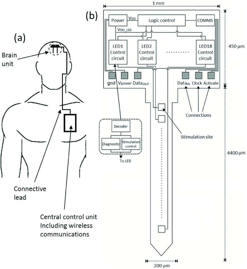
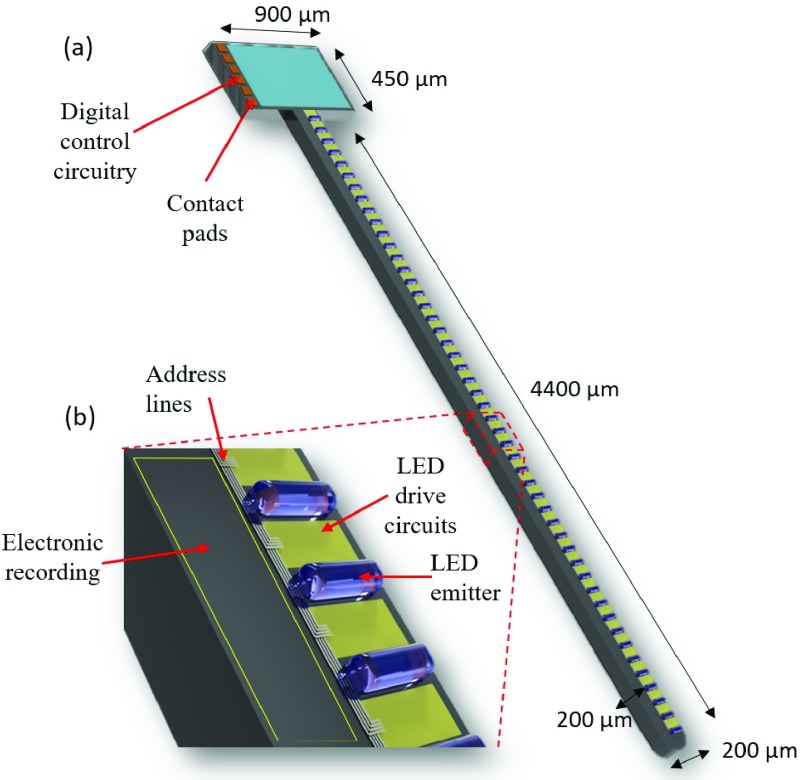
In this work, we propose to progress the concept of CMOS based active optoelectronic probes for the field of optogenetics. To our knowledge, this submitted work is the first scalable CMOS-based active optogenetic implant. It is possible to utilize the same post-fabrication techniques as for other probes to shape our probes and host sites for light emission and electrical recording. Our probes are designed to host GaN  LEDs. A conceptual diagram in Figure 1 demonstrates how this optrode would be utilized. A brain unit comprising of such probes would be controlled by an embedded control unit with digital communications between the two probes. Figure 1(a) demonstrates this for medical intervention. Figure 1(b) shows the key components we propose in this probe. We have previously [24], [25] demonstrated low-density optrode designs with consisting of
  LEDs. These were designed to use high efficiency mini-LEDs for brain pacemaking activity. In contrast, this paper seeks to explore probe architectures which can scale to a much higher density array, while still allowing for individual intensity and PWM control of individual LEDs. Depending on requirements, recording electronics as per Lopez et al. [22], and Angotzi et al. [23] could also be incorporated for closed-loop applications.
Fig. 1.
The system architecture of proposed optical probe. (a) A biomedical use of such a probe with a central control unit communicating over a digital communication method to the optrodes forming a brain implant. (b) The primary components of the optrode including communications, logic control and LED driver circuitry.
Moreover, since the optrode (including the LEDs) is intended to be implanted into brain tissue, the system stability is a key concern for long-term chronic operation. There is little data about how active probes would perform under such conditions. One hazard is that optrode may be damaged during or after implantation. Post-implantation, there may be corrosion of the individual light emitters. Since it would be challenging to evaluate the operation statuses of the optrode from external medical imaging, we have incorporated diagnostic sensing circuitry to assess the continued functional state of the optrode.
II. System Architecture
Our circuitry has been developed using a standard 0.35  CMOS process from X-FAB. The floorplan is shown in Figure 1(b). The optrode design consists of two primary parts: the optrode head in which all of the active circuitry is included, and the CMOS/silicon-based optrode shaft.
The length of the optrode shaft has been set to 4.4 mm, to match the thickness of primate brain cortical layers (which vary between 2 mm and 4.4 mm) [26]. As the cortex has up to six layers depending on the region, we have included six banks of individually controllable micro-photonic emitters, each with clusters of three micro-photonic emitters. Such clustering may make placement more convenient. The width of the shaft can be variable depending on LED size, but we assume a minimum  for structural rigidity.
Eighteen LED control modules have been generated in the optrode head to access the individual LED contact point. Each LED control module can perform both stimulation control function and diagnostic sensing function. Moreover, in order to address and control the whole system, a global communication and logic control module is implemented in the head part. This determines all of the input/output data of the optical stimulation circuitry and the diagnostic sensing circuitry. Subsequently, each LED point can be individually controlled and sensed. In addition, six I/O pads are implemented to either convey input/output signals or provide power supplies.
III. Control System
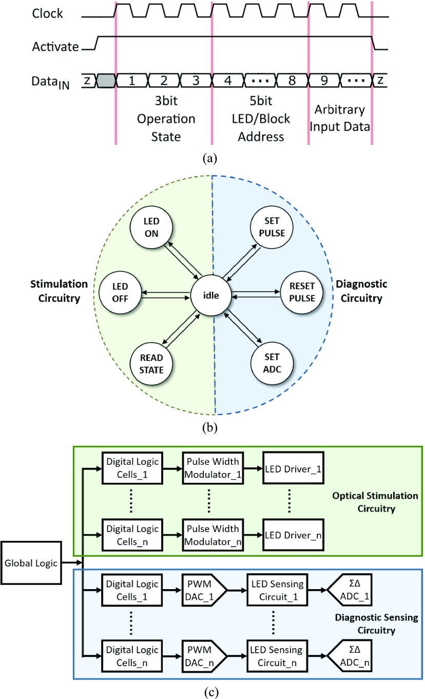
Figure 2 demonstrates the logic control subsystem. A modified serial peripheral interface (SPI) protocol has been developed for duplex communication, and the corresponding timing diagram is depicted in Figure 2(a). A global clock signal (Clock) is defined to synchronize all the logical operations of the optrode. An external activate (Activate) signal determines the state of a particular operation. A finite state machine (FSM) has been implemented to master all the operation states. All FSM states and corresponding transition conditions are illustrated in Figure 2(b). LED
 and LED
 are two major working patterns for the stimulation circuitry, and these two modes can manipulate the micro-photonic emitters with a predefined pulse width. The Read function is used to monitor the real-time status of the micro-photonic emitter via the pulse width modulator. Set_Pulse and Reset_Pulse are two input signals for the pulse modulated Digital-to-Analog Converter (DAC), which can achieve the voltage scanning scheme for diagnostic purposes. The Set_ADC is a trigger signal to enable or disable the Sigma-Delta Analog-to-Digital Converter (
 ADC). The
  ADC could then record the diagnostic sensing voltage, and the recorded data is then fetched via pulse expressions. Once the operation mode is decided, the targeted micro-photonic emitter would be consequently defined by LED addressing module. Then, the active micro-photonic emitter, LEDn, is selected by decoding the address information from input data Data
 . The flowchart of the overall system is displayed in Figure 2(c).
Fig. 2.
(a) Timing diagram of the modified SPI protocol. (b) Command trees of the FSM states and corresponding transition conditions. (c) Flowchart of the overall system, including logic control, optical stimulation circuitry, and diagnostic sensing circuitry.
IV. Optical Stimulation Circuitry
The neuron response will vary with the integral function of the irradiant density within short time periods [27], [28]. Thus, within a defined short period (frame) both pulse width modulation at a maximum amplitude or amplitude modulation are equally valid.
A. Light Requirement
There is a considerable body of work exploring the light requirement for optogenetic cells. The original 2003 paper [2] described the threshold as 0.7 mW/mm2. This threshold was confirmed for dissociated neural culture, e.g. by Han et al. [29]. Since then new types of opsins and in-vivo data have shown varying requirements, but the currently accepted value within the community is 1 mW/mm2 to achieve strong optical control.
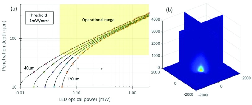
Wu et al. [18] and McAlinden et al. [15] have previously demonstrated modelling of light scattering behavior in neural tissue. In order to understand what this means in terms of the light emission, we have replicated this work for a LED emitting with a typical Lambertian (intensity varies with the cosine of the emission angle) profile. Results can be seen in Figure 3.
Fig. 3.
Light transmission in tissue (a) the optical power required for a Lambertian emitting LED to reach a certain penetration depth for a 1 mW/mm2 threshold. This is given for different emission region diameters from  to
to  . (b) the 3D profile of light penetration through tissue.
The light requirement depends on penetration depth as well as LED size. Plotting in this form, it is possible to determine the required absolute radiance (and thus required current) for a given LED diameter to reach a given penetration depth. We highlight the operational range given the circuit and LED efficiency parameters below.
To compare with previous literature, Wu et al. [18] developed non-electronic probes with built-in LEDs. They used LED currents of  to generate
  of optical power. They used modelling to estimate penetration depths of around
  at the 1 mW/mm2 target irradiance. This is more optimistic than our modelling shown in Figure 3. Nevertheless, they demonstrated the ability to stimulate nearby neurons. Another example is by McAlinden et al. [15] who utilized currents of up to 5 mA to generate radiances of 0.6 mW. The resultant penetration depth at the target irradiance was 175
  and matches our modelling in Figure 3.
The target range for this work is to achieve  at an irradiance of 1 mW/mm2. It should be noted that we expect to achieve greater depths in practice. For example, Wu et al. saw in-vivo responses at expected irradiances of 0.1 mW/mm2.
B. LED Characteristics
The design has been developed to utilize either custom fabricated  LEDs or mini-LEDs from commercial sources. In order to characterise the
  -
- and I-L (Luminance) relationships, we explored operation with both a
  diameter
  LED custom fabricated at the Tyndall Institute [30], [31], as well as a commercial surface mountable LNJ947W8CRA mini-LED from Panasonic (
 diameter).
I-V-L measurements were taken using the same approach described in the experimental section below, and a Verilog-A model was derived to inform our simulations. Based on the optical experiments, the  -
- -
- relationships of both
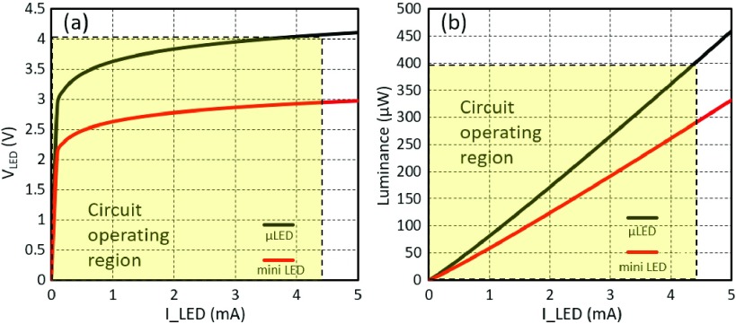
  LED and mini LED are illustrated in Figure 4. Moreover, we measured efficiencies for both LEDs at ~3%. The operating region of the circuit is shown in dotted lines. Although the global voltage
  is 5 V, 1 V is consumed by the
  of the drive transistor, thus limiting the output current, and therefore radiance.
Fig. 4.
I-V-L relationships of the  LED and the commercial Panasonic mini LED. The current through each LED is steadily increased from 0 mA to 5 mA. (a) I-V relationship. (b) I-L relationship. The efficiency measurement of both LEDs is around 3% which is consistent with the literature.
The measured efficiency was consistent with what has been provided in the literature to date for  LEDs in the optrode literature ([14], [15], [18]). In the long term, other groups developing mini and micro-LED architectures for other purposes have demonstrated have significantly better wall-plug efficiencies. For example, the CREE DA2432 mini LED [32] has efficiencies exceeding 30%. This is clearly a much larger LED (
 ), and thus not scalable to high integration. But Narukawa et al. [33] have demonstrated driving LEDs at similar current densities to micro-LEDs whilst still achieving 35% efficiency. As such, we believe that further progress to reduce series resistances and improve efficiency is possible in the micro-LED field.
An important final point to note is the heat emission from LEDs at the current and voltage levels above can cause heating of the probe. If only 3% of the input energy is converted to light, 97% is therefore converted to heat, limiting the ON time within for a given maximum surface temperature.
As the current, voltage and efficiency parameters are similar to that of McAlinden [15], we point to their study of the subsequent thermal effects on their passive probe (i.e. without circuitry). They estimate that the LED can be driven for up to 100 ms while seeing a maximum temperature rise of 1 °C over the 37 °C ambient.
C. LED Driver
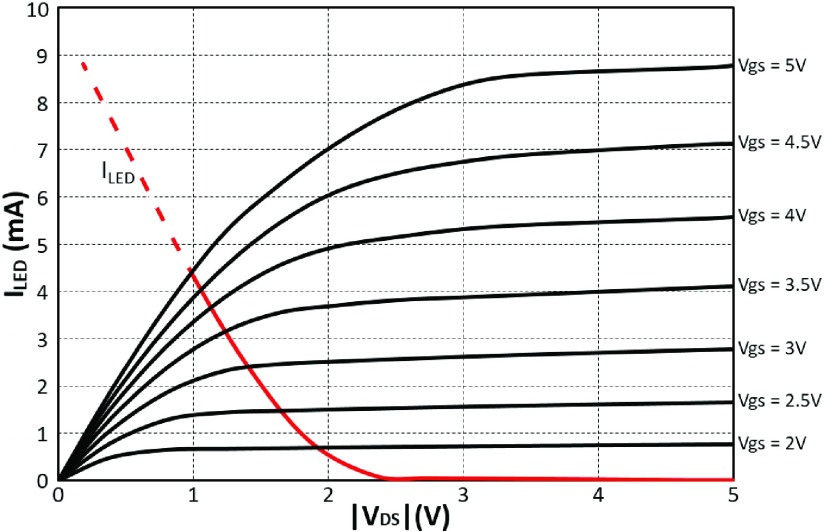
For blue LEDs, we expect an operational range between 3.5 and 4 V to achieve a target current of up to 4 mA. With a 1 V drop across the drive transistor, a 4 V operation is required. In the long term, if LED efficiencies are improved, the required current can come down. Additionally, if contact resistances are improved, the required voltage may be reduced to 4.5 V or perhaps slightly lower. If red LEDs are used in conjunction with red-shifted opsins, it would be theoretically feasible, assuming exceptional efficiencies, to bring the voltage down to within a 3.3 V domain. Thus, in this design, a 5 V pMOS transistor is utilized in the LED drive circuit. Given the trade-off between driving ability and dimensions, the  size of the pMOS drive transistor is set as
  . With a
  V, the maximum
  LED driving current is 4.4 mA. The maximum radiance is 400
  , which is sufficient for targeted local light delivery. Monte Carlo analysis was performed on the driver circuit indicating a standard deviation of
  or ~1%.
Figure 5 shows a load line plot for the drive transistor and the  LED. For much of the operation, the transistor will be in the triode region and thus acts more like a variable resistor than an ideal current source. This has a number of implications: to obtain ideal current driving in the saturation region would require a larger
  i.e.
i.e.  , thus:
  , where
  is voltage across the LED which is typically in the range 2.5 – 4 V depending on drive current. Such additional voltage would reduce the efficiency.
Fig. 5.
Load line plot for the drive transistor and the  LED. When
  V, the maximum value of
  is 4.4 mA, and corresponding utmost luminance is
  .
.
Operating the drive transistor in the triode region is more efficient as it minimizes the  drop across the drive transistor. However, the operational performance of LEDs bonded-on post fabrication will be more susceptible variability in contact resistances. As such, each LED would need to be individually calibrated post-fabrication.
The LEDs can be:
-
1)
ON supra-threshold – i.e. forward bias beyond 2.6 V with light emission. Our circuit is designed to drive this at a set voltage oscillated in time through pulse width modulation, and also the intensity.
-
2)
ON sub-threshold – i.e. forward bias below 2.6 V with no light emission. According to Cao et al. [34] and Xi et al. [35], the LED leakage operates in a thermally assisted hopping manner in the first ~1 V which is the same as the reverse leakage. As such, it is possible to determine the operational characteristics of the diode in the first few volts.
-
3)
OFF – i.e. in grounded state (and of course no light emission)
-
4)
REVERSE bias – not implemented on this design. But theoretically, there may be an advantage in biphasic operation – matching the positive phase with the negative phase from a degradation perspective [36]. However, it would also complicate the design as each LED would then need an individual cathode– reducing the potential integration density.
D. Pulse Width Modulator
The most efficient driving scheme for the LEDs in our design is pulse width modulation (PWM) at maximum intensity - assuming the droop profile of the LED (i.e. how the LED efficiency drops with increasing current) is low. This is because, with intensity modulation, efficiency decreases with decreasing light intensity because of the voltage drop across the drive transistor. For eight bits of intensity modulation within a typical frame time of 20 ms, the minimum required ON/OFF switching cycle is  .
.
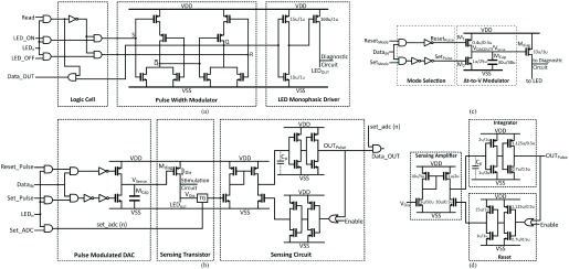
Each optical stimulation block has individual active logic circuitry to allow simultaneous operation of all LEDs. In order to pulse LED operation, the LED operation status (‘ON’ and ‘OFF’) needs to be maintained and updated in real time with particular stimulation cycles. The pulse width modulator keeps this working state constantly to maintain stimulation cycle until new data is pushed in and the new working mode is updated. A SR latch is used as a memory cell to maintain the ON state, as shown in Figure 6(a). In a post-layout simulation, the maximum frequency of the standalone SR cell is 125 MHz. Then this design is connected to the LED driver. The maximum switching frequency is recorded as 30 MHz which is significantly beyond the 50- minimum switching time requirement. The design was calculated to consume 63.9 fJ energy per cycle.
Fig. 6.
(a) Circuit schematic of stimulation control block.  signals determine the operation status of emitters. Read signal monitors the real-time working state saved by PWM unit. (b) A circuit schematic of diagnostic sensing block. Set_Pulse and Reset_Pulse generate pulse signals to achieve voltage scanning. Set_ADC determines the timing control of the
  ADC to fetch the
  . (TG is short for transmission gate). (c) Circuit schematic of the pulse width modulated DAC. This DAC performs two operations: mode selection and time-to-voltage conversion. (d) The diagnostic sensing element. Left is a (non-OTA) transconductance amplifier which feeds current into a simple
  ADC (right). This consists of three stages: current buffering, integration, and reset/pulse control.
V. Diagnostic Sensing Circuitry
A. Local Diagnostic Block
When the optrode is performing a normal light emission operation, the drive current through the LED will have a diode behavior with applied  until limited by the control transistor. There may, however, be an abnormality due to failure in the passivation, corrosion of LED contacts or even a critical failure such as probe fracture during insertion.
Electronically such scenarios may be seen as a resistance (corrosion in contacts or leak to tissue, or leak between the contacts). Should such processes continue, electrolytic degradation of the contact could lead to open circuit behavior (complete corrosion). An open circuit could also represent probe fracture. We believe these scenarios to be the primary route to degradation. There is an additional scenario whereby there is a rapid delamination of the encapsulation between the anode and cathode, e.g. this could happen between infrequent diagnostic sensing. This would look like a direct resistance between the anode and cathode– in parallel with the LED.
It is thus possible to analyze such effects (if they exist) by performing a DC voltage scan across a given LED and then determining the current-voltage profile. The local diagnostic sensing block consists of three different functioning modules (Figure 6(b)): a pulse-width modulated DAC, a source transistor  , and a sensing circuit. The latter consists of a low-gain transconductance amplifier and a one-bit
  ADC. The transistor sizing of the sensing block is given in Figure 6(d). The pulse-width modulated DAC (Described in
  ) determines the voltage
  and thus the
  on
on  . This transistor is operated in strong inversion triode mode as most of
  will drop across the LED.
In order to avoid turning on LED,  is varied between 4.25 and 3.5 V, i.e.
  - 1.5 V respectively. This is achieved by ensuring pulse widths are below 150 ns. Since the diagnostic function is expected to be operated without stimulating light emission, the
  is set as 10
  /1
/1  to limit the sensing current range into a safe region. The resulting sensing current (
 ) creates a voltage across
  in order to pass through the LED. As such, changes in the contact impedance at the anode or cathode will determine the profile of
  vs
vs  .
.
Ideally, the most accurate way to measure  is to utilise a full operational/instrumentation amplifier. However, the objective here is to explore scalable solutions whereby each LED has its own sensing circuit. As such the sensing circuit described in Figure 6(d) comprises of a low-gain transconductance amplifier (i.e. “sense amplifier”) connected to a
  ADC module (described in section
  ). The transconductance amplifier charges up a parasitic capacitor in the integrator stage, and the signal is then reset by the Reset stage. As the
  has an inverse relationship with a time interval (
 ) between an enable trigger and the output pulse, the
  can then be noted and reconstructed by recording the
  . The operational profile of this circuit is given in Table I.
TABLE I. Main Parameters of the Diagnostic Circuit.
| Technology | X-FAB 0.35- , 4M CMOS , 4M CMOS |
|---|---|
| Operation voltage | 3.3 V/5 V |
| Sampling points | 130/80 |
| Pulse modulated DAC | |
| Dynamic range | 43 dB/38 dB |
| Input voltage range | 0 - 3.3 V/5 V |
| Output voltage range | 0 - 3.3 V/5 V |
| Circuit area |  |
| Static power consumption | 3.7 fW/5.77 fW |
| Dynamic power consumption |  |
| Energy per sequence | (max) 10.3 pJ/24.3 pJ |
| Clock frequency | 10–100 MHz |
 ADC ADC | |
| Input voltage range | 0.75 - 3.3 V/0.75 - 5 V |
| Out pulse resolution | 10 ns |
| Dynamic range | 100 dB |
| Circuit area |  |
| Static power consumption | 1.6 fW/3.3 fW |
| Dynamic power consumption |  |
| Clock frequency | (max) 100 MHz |
Although the gain of the transconductance amplifier is low, providing between 4:444 nA for the range of 1:5 V, it is sufficient for most of the scenarios presented. However, it cannot sense  V i.e. when the amplifier stops being in strong inversion. As such, should the anode-cathode voltage drop below this (for example if in the short circuit case), then the output of the sensing amplifier will drop to zero. The output of the
  ADC will then timeout. If this is the case, although it cannot be characterised in detail, it gives a clear indication of failure.
Finally, a caveat to note with this circuit is that we would expect the post-processing variability to be greater than the CMOS variability. As such, we would expect that each LED in the probe would need to be tested and calibrated. But this can be part of the standard infant mortality tests for such devices.
B. Pulse Width Modulated DAC
This pulse width modulated DAC is based on an adapted switch-capacitor topology, as shown in Figure 6(c). This pulse modulated DAC requires only one digital input signal, and this signal contains the predefined pulse width information. The pulse signal is then combined with a mode selection signal (either Reset_Pulse or Set_Pulse) to determine the operation mode.
If enabling the reset mode, the  will be closed and
  will be kept open, and then a charge current would drop from
  to the capacitor. Consequently,
  will be charged up to
  . If the set mode is selected,
  will be in the open state, and
  is isolated from the capacitor. At the same time, the
  path will be clear, and
  will be gradually discharged until the Set_Pulse is terminated or
  is equal to
  . Using this strategy, the value of
  can be modulated from 0 V to
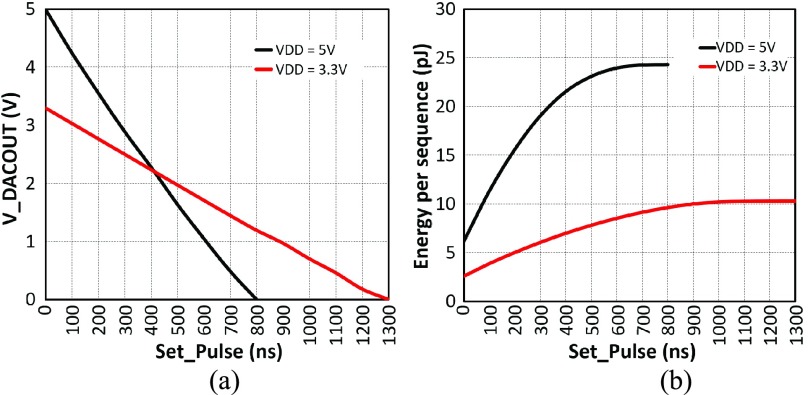
  (3.3 V or 5 V), corresponding to the input pulse width. The overall performance of the pulse modulated DAC is illustrated in Figure 7 and then summarized in Table I.
Fig. 7.
(a) Relationship between Set_Pulse and  . When
  is 5 V,
  is gradually decreased from 5 V to 0 V when Set_Pulse is swept from 0 ns to 800 ns. When
  is reduced to 3.3 V, the maximum value of Set_Pulse is increased to 1300 ns. (b) Energy consumption analysis per sequence.
  is set to 5 V and 3.3 V separately. The Reset_Pulse is still with the
  setting, and Set_Pulse signals are tuned in the 0 - 800 ns and 0 - 1300 ns ranges respectively. The maximum energy consumption per sequence is below 25 pJ. If needed, further reduction can be obtained by trimming the Reset_Pulse to 300 ns (the minimum charging time for
  ).
).
C. Sigma-Delta ADC
To accomplish the diagnostic circuitry, an ADC module is needed to fetch the diagnostic voltage  . Thus, this part presents a low-power miniature
  ADC, as shown in Figure 6(d). The
  ADC consists of two components: an integrator, and a reset. It receives current (4-444 nA) from the sensing amplifier which integrates over a parasitic capacitor
  (18 pF). Once the voltage on the capacitor reaches the threshold voltage on the first inverter stage of the integrator, the output of the
  ADC goes to
  . This feeds back to the reset circuit to discharge the parasitic capacitor, thus forming a pulse. An enable signal on the reset circuit allows for triggering the circuit, and hence either timing between the trigger and the output pulse or the pulse frequency within a given time.
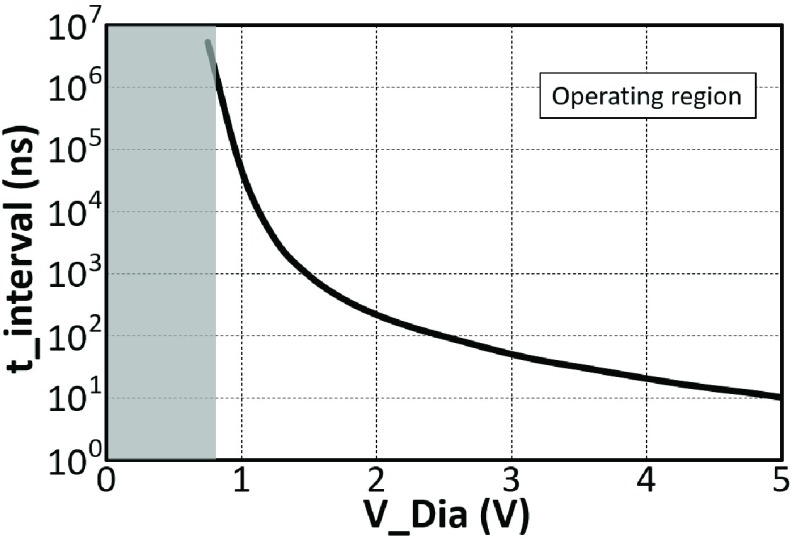
Given that small transistors were utilised in the integrator, a post-layout simulation was performed to certify its functionality. By tracing this simulation, the correlation between the input voltage and time interval ( ) were deduced subsequently, and the relationship is demonstrated in Figure 8. It can be seen that
  has a large dynamic range from 10 ns to more than
  ns (> 100 dB). However, as the operational region of the sensing amplifier is
  V, the operational dynamic range is
  i.e. 100 dB.
Fig. 8.
The relationship between time intervals of the output pulse versus the analog input voltage. The  has a large dynamic range from nanoseconds to milliseconds, which provides an outstanding sampling resolution.
Power analysis is also performed, and the average power consumption has been calculated. When this ADC operates with a 5 V power supply, the power consumption is 12.6  . When supply voltage decreases to 3.3 V, the power cost is then reduced to
  . Thus, this
  ADC demonstrates an appropriate power dissipation performance. Similar to the pulse modulated DAC, in actual use, the maximum operation frequency of this
  ADC is determined by the external controller (FPGA), i.e. 100 MHz in this work. Depending on the requirement, the operation frequency of the
  ADC can be much lower than 100 MHz. But to ensure appropriate resolution, 5 - 10 MHz clock frequency (dynamic range 70 - 80 dB) would be recommended. Table I summarizes the overall performance of the
  ADC.
ADC.
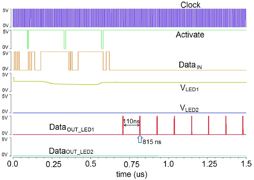
Then, the diagnostic sensing function is also fully validated via simulations, and Figure 9 illustrates the post-layout simulation results. It can be seen two LEDs (LED1 & LED2) are selected to conduct comparative analysis. LED1 is working in the diagnosis operation state, while LED2 maintains the off state consistently. The input Set_Pulse is defined as 150 ns to accomplish a 3.75 V  signal.
Fig. 9.
Top-level simulation results for the diagnostic sensing circuitry. A random LED  is chosen for analysis, and
  is selected for comparison. During this simulation,
  is set as 3.75 V (e.g. —
 — is equal to 1.25 V), the diagnostic voltage is equal to 2.40 V, and the
  is correspondingly equal to 110 ns. The local circuit schematic is referred to Figure 6(b).
During the simulation, the Clock signal defines the operation frequency, and the Activate signal controls the diagnostic sensing operation. All of the input information, which can be serially used to achieve system addressing, logic controlling, and pulse signals configuration, are transmitted via Data
 signal. In the output part, it can be observed that, after the PWM stage,
  (
( ) is equal to 2.40 V constantly. In contrast,
  still maintained at 0.0 V. The second pulse of the Data
 can be seen at 815 ns, giving a pulse interval of 110 ns. For comparison, no pulsing is seen in Data
 .
.
In this diagnostic sensing circuit, as mentioned above, the  signal is regulated by the pulse width of the Set_Pulse. Then, the accuracy of
  modulation relies on the resolution of the pulse width modulated DAC. Likewise, through the
  ADC, the subsequent
  voltage is expressed by a pulse frequency with the time interval
  .
.
VI. CMOS Implementation
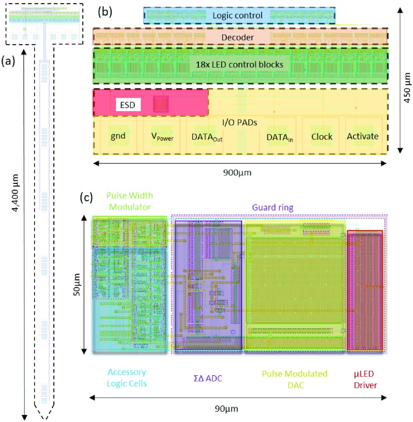
This optrode has been implemented and fabricated in a X-Fab 0.35- 4-metal multi-layer mask wafer process. The global layout and micrograph of the fabricated chip are displayed in Figure 10. The total chip outline on the reticle is
  4850
4850  , which fits with the proposed architecture in Figure 1. The dimensions of the global logic control block are
  , and the size of the 18 micro-photonic emitter control & sensing blocks is
  . The shaft length is 4400
  , in accordance with the six cortical layers. The micro-photonic emitter anode pad is 60
  . Additionally, the width of metal wirings and spacing is 40
  on each side. Six micro-photonic emitter clusters are evenly placed along the optrode shaft, and the spacing between each two micro-photonic emitter clusters is 580
  . This should potentially allow for a micro-photonic emitter cluster per cortical layer, though in practice there is a wide variation in cortical layer thicknesses depending on region [26]. In each micro-photonic emitter cluster, only a 20
  spacing is set between each two micro-photonic emitters. This ensures that those two backup micro-photonic emitters could have a very similar penetration area to that of the main micro-photonic emitter. In addition, the top metal layer metal-L is retained and utilized as a shield for light reflection protection and noise isolation.
Fig. 10.
(a) Layout diagram of the optrode. (b) The primary circuitry in the head: six I/O pads are used for power supply and digital & analog I/O, with custom-designed electrostatic discharge (ESD) protection circuitry. The 18 local control blocks consume  die area in total. The size of the 18-bit decoder is
  . (c) The layout of integrated local stimulation and diagnostic circuitry. A guard ring is utilized to insulate the analog and digital parts. The area of this local block is only 0.0035 mm2.
VII. Post-Fabrication
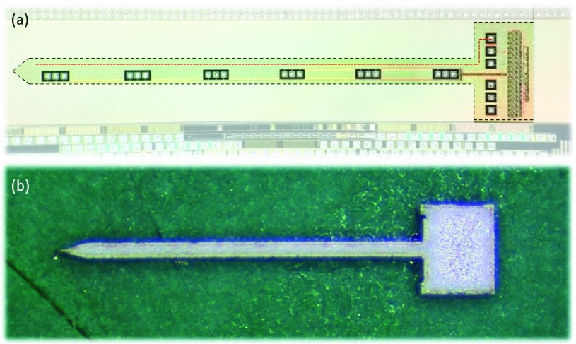
A physical layout can be seen in Figure 11(a). The exact cut-out dimensions can be determined according to the user need. Tips can be either blunt or sharp. Sharper tips reduce the required penetration force [37] but increase the potential insertion damage. At a width of  , the probe aspect ratio would be 22, which should be sufficiently low to prevent buckling on insertion.
Fig. 11.
(a) A photograph of the fabricated chip with the primary areas highlighted. (b) An optrode cut out of a (non-CMOS) silicon wafer using a laser ablation method.
This work focusses on the circuitry to implement a scalable active optogenetic probe. We, therefore, do not demonstrate full post-fabrication. However, this architecture is compatible with the efforts of Cao [14] and Wu [18]. i.e. a barrier layer, typically titanium or tungsten followed by gold needs to be deposited on the CMOS and LED anode/cathode contact pads. The LEDs need to then be placed on the CMOS optrode and bonded. We would envisage the LEDs being deposited as a single strip to simplify the process. The optrode would then need to be cut out using laser cutting (see Figure 11(b), or a reactive ion etching technique.
Figure 11(a) shows our CMOS device with the optrode dimensions. To demonstrate feasibility, Figure 11(b) shows an exemplar cut-out on normal silicon, using laser-based cutting. All experiments were performed on standard packaged die, as the clean room fabrication technique will be perfected and implemented later.
VIII. Measurement Results
A. Experiment Set-Up
The general testing set-up included a Keithley 2602B source meter is utilized to provide the 5 V  and the global
  . A Xilinx Virtex-7 FPGA board is selected to configure and control the testing chip package, to support the high-frequency operation of the pulse width modulated DAC. An Agilent 34460A multimeter is used to probe and sense particular analog signals (such as
  , and
, and  ), while time domain measurement is captured by an Agilent MSO-X 4034A oscilloscope.
Light measurement was achieved by placing a Newport UV-818 calibrated photodiode face-down on an optrode. Currents were then measured using a Keithley source measure unit, and converted to light intensity using the calibration chart provided by Newport. This is the standard method that has been utilized by others [14], [15], [18]. There is, however, a caveat with this approach. We noticed that slight angular torsion of the probe could lead to significantly lower results. Furthermore, even when we achieved optimal alignment, there was some reflection from the photodiode surface, indicating that not all the light was absorbed. As such, we feel our measurements are quite conservative.
B. Optical Stimulation Function
In this part, the optrode stimulation control function has been verified on the bench after setting up the test platform. The input signals (Clock, Activate and Data
 ) are all generated from the FPGA Virtex-7 board. The primary purpose of the test is to validate the light driving ability of the proposed optrode with the tunable power supply. A solitary
  LED is wire-connected between the LED anode pad and global
  , to measure the drive current. During the measurements,
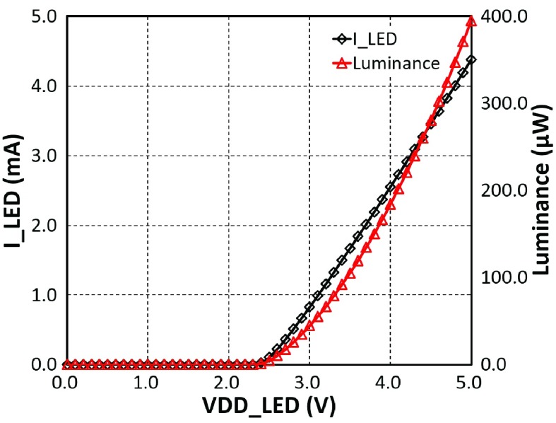
  is steadily adjusted from 0.0 V up to 5.0 V with 0.1 V steps. Measurement results are demonstrated in Figure 12. When
  is lower than the
  LED working threshold, the value of
  is at the fA or nA level. When
  is above the threshold, then the light emitter is activated to perform a linear relationship between
  and
and  . It can be seen that, when
  is equal to 5.0 V, the maximum working
  is 4.37 mA, and the corresponding effective luminance is 395
  . These results closely match the results shown in Figures 4, 5. This demonstrates that this optrode can generate sufficient luminance with high accuracy, and the targeted light delivery and penetration depth can be achieved.
Fig. 12.
On-bench measurement results for the  LED current and luminance versus
  . The local circuit schematic is referred to Figure 6(a).
C. Diagnostic Sensing Function
The functionality of the diagnostic sensing circuitry has been assessed using the same test platform described above. The sampling points are defined as  , 1, 1.25, and 1.5 V, respectively.
To verify the normal operation, a  LED was connected to the LED anode PAD and global
  . Next, possible degradation mechanisms can be represented as increased resistance or capacitive open circuit. Here, a 500
  resistor is picked to act as the increased resistance. It is then serially connected with the
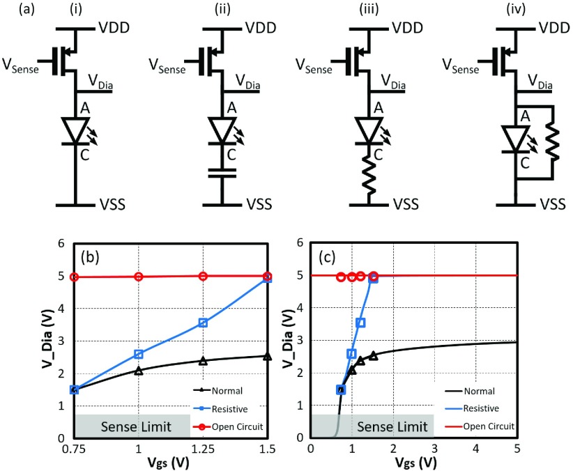
  LED to emulate the corrosion status (resistive state). Meanwhile, to mimic the open circuit, a 10 pF capacitor is connected to the LED PADs. As the resistance of the stimulation site is higher than expected, it can be reflected and extracted by the
  . The comparison measurement results of the four-state operations are shown in Figure 13. It can be seen from Figure 13(b) that the black curve represents the normal operation: When
  is in the predefined range, the normal
  varies from 1.5 V to 2.5 V. The blue curve demonstrates the corrosion state; with same sampling points, the resistive
  is increased from 1.5 V up to 5 V. The red line expresses the optrode rupture status; as an open circuit is formed, the
  is equal to 5 V constantly. These measurement results match with the simulation results in Figure 13(c). Therefore, given predefined sampling points, the implant working status can be observed in real-time, and breakage and/or corrosion points will be accordingly detected.
Fig. 13.
(a) Equivalent four-state circuit model. (b) Comparison measurement results of three-state  LED operation conditions. (c) Measurement results overlay with the simulation results. The equivalent circuit schematic is referred to Figure 6(b).
D. Power Consumption
Based on all the simulation and measurement results previously obtained, the system power consumption of this optrode is calculated and summarized in Table II. It can be seen that the total power consumption of the optrode is 1.008 mW when only one  LED is turned on at the same time. In particular, the light power consumes the majority of the system power (1.005 mW, 99.7%). In actual use, depending on the battery capacity, up to
  LEDs can be simultaneously turned on in the single optrode, or multiple optrodes can be manipulated at the same time if only one specific
  LED needs to be activated.
TABLE II. Total Power Consumption of The Proposed Optrode.
| Subsystem | Major Circuits | Static power ( ) ) |
Dynamic power ( ) ) |
Utilized circuits duty cycle | Total power ( ) ) |
|---|---|---|---|---|---|
| Logic control | FSM | 0.00 | 2 | 100% | 2 |
| Optical Stimulation | Pulse width modulator | 0.00 |  |
100% |  |
| Logic cells | 0.00 |  |
100% |  |
|
 LED LED |
 |
5% | 1005 | ||
| Diagnostic sensing | Pulse modulated DAC |  |
8.45 | 1% | 0.0845 |
| Sensing transistor | 100 | 1% | 1 | ||
 ADC ADC |
 |
12.6 | 1% | 0.126 | |
Total Power ( W) W) |
1008.21 | ||||
IX. Discussion and Conclusion
This paper has presented a CMOS-based optrode for optoelectronic/optogenetic neural stimulation. The overall system performance of the circuitry in tandem with  LEDs has been characterized and summarized in Table III.
TABLE III. Performance Summary of The Proposed Optrode and Comparison With Other CMOS Active Neural Probes.
| System Overview | ||||
|---|---|---|---|---|
| This work | [21] | [22] | [23] | |
| Year | 2017 | 2014 | 2014 | 2015 |
| Technology | 0.35- , 4-metal X-Fab CMOS process , 4-metal X-Fab CMOS process |
0.35- CMOS process CMOS process |
0.18- CMOS process CMOS process |
0.18- CMOS process CMOS process |
| Operation voltage | 5.0 V | 3.0 V | 1.8 V | 1.8 V |
| Die area | 1.36 mm2 | 12.77 mm2 | 10.57 mm2 | 4 mm2 |
| Probe head size |  |
- |  |
- |
| Probe shaft size |  |
- |  |
 |
| Site area |  |
0.02 mm2 (sti)/ 0.035 mm2(rec) |  |
 |
| No. stimulation sites | 18 (scalable to 88) (optical) | 64 (electrical) | N/A | N/A |
| No. recording sites | N/A | 256 | 52 (455 electrodes) | 16 (512 electrodes) |
| Total power | 1.01 mW ( LED)/ 6.04 mW ( LED)/ 6.04 mW ( LEDs) LEDs) |
13.5 mW | 1.45 mW | - |
| Optical Stimulation | ||||
No.  LEDs LEDs |
18 (scalable to 88) | N/A | N/A | N/A |
 LED current range LED current range |
0 - 4.37 mA | |||
| Maximum luminance |  |
|||
| Modulation methods | Pulse width modulation | |||
| Diagnostic Sensing | ||||
| No. sampling points (Min) | 4 | N/A | N/A | N/A |
| Sampling rate (Max) | 100 MHz | |||
| Input sensing current | 0 
|
|||
| Output diagnostic voltage | 0.75 - 5.0 V | |||
An important aspect of the circuitry we have developed is the scalability of the dimensions, as seen in Figure 10(c). If we consider the LED driver as a primary ‘pixel’ with a size of 90  , it could easily be patterned along the shaft, as per Figure 14. Assuming
  are required for the micro-photonic emitter bonding, then a repeat unit would be
  , allowing for 49 micro-photonic emitters along the optrode shaft. If circuit-under-pad techniques are used, then the repeat spacing could be 50
  , allowing for 88 micro-photonic emitters. Furthermore, scalability includes effectively independent pulse-width and intensity control on each pixel.
Fig. 14.
Scalable architecture of the proposed CMOS optrode. The overall size matches with the architecture in Figure 1. Using the outlined dimensions [width  , length
  , thickness
  ], 49 micro-photonic emitters could be integrated along the shaft. The area outlined in part (b) allows for integration of neural recording circuitry in the future.
Micro-photonic emitter dimensions vary in the literature. We have previously presented devices with total dimensions of 320  [32],
[32],  [30] and 80
  [13]. McAlinden et al. [15] demonstrated a LED with anode diameter of
  . Wu et al. [18] demonstrated
  . As such, we feel the proposed dimensions above to be conservative.
Finally, a self-diagnosis sensing scheme has been proposed to assess the optrode integrity and degradation in real-time. To note, this diagnostic circuit can work with both 3.3 V and 5 V voltages, but the LED requires 5 V for high radiance stimulation. Thus, we utilise a 5 V transistor for both stimulation circuit and diagnostic circuit, and mixed circuitry with 3.3 V for non LED-facing transistors will be explored in the future. Though simple, this self-diagnostic function allows for system diagnostics in vivo cases, where it is the only effective way of determining continued effective function of the probe. This would be beneficial for both circuit operation and tissue health.
Acknowledgment
The authors would also like to thank Prof. Nick Donaldson at UCL for performing exploratory laser fabrication in Figure 11.
Biographies

Hubin Zhao (S’12–M’16) received the Ph.D. degree in bio-electronics from Newcastle University, U.K., in 2016. He received the Best Paper Award from the IEEE conference on BioCAS 2014. He was the Chair of the IEEE Newcastle University Student Branch from 2014 to 2016 and is the mentor of the IEEE NCL SB from 2016 to 2017. He is currently a Post-Doctoral Research Associate and a Guest Lecturer with the University College London, U.K. He is also with the neoLAB, Cambridge University, U.K. His research interests mainly include brain–computer interface, implantable & wearable electronics, biomedical circuits and neural interface, and advanced opto-electronic technology.

Ahmed Soltan (M’14) received the B.Sc. and M.Sc. degrees from the University of Cairo, Cairo, Egypt, in 2004 and 2008, respectively, the Ph.D. degree in electronics and communication from Cairo University in 2014. He is currently a Research Associate with the School of Electrical Engineering, Newcastle University. His current research interest is about designing low power systems for implementable biomedical devices. He is also interested in the investigation of fractional circuits and systems, specifically in fractional order analog filters for signal processing and fractional order modeling for biomedical applications.

Pleun Maaskant received the M.Sc. degree in applied physics from the University of Groningen, Groningen, The Netherlands, in 1980. He has been the Principal Investigator in over 15 different projects funded by Enterprise Ireland, Science Foundation Ireland, and the European Space Agency. He is currently a Senior Staff Scientist with the Tyndall National Institute, University College Cork, Cork, Ireland, where he has been involved in research on gallium nitride-based devices for almost 20 years. He is the Inventor of the microLED, which has been patented and commercialized by the Irish SME InfiniLED.
Na Dong, photograph and biography not available at the time of publication.
Xiaohan Sun, photograph and biography not available at the time of publication.

Patrick Degenaar (SM’15) received the degree (Hons.) in applied physics and the M.Res. degree in surface science from Liverpool University, Liverpool, U.K., in 1996 and 1997, respectively, and the Ph.D. degree in bioelectronics from the Japan Advanced Institute of Science and Technology in 2001. He was a Post-Doctoral Researcher at the Imperial College, London, he received an RCUK Fellowship and was promoted to faculty in 2005. He was the coordinator of the FP7 OptoNeuro Project, which led to this research. He is currently the Workpackage Team Leader of the Flagship CANDO Project aiming to deliver a clinical optogenetic device for epilepsy. In 2010, he moved his team to Newcastle University, where he is currently a Reader in neuroprosthetic engineering with the Microsystems Group, School of Electrical and Electronic Engineering. In addition to his interests in retinal prosthesis, he has a significant interest in developing a clinical program for visual-cortical prosthesis.
Funding Statement
This work was supported in part by the European Commission OptoNeuro FP7 Program under Grant 249867 and the Wellcome Trust-EPSRC through the CANDO Project under Grant NS/A000026/1. The work of H. Zhao was supported in part by the Newcastle University Doctoral Scholarship and the GBCET-SC Scholarships.
References
- [1].Fenno L., Yizhar O., and Deisseroth K., “The development and application of optogenetics,” Annu. Rev. Neurosci., vol. 34, pp. 389–412, Jul. 2011. [DOI] [PMC free article] [PubMed] [Google Scholar]
- [2].Nagel G.et al. , “Channelrhodopsin-2, a directly light-gated cation-selective membrane channel,” Proc. Nat. Acad. Sci. USA, vol. 100, no. 24, pp. 13940–13945, 2003. [DOI] [PMC free article] [PubMed] [Google Scholar]
- [3].Barrett J. M., Berlinguer-Palmini R., and Degenaar P., “Optogenetic approaches to retinal prosthesis,” Vis. Neurosci., vol. 31, pp. 345–354, Sep. 2014. [DOI] [PMC free article] [PubMed] [Google Scholar]
- [4].Kurihara M. and Sudo Y., “Microbial rhodopsins: Wide distribution, rich diversity and great potential,” Biophys. Physicobiol., vol. 12, pp. 121–129, Dec. 2015. [DOI] [PMC free article] [PubMed] [Google Scholar]
- [5].Pisanello F., Sileo L., and De Vittorio M., “Micro- and nanotechnologies for optical neural interfaces,” Frontiers Neurosci., vol. 10, p. 70, Oct. 2016. [DOI] [PMC free article] [PubMed] [Google Scholar]
- [6].Tamura K.et al. , “A glass-coated tungsten microelectrode enclosing optical fibers for optogenetic exploration in primate deep brain structures,” J. Neurosci. Methods, vol. 211, no. 1, pp. 49–57, 2012. [DOI] [PubMed] [Google Scholar]
- [7].Wang J.et al. , “Integrated device for combined optical neuromodulation and electrical recording for chronic in vivo applications,” J. Neural Eng., vol. 9, no. 1, p. 016001, 2012. [DOI] [PubMed] [Google Scholar]
- [8].Abaya T. V. F., Blair S., Tathireddy P., Rieth L., and Solzbacher F., “A 3D glass optrode array for optical neural stimulation,” Biomed. Opt. Exp., vol. 3, no. 12, pp. 3087–3104, 2012. [DOI] [PMC free article] [PubMed] [Google Scholar]
- [9].Doroudchi M. M.et al. , “Towards optogenetic sensory replacement,” in Proc. Annu. Int. Conf. IEEE Eng. Med. Biol. Soc., Aug./Sep. 2011, pp. 3139–3141. [DOI] [PMC free article] [PubMed] [Google Scholar]
- [10].Kobayashi R.et al. , “Development of Si neural probe with optical waveguide for highly accurate optical stimulation of neuron,” in Proc. 5th Int. IEEE/EMBS Conf. Neural Eng., Apr./May 2011, pp. 294–297. [Google Scholar]
- [11].Dong N., Sun X., and Degenaar P., “Implantable optrode design for optogenetic visual cortical prosthesis,” Proc. SPIE, vol. 8207, pp. 82076A-1–82076A-10, Feb. 2012. [Google Scholar]
- [12].Paralikar K.et al. , “An implantable 5 mW/channel dual-wavelength optogenetic stimulator for therapeutic neuromodulation research,” in IEEE Int. Solid-State Circuits Conf. (ISSCC) Dig. Tech. Papers, Feb. 2010, pp. 238–239. [Google Scholar]
-
[13].Soltan A.et al. , “High density, high radiance
 LED matrix for optogenetic retinal prostheses and planar neural stimulation,” IEEE Trans. Biomed. Circuits Syst., vol. 11, no. 2, pp. 347–359, Apr.
2017. [DOI] [PubMed] [Google Scholar]
 -
[14].Cao H., Gu L., Mohanty S. K., and Chiao J. C., “An integrated
 LED optrode for optogenetic stimulation and electrical recording,” IEEE Trans. Biomed. Eng., vol. 60, no. 1, pp. 225–229, Jan.
2013. [DOI] [PubMed] [Google Scholar]
 - [15].McAlinden N.et al. , “Thermal and optical characterization of micro-LED probes for in vivo optogenetic neural stimulation,” Opt. Lett., vol. 38, no. 6, pp. 992–994, 2013. [DOI] [PubMed] [Google Scholar]
- [16].Kim T.-I.et al. , “Injectable, cellular-scale optoelectronics with applications for wireless optogenetics,” Science, vol. 340, pp. 211–216, Apr. 2013. [DOI] [PMC free article] [PubMed] [Google Scholar]
- [17].Boudet A., Scharf R., Dawson M., and Mathieson K., “A diamond-based, hybrid optrode for multisite optogenetics,” in Frontiers Opt. OSA Tech. Dig., New York, NY, USA, 2016, paper FTh4D.5. [Online]. Available: https://www.osapublishing.org/abstract.cfm?URI=FiO-2016-FTh4D.5 [Google Scholar]
-
[18].Wu F., Stark E., Ku P.-C., Wise K. D., Buzsáki G., and Yoon E., “Monolithically integrated
 LEDs on silicon neural probes for high-resolution optogenetic studies in behaving animals,” Neuron, vol. 88, no. 6, pp. 1136–1148, 2015. [DOI] [PMC free article] [PubMed] [Google Scholar]
 - [19].Biederman W.et al. , “A 4.78 mm 2 fully-integrated neuromodulation SoC combining 64 acquisition channels with digital compression and simultaneous dual stimulation,” IEEE J. Solid-State Circuits, vol. 50, no. 4, pp. 1038–1047, Apr. 2015. [Google Scholar]
- [20].Berlinguer-Palmini R.et al. , “Arrays of MicroLEDs and astrocytes: Biological amplifiers to optogenetically modulate neuronal networks reducing light requirement,” PLoS ONE, vol. 9, no. 9, p. e108689, 2014. [DOI] [PMC free article] [PubMed] [Google Scholar]
- [21].Shulyzki R.et al. , “320-channel active probe for high-resolution neuromonitoring and responsive neurostimulation,” IEEE Trans. Biomed. Circuits Syst., vol. 9, no. 1, pp. 34–49, Feb. 2015. [DOI] [PubMed] [Google Scholar]
- [22].Lopez C. M.et al. , “An Implantable 455-active-electrode 52-channel CMOS neural probe,” IEEE J. Solid-State Circuits, vol. 49, no. 1, pp. 248–261, Jan. 2014. [Google Scholar]
- [23].Angotzi G. N., Malerba M., Zucca S., and Berdondini L., “A 512-channels, whole array readout, CMOS implantable probe for acute recordings from the brain,” in Proc. 37th Annu. Int. Conf. IEEE Eng. Med. Biol. Soc. (EMBC), Aug. 2015, pp. 877–880. [DOI] [PubMed] [Google Scholar]
- [24].Zhao H.et al. , “A CMOS-based neural implantable optrode for optogenetic stimulation and electrical recording,” in Proc. IEEE Biomed. Circuits Syst. Conf. (BioCAS), Oct. 2015, pp. 1–4. [Google Scholar]
- [25].Dehkhoda F.et al. , “Smart optrode for neural stimulation and sensing,” in Proc. IEEE Sensors Conf., Nov. 2015, pp. 1–4. [Google Scholar]
- [26].von Economo C., Koskinas G. N., and Triarhou L. C., Atlas of Cytoarchitectonics of the Adult Human Cerebral Cortex. Basel, Switzerland: Karger, 2007. [Google Scholar]
- [27].Grossman N., Nikolic K., Toumazou C., and Degenaar P., “Modeling study of the light stimulation of a neuron cell with channelrhodopsin-2 mutants,” IEEE Trans. Biomed. Eng., vol. 58, no. 6, pp. 1742–1751, Jun. 2011. [DOI] [PubMed] [Google Scholar]
- [28].Nikolic K., Grossman N., Grubb M. S., Burrone J., Toumazou C., and Degenaar P., “Photocycles of channelrhodopsin-2,” Photochem. Photobiol., vol. 85, no. 1, pp. 400–411, 2009. [DOI] [PubMed] [Google Scholar]
- [29].Han X. and Boyden E. S., “Multiple-color optical activation, silencing, and desynchronization of neural activity, with single-spike temporal resolution,” PLoS ONE, vol. 2, no. 3, p. e299, 2007. [DOI] [PMC free article] [PubMed] [Google Scholar]
- [30].McGovern B.et al. , “A new individually addressable micro-LED array for photogenetic neural stimulation,” IEEE Trans. Biomed. Circuits Syst., vol. 4, no. 6, pp. 469–476, Dec. 2010. [DOI] [PubMed] [Google Scholar]
- [31].Maaskant P. P.et al. , “High-speed substrate-emitting micro-light-emitting diodes for applications requiring high radiance,” Appl. Phys. Exp., vol. 6, no. 2, p. 022102, 2013. [Google Scholar]
- [32].Cree Direct Attach DA2432 LEDs Datasheet. Accessed: Oct. 31, 2017. [Online]. Available: http://www.cree.com/led-chips/media/documents/CPR3FM.pdf
- [33].Narukawa Y., Narita J., Sakamoto T., Deguchi K., Yamada T., and Mukai T., “Ultra-high efficiency white light emitting diodes,” Jpn. J. Appl. Phys., vol. 45, nos. 37–41, p. L1084, 2006. [Google Scholar]
- [34].Cao X. A., Stokes E. B., Sandvik P. M., LeBoeuf S. F., Kretchmer J., and Walker D., “Diffusion and tunneling currents in GaN/InGaN multiple quantum well light-emitting diodes,” IEEE Electron Device Lett., vol. 23, no. 9, pp. 535–537, Sep. 2002. [Google Scholar]
- [35].Xi Y. and Schubert E. F., “Junction-temperature measurement in GaN ultraviolet light-emitting diodes using diode forward voltage method,” Appl. Phys. Lett., vol. 85, no. 12, pp. 2163–2165, 2004. [Google Scholar]
- [36].Degenaar P., Zhao H., and Soltan A., “Optical stimulation,” U.K. Patent GB1616 725.6, Sep. 30, 2016.
- [37].Parittotokkaporn T.et al. , “Microtextured surfaces for deep-brain stimulation electrodes: A biologically inspired design to reduce lead migration,” World Neurosurg., vol. 77, nos. 3–4, pp. 569–576, 2012. [DOI] [PubMed] [Google Scholar]


