Abstract
The lossy nature of plasmonic wave due to absorption is shown to become an advantage for scaling-up a large area surface nanotexturing of transparent dielectrics and semiconductors by a self-organized sub-wavelength energy deposition leading to an ablation pattern—ripples—using this plasmonic nano-printing. Irreversible nanoscale modifications are delivered by surface plasmon polariton (SPP) using: (i) fast scan and (ii) cylindrical focusing of femtosecond laser pulses for a high patterning throughput. The mechanism of ripple formation on ZnS dielectric is experimentally proven to occur via surface wave at the substrate–plasma interface. The line focusing increase the ordering quality of ripples and facilitates fabrication over wafer-sized areas within a practical time span. Nanoprinting using SPP is expected to open new applications in photo-catalysis, tribology, and solar light harvesting via localized energy deposition rather scattering used in photonic and sensing applications based on re-scattering of SPP modes into far-field modes.
Keywords: deep-subwavelength structures, laser induced periodic structures, large-area fabrication, plasmonic, subwavelength structures
Introduction
Light-driven excitation of surface charge waves—plasmons1—achieves light localization on surfaces and nanoparticles of metals and dielectrics2 down to the deep-subwavelength nanoscale. This opens a new toolbox of instruments to engineer and tailor properties of light, its intensity and phase as the plasmons are back re-scattered into propagating light fields3, 4, 5. In all those plasmon applications of metamaterials a reversible nature of surface plasmon-polariton (SPP) is at work, that is, a surface-bound charge-light wave is eventually scattered into a propagating far-field. Remarkable properties of plasmons6: their localization at nanoscale and coherency with the driving light field have not yet been explored in the field of nano-technology/fabrication, where there are no tools to deliver permanent modifications by direct writing using light. The lossy nature of plasmons which hampers range of applications7, 8 makes here an advantage for the nanoscale patterning. In all practical application, a large surface area coverage by uniform nanostructures is required and are expected to advance wide range of new applications.
Self-organized surface structures—ripples9, 10, 11, 12, 13, 14, 15—first observed 50 years ago under laser irradiation of surfaces—have revealed a strong potential for applications15, 16, 17. Sub-wavelength ripples18, 19 formed by exposure to ultra-short laser pulses expanded phenomenology of ripples into an interior of transparent materials20. Several theoretical models have been proposed for subwavelength ripples on the surface and inner volume structuring capturing the important aspects of their formation20, 21, 22, 23, 24, 25 including prediction of surface plasmon polariton wave21, 23, 24, which is here verified for the first time experimentally and by modeling.
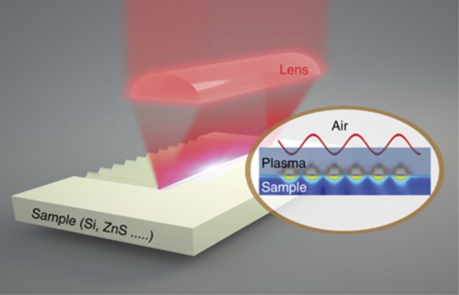
Here, we show a plasmonic nanoprinting to scale up fabrication of ripples over areas of centimeters in cross section, which are required for most of applications achieved in a practical time span of ~1 h, as shown in Figure 1. In the case of transparent materials, the debated ripple formation mechanisms are resolved showing that surface wave model of an optically excited plasma on the inner interface between the substrate and plasma, accounts quantitatively for the experimentally observed ripple period. The smallest ripple period is observed at the smallest plasma reflection and is nanoimprinted on the interface between plasma and substrate by ablation. At higher irradiance, period is decreasing due to reflectivity of top layer plasma. It is shown that previously considered conditions at the plasma–air interface Re(ε*)<−1 and the optical breakdown Re(ε*)<0 cannot explain the experimental observations. Only when Re(ε*) ≈−n2, where n is the refractive index of substrate a surface wave on the inner plasma–substrate interface accounts for observed ablated patterns and provides further insights into control of ripple formation by tailoring sub-surface electron density (hence the permittivity) to support a plasma wave for the required wavelength/period.
Figure 1.
Plasmonic nano-printing using an energy delivery by absorption of sub-surface sub-wavelength plasmons. Cylindrical lens and fast scanning improves of nano-pattern formation up to 2 × 10⁷ times as compared with the low-kHz repetition femtosecond lasers; typical aspect ratio length-to-width of the cylindrical focusing was 200.
Materials and methods
Sample fabrication
500-μm-thick p-type boron-doped single-side polished silicon wafers of <100> surface orientation (Atecom Technology Co., Ltd.) were used for large period ripple recording with 1030 nm/230 fs pulses. For sub-wavelength ripples, the β-ZnS was used. It has the complex refractive index n*=n−iκ≡(2.313−i10−4) (Ref. 26), which is related to the permittivity via  . The number density of valence electrons is NZn=1 × 1023 cm−3 considering Zn2+ valence state and 4 Zn atoms per unit cell volume a3=(0.5413 nm)3.
Optical properties
The permittivity of the optically excited plasma was calculated by27:
where τD is the Drude damping time or the electron-phonon scattering time taken equal to the optical cycle of ~3 fs at the wavelength of irradiation. This assumption is used in plasmonics28. The last term is reflecting the Drude contribution of free electrons with N0 being valance band density of electrons with N0=NZn for the results of ZnS discussed here. Details about calculations of plasma formation are presented in the Supplementary Information.
Laser fabrication
Ripples were recorded on surfaces of an absorbing Si and dielectric ZnS with 1030 nm/230 fs and 800 nm/150 fs laser pulses using cylindrical focusing (focal length<10 cm), as shown in Figure 1. Cylindrical lens was used in conjunction with standard microscope objectives for the final beam delivery onto the surface where an elongated elliptical focal spot with two major cross sections of large/small ratio larger than 10 was created. In the case of 1030 nm/230 fs pulses (Pharos, Light Conversion Ltd.), scanning at υs=(10–50) mm s−1 was used at f=(0.1–0.5) MHz laser repetition rate keeping ~15% pulse-to-pulse spot overlay (or 10 pulses per micrometer) and a typical pulse energy of Ep=8 μJ on the sample. A cylindrical lens with focal length of 80 mm was used in front of the objective lens of numerical aperture NA=0.26. Cylindrical focusing formed a dl=1.25 mm long and ds=5 μm wide line (at 1/e2 intensity level) on the surface of sample, that is, large/small≡dl/ds≈250. The ablation length was ~0.4 mm corresponding to the average 0.08 J cm−2 fluence or 3.5 W cm−2 intensity per pulse. For fabrication of patterns of ripples with continuous changes in angular orientation a λ/2 plate was synchronously rotated during linear scan (software solution by Altechna Ltd, Lithuanian). A strong air suction of ablation products was implemented; experiments were carried out in a class 1000 (ISO 6) cleanroom.
Results and discussion
Rapid fabrication of large-area structure surface by plasmonic printing
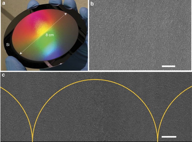
For ripples with periods close to the irradiation wavelength on the absorbing surfaces, the light interference between the incoming and the light scattered from a selvage region of surface is responsible for the ripples formation11, 12, 13. The Fourier component of the surface scattered field close to the wavelength of irradiation form the strongest interference which leads towards the ripples by ablation. Ripples are formed in a multi-shot laser exposure with surface roughness evolving as laser beam is scanned over the surface. An effective refractive index of the surface is slightly smaller compared with that of the substrate due to roughness causing a correspondingly smaller ripple periods by the mechanism presented earlier11, 12. The reduced reflectivity of ripple coated surface facilitates a stronger absorption and makes a positive feedback for ripple imprinting onto surface by ablation. An example of ripples with a close-to-the-wavelength period is shown in Figure 2 with a new record high speed of surface nanotexturing. A 4-inch wafer of Si was coated by ripples made by scanning a femtosecond laser beam with a high aspect ratio ~200 elliptical-focus. Fast linear scan of υs=5 cm s−1 was matched with a high laser repetition rate of ƒ=0.5 MHz to fulfill the required condition of a strong overlap between adjacent pulses. In comparison with 1 kHz amplified fs-laser productivity, the throughput of surface texturing is increased by ~500 × 2002=2 × 10⁷ times. For absorbing materials ripples are induced by the interference of incoming and scattered light and this method can be adapted to any absorbing surface. By utilizing cylindrical focusing and rotation of linear polarization during scanning, a complex pattern of arbitrary ripples’ orientation can be obtained, as shown in Figure 2c for the case of a circular grating.
Figure 2.
Large period ripples on an absorbing Si surface made by 1030 nm/230 fs pulses. (a) Large (indefinite) area nanotexturing of Si surface by ripples using cylindrical focusing at 0.5 MHz repetition rate and 50 mm s−1 scan speed; line focus had aspect ratio length/width≈200. (b) Closeup SEM view of the ripples; scale bar=10 μm. (c) Circular grating made by cylindircal focusing with linear polarization rotated at 2° μm−1 using a υ=0.1 mm s−1 linear scan speed; arcs mark tangential line to the ripples orientation. Scale bar=10 μm.
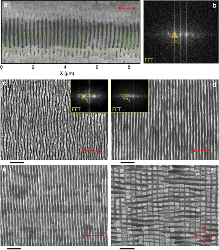
When the longer axis of an elliptical-focus is aligned to the E-field polarization of light and is perpendicular to the scan direction, ripples become more orderly. At such geometrical arrangement the ripple pattern seeded by initial pulses is self-replicated along the scan. The ordering has occurred on the absorbing Si and transparent ZnS substrates shown in Figures 2 and 3, respectively. This ordering is facilitated by simultaneous fabrication of large number of ripple periods fitting the long focus dl/Λ≥100, which could extend over tens-of-micrometers and even to centimeters by optimized focusing of laser beam, as shown in Figure 3a and 3b and Supplementary Fig. S1. Ripples are formed in a multi-pulse irradiation mode and the scanning speed, υs, controls the number of pulses per spot N=ƒ (dl/υs). As scan becomes slower, N increases and more ordered ripples are formed as revealed by Fourier analysis of the scanning electron microscopy (SEM) images (Figure 3c and 3d). This observation is consistent with recently demonstrated self-ordering due to anisotropic light scattering of defects in the sub-surface regions25. The spatial overlap of pulses at the focus defines quality of the pattern and the wider the focal region, the faster scanning speed can be used to further increase the fabrication throughput. Laser polarization (linear) determined the direction of the deep-subwavelength structures (Supplementary Fig. S2a–S2g) and can be changed during scanning to obtain rotation patterns of ripples, as shown in Supplementary Fig. S2h. The depth of ripples can be controlled by wet etching, as shown in Figure 3e. Also, two-dimensional pattern of ripples can be obtained by criss-cross scanning (Figure 3f). It is worth noting that the fabrication area is determined by the length of the linear focus and the scan length capability of the used stage rather than by other fabrication conditions. Hence, such structuring has an indefinite area texturing capability highly sought after for industrial applications.
Figure 3.
The deep sub-wavelength period ripples on a dielectric surface. SEM images of ripples on ZnS made by 500 pulse irradiation using the cylindrical lens focusing without scanning. (a) The profile line shows ripples’ continuity; (b) the FFT image (right) shows the period and the standard deviation, ±σ. Ripples recorded at the lower scan velocities had better defined period: υs=5 μm s−1 (c) and υs=0.2 μm s−1 (d). Insets c and d show FFT images corresponding to Λ=207±10 nm c and 212±25 nm d; the error ±σ margins are shown. (e) Effect of mild etching in H2SO4 (pH≈1) solution for 10 min of the pattern shown in d. (f) Two-dimensional pattern of ripples obtained by criss-cross scanning. Irradiation conditions were: pulse intensity on sample Ip=6.67 TW cm−2, wavelength of 800 nm, pulse duration of 150 fs, a cylindrical focusing, E-field was polarized perpendicular to the scan. A slight change of period for two directions is caused by an effective decrease of refractive index of the surface after the first ripples’ pattern was recorded. Scale bars c–f denote 1 μm; linear polarization is marker by arrow.
Mechanism of plasmonic printing inside volume
Formation of the sub-wavelength ripples on surfaces of dielectrics cannot be explained by the scattering theory11, 12 which accounts for the large wavelength-sized ripples on absorbing surfaces (see, Figure 2b and 2c). Coherent light scattering and resonant absorption are apparently responsible for formation of sub-surface (inner volume) ripples21, 23, 25.
Analysis of sub-wavelength ripples on transparent β-ZnS is given next based on the surface plasmon polariton (SPP) surface wave excitation at λ=800 nm wavelength for the complex refractive index n*=n−iκ≡(2.313−i10−4)26, which is related to the permittivity via n*=εr−iεi (details in Materials and Methods section and Supplementary Information).
The surface wave can be excited on a metal or plasma interface with dielectric when1: (i) the dielectric permittivity of plasma Re(εp*)<−n2 (n=1 for the interface with air) and (ii) a phase matching between the surface wave (SPP) and the wavevector |k|=2π/λ of photons is fulfilled. It is noteworthy, that the phase matching defines the polarization sensitivity of the ripple orientation. The first condition is satisfied when plasma density becomes larger than the critical density for the wavelength of excitation of Ncr=1.745 × 1021 cm−3 at λ=800 nm. At the Ncr, a solid state plasma of free electrons in conduction band drives the dielectric breakdown within few optical cycles ∼6–10 fs and creates breakdown defined by Re(ε*)≡0. The cyclic plasma frequency of electrons oscillating collectively in the driving laser light field is related to the plasma density Ne by:
where ε0 is the permittivity of vacuum, e is the electron charge, m*=m × me is the electron mass me factored by the dimensionless constant m<1, which accounts for the optical mass of electron in solid state material (m=0.4 for ZnS)29; for the breakdown plasma m*=me. Since the SPP is coherent with light and is launched during the ultra-short laser pulse before the electron-ion thermalization which occurs in several picoseconds, an unperturbed value of m=0.4 is used for simulations. The optical electron mass is defined by the electron scattering mechanisms and their concentration and temperature dependencies30.
The wave vector of the plasmon surface wave riding a conductive-dielectric interface along the linear laser polarization used in our experiments is given by31:
where k=2π/λ is the wavevector of the incident light, εd is the permittivity of the dielectric and ε* is that of plasma which was calculated for strongly excited ZnS27 (see Materials and Methods section).
The phase matching between the plasmon surface wave ks and incident light k can be achieved by either of scattering, diffraction from randomly occurring surface roughness, self-diffraction form the optically induced plasma, or via parametric scattering9, 10, 11, 12, 14, 22, 32. The parametric phase matching was demonstrated for metals22 and shows an increasing period of ripples Λ with irradiance. This proves that coupling of a normally incident focused laser beam into a surface wave takes place.
Sub-wavelength ripples are formed by accumulation of consecutive pulses and control of the absorbed energy deposition and plasma formation on the surface. A standing surface wave can be formed when ks matches the half of the Bragg wave vector of the surface structure period Λ1, 23:
Hence, the period is Λ=λs/2 for ripples due to the localized electric field enhancement and absorption occurring at the maximums of the SPP standing wave. The local irradiance is exceeding the dielectric breakdown condition Re(ε*)<0 (Ref. 23). Equation (4) describes a generic condition of wave (phonons, electrons or photons) reflection at the edge of the first Brillouin zone in a periodic structure such as a crystal for phonons and electrons or a photonic crystal for photons1. The wave reflection corresponds to the smallest wavelength of a propagating wave of the corresponding quasi-particle (phonon, electron, photon). The zone edge at the wave vector k=π/a along the direction of propagation for the pattern with a period a is equal to the wave vector, ks=2π/λs (in the considered here case of plasmon wave) yielding in the period a=λs/2. From all the other possible propagating plasmons existing on the plasma surface for which the wave vector matching can be satisfied, the smallest period exists for the standing wave which is finally imprinted on the surface. The polarization of light defines the orientation of the standing wave and determines the ripple orientation as shown in Supplementary Fig. S2.
Imprint of surface wave starts from a coherent surface excitation occurring simultaneously with the light pulse absorption followed by ablation well after the end of the laser pulse. Surface has to be excited to form plasma with Re(ε*)<−n2 to support the SPP wave on the plasma substrate surface. Any spatially small perturbation of the surface plasma will cause scattering (diffraction) with a Fourier component matching the standing SPP wave, hence, prevailing among other moving surface waves with different periods. The free carrier absorption pattern at the crests of the SPP wave makes deposition of energy, which, after the light pulse, drives the ablation of the above laying skin layer of plasma (see schematic illustration in Figure 1). When subsequent laser pulses are moving to the fresh sample surface by scanning, the existing ripples are translated over the newly excited surface which supports SPP wave of the already established period λs/2. This constitutes a self-replication and can be driven over indefinite areas similarly as shown for the large period ripples (Figure 2). Surface plasma layer has a skin depth for light intensity changing within  at plasma densities ranging from Ncr to 1022 cm3 and only 30–10 nm for the conditions of sub-wavelength ripple recording (Supplementary Fig. S4).
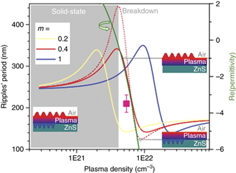
The presented above mechanism was validated experimentally. Ripples were recorded on ZnS at different pulse energies, number of overlapping pulses and compared with period of the standing surface SPP wave prediction Re(ε*)=−n2 for the (i) air–plasma (−n2=−1) and (ii) plasma–ZnS (−n2=−5.35) interfaces. Figure 4 shows the model predictions for the ripples’ period at the plasma–substrate interface. If ripples were formed via ablation on the air–plasma interface the periods around 300 nm would be expected but were never observed in experiments.
Figure 4.
Plasmonic excitation on the sub-surface plasma substrate boundary. The period of standing plasmon wave is equal to the half of the ripples’ period, Λ=λs/2 plotted for different plasma densities Ne, effective mass of electrons m*=m × me, and relaxation time of τD=3 fs close to an optical cycle (see Materials and Methods section and Supplementary Information for details). The right-side axis shows Re(ε*) dependence on Ne with horizontal arrows indicating surface wave condition at different interfaces Re(ε*)<−n2 (pictorial markers); breakdown plasma at Re(ε*)=0. The experimental point corresponding to the excitation conditions shown in Figure 3 are is presented by square marker. Note, the plasma density is calculated by Equation (1) with electron mass m=1 and vacuum wavelength λ. The period (left axis) is calculated for the plasma–substrate interface; periods on the air–plasma interface; periods on the air–plasma interface are considerably larger and are not shown.
Figure 4 shows dependence of ripple period on the plasma density calculated by Equations (3) and (4) for different optical effective mass of electron in ZnS at λ=800 nm. The experimentally observed ripples (Figure 3d and 3e) had periods Λex≈210±15 nm with a±σ span around the average estimated from FFT image analysis of SEM images. The experimentally observed ripples with periods from 120 to 220 nm fall into conditions when surface wave is formed on the inner interface between plasma and the substrate (Figure 4).
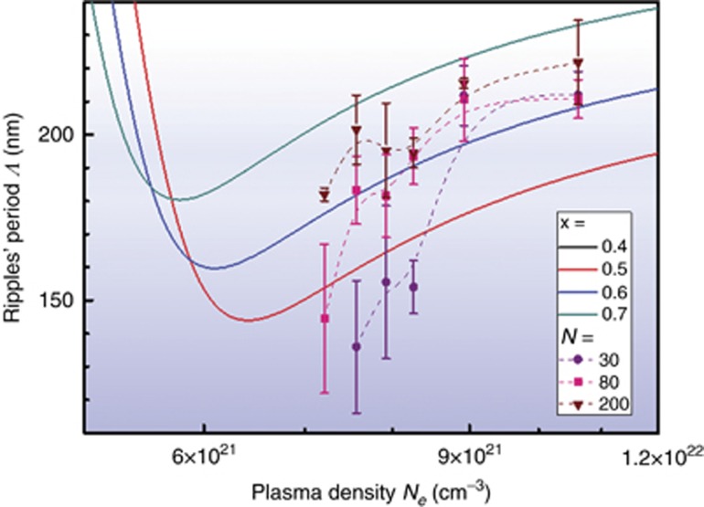
Experimentally determined ripple periods for the different number of pulses and pulse energies are plotted in Figure 5. The plasma density, Ne, was calculated from the known pulse intensity iteratively taking into account the actual time evolution of the Gaussian intensity envelop, Ip(t). The corresponding avalanche (impact), wimp(t) and multiphoton, wmpi(t), ionization rates at the instantaneous intensity were calculated together with temporal evolution of plasma screening due to the changing reflectivity, R(t), according to formulae given in Supplementary Information. This procedure allows to compare the experimental data with theoretical predictions earlier not attempted. Interestingly, the smallest periods Λ≈120 nm corresponds to the smallest reflectivity R or the lowest screening by plasma (Supplementary Figs. S3 and S4). As plasma density Ne grows (a larger pulse energy or pulse overlap), the period of ripples is evolving by prediction of the standing surface plasmon wave outlined above (Figure 4). Theoretical curves plotted for the different volume fraction, x, of air accounts for the actual reflectivity of the surface as ripples already were formed by the previous pulses, where effective permittivity is defined by that of material and air as εef (x)=(1−x)ε+xεair. The actual cross section of ripples is consistent with x=0.4–0.7 estimated by the air volume fraction of the actual ripples16. For the smaller number of pulses, N, per focal spot, smaller Λ were observed and corresponded to ripples with x=(0.4–0.5) judging from SEM images. For the larger N, a larger portion of surface was ablated and ripples had an air fraction x=(0.6–0.7). For the larger x values, surface becomes more anti-reflective and larger ripple periods are observed for the larger pulse energy due to lower electronic excitation reaching the plasma–substrate interface (a stronger plasma screening at the top air–plasma interface occurred).
Figure 5.
The ripple period, Λ, vs plasma density Ne calculated for different pulse energies and number of the overlapping pulses per spot, N. Theoretical curves are plotted for different ZnS fractions, (1−x), of an effective surface permittivity to account for surface ripple formation and the corresponding change the surface reflectivity; x is the fraction of air.
The tendency Λ∝N was confirmed and can be rationalized by a defect accumulation effect which is reflected in an increasing absorption Im(ε) of the substrate (Supplementary Figs. S3 and S4). This augmented absorption eventuates in higher values of Ne and Λ since the higher plasma densities at the air–plasma region are screening excitation at the plasma–substrate interface causing the larger Λ values as observed in experiment (Figure 5).
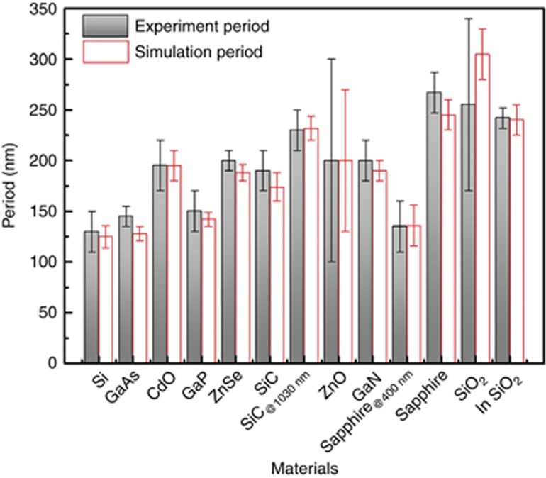
The nanoplasmonic imprinting model was also checked on other materials and compared with the reported experimental results. Shown in Figure 6 and Supplementary Table S1, deep-subwavelength structures were simulated according to the experimentally reported conditions on silicon33, GaAs34, CdO35, GaP34, ZnSe36, SiC37, ZnO38, GaN23, sapphire39, 40 and silica41, 42, and predictions of herein outlined model had a good correspondence with the experimental observations (SiC and sapphire were structured at different wavelengths). The period calculated for silica (x=0) coincided with experimental results and validated the plamonic nano-imprinting model as universal to explain the origin of deep-subwavelength ripples.
Figure 6.
Deep-subwavelength Period simulation for different materials. Λ denotes the structure period in experiment while Λ_S is the simulation results.(Experimental data of silicon33, GaAs34, CdO35, GaP34, ZnSe36, SiC37, ZnO38, GaN23, sapphire39, 40 and silica41, 42).
Conclusions
It is demonstrated that indefinite areas can be nanotextured with ripples with limitation defined only by surface processing speed proportional to the laser repetition rate. The use of a cylindrical focusing facilitates large area fabrication of ripples as shown for Si. Surface texturing at ~10 cm s−1 speed required by industry43 is already a feasible technology as shown here by ~107 times improvement in surface texturing speed as compared with a low-kHz repetition laser fabrication. Augmented fabrication throughput in surface nanotexturing will impact applications in sensing, solar energy, fuel cells44, 45.
It is determined that sub-wavelength ripples are formed via plasmonic nano-imprinting of the standing wave with period defined by the plasma density at the interface with the dielectric substrate. The model accounting for the actual electron generation rate simultaneously with evolution of plasma reflectivity is validated for ZnS and confirmed by experimental results on other materials. This shows how an absorptive nature of surface plasmonics waves is utilized for energy deposition with nanoscale precision and becomes an advantage in plasmonic nano-printing.
The presented analysis of ripple formation can be used to refine intricate electron scattering constants and their temperature and concentration dependencies in a strongly nonuniform and periodic density plasma which are currently known only approximately.
Acknowledgments
HBS thanks the support by the National Key R&D Program of China (No.2017YFB1104600) and the National Natural Science Foundation of China (NSFC) 61590930, 91423102, 91323301, and 61435005. SJ is thankful to Gintas Slekys for the partnership project with Workshop of Photonics Ltd. on industrial femtosecond laser fabrication. Partial support via ARC Discovery DP170100131 grant is acknowledged. We are grateful to Professors Eugene G Gamaly and Kenzo Miyazaki for discussion on laser ablation.
Footnotes
Note: Supplementary Information for this article can be found on the Light: Science & Applications’ website(http://www.nature.com/lsa).
The authors declare no conflict of interest.
Supplementary Material
References
- Barnes WL, Dereux A, Ebbesen TW. Surface plasmon subwavelength optics. Nature 2003; 424: 824–830. [DOI] [PubMed] [Google Scholar]
- Kuznetsov AI, Miroshnichenko AE, Fu YH, Zhang JB, Luk'Yanchuk B. Magnetic light. Sci Rep 2012; 2: 492. [DOI] [PMC free article] [PubMed] [Google Scholar]
- Yu NF, Genevet P, Kats MA, Aieta F, Tetienne JP et al. Light propagation with phase discontinuities: generalized laws of reflection and refraction. Science 2011; 334: 333–337. [DOI] [PubMed] [Google Scholar]
- Lin DM, Fan PY, Hasman E, Brongersma ML. Dielectric gradient metasurface optical elements. Science 2014; 345: 298–302. [DOI] [PubMed] [Google Scholar]
- Valentine J, Zhang S, Zentgraf T, Ulin-Avila E, Genov DA et al. Three-dimensional optical metamaterial with a negative refractive index. Nature 2008; 455: 376–379. [DOI] [PubMed] [Google Scholar]
- Prodan E, Radloff C, Halas NJ, Nordlander P. A hybridization model for the plasmon response of complex nanostructures. Science 2003; 302: 419–422. [DOI] [PubMed] [Google Scholar]
- Kuznetsov AI, Miroshnichenko AE, Brongersma ML, Kivshar YS, Lukyanchuk B. Optically resonant dielectric nanostructures. Science 2016; 354: aag2472. [DOI] [PubMed] [Google Scholar]
- Wang X, Deng Y, Li QT, Huang YJ, Gong ZL et al. Excitation and propagation of surface plasmon polaritons on a non-structured surface with a permittivity gradient. Light Sci Appl 2016; 5: e16179, doi:10.1038/lsa.2016.179. [DOI] [PMC free article] [PubMed] [Google Scholar]
- Birnbaum M. Semiconductor surface damage produced by ruby lasers. J Appl Phys 1966; 36: 3688–3689. [Google Scholar]
- Zhou GS, Fauchet PM, Siegman AE. Growth of spontaneous periodic surface structures on solids during laser illumination. Phys Rev B 1982; 26: 5366–5381. [Google Scholar]
- Sipe JE, Young JF, Preston JS, van Driel HM. Laser-induced periodic surface structure. I. Theory. Phys Rev B 1983; 27: 1141–1154. [Google Scholar]
- Young JF, Preston JS, van Driel HM, Sipe JE. Laser-induced periodic surface structure. II. Experiments on Ge, Si, Al, and brass. Phys Rev B 1983; 27: 1155–1172. [Google Scholar]
- Jiang L, Han WN, Li XW, Wang QS, Meng FT et al. Crystal orientation dependence of femtosecond laser-induced periodic surface structure on (100) silicon. Opt Lett 2014; 39: 3114–3117. [DOI] [PubMed] [Google Scholar]
- Akhmanov SA, Emel'yanov VI, Koroteev NI, Seminogov VN. Interaction of powerful laser radiation with the surfaces of semiconductors and metals: nonlinear optical effects and nonlinear optical diagnostics. Sov Phys Usp 1985; 28: 1084–1124. [Google Scholar]
- Sugioka K, Cheng Y. Ultrafast lasers—reliable tools for advanced materials processing. Light Sci Appl 2014; 3: e149, doi:10.1038/lsa.2014.30. [Google Scholar]
- Buividas R, Mikutis M, Juodkazis S. Surface and bulk structuring of materials by ripples with long and short laser pulses: recent advances. Prog Quantum Electron 2014; 38: 119–156. [Google Scholar]
- Malinauskas M, Žukauskas A, Hasegawa S, Hayasaki Y, Mizeikis V et al. Ultrafast laser processing of materials: from science to industry. Light Sci Appl 2016; 5: e16133, doi:10.1038/lsa.2016.133. [DOI] [PMC free article] [PubMed] [Google Scholar]
- Liu PJ, Jiang L, Hu J, Zhang S, Lu YF. Self-organizing microstructures orientation control in femtosecond laser patterning on silicon surface. Opt Express 2014; 22: 16669–16675. [DOI] [PubMed] [Google Scholar]
- Ozkan AM, Malshe AP, Railkar TA, Brown WD, Shirk MD et al. Femtosecond laser-induced periodic structure writing on diamond crystals and microclusters. Appl Phys Lett 1999; 75: 3716–3718. [Google Scholar]
- Shimotsuma Y, Kazansky PG, Qiu JR, Hirao K. Self-organized nanogratings in glass irradiated by ultrashort light pulses. Phys Rev Lett 2003; 91: 247405. [DOI] [PubMed] [Google Scholar]
- Huang M, Zhao FL, Cheng Y, Xu NS, Xu ZZ. Origin of laser-induced near-subwavelength ripples: interference between surface plasmons and incident laser. ACS Nano 2009; 3: 4062–4070. [DOI] [PubMed] [Google Scholar]
- Sakabe S, Hashida M, Tokita S, Namba S, Okamuro K. Mechanism for self-formation of periodic grating structures on a metal surface by a femtosecond laser pulse. Phys Rev B 2009; 79: 033409. [Google Scholar]
- Miyazaki K, Miyaji G. Nanograting formation through surface plasmon fields induced by femtosecond laser pulses. J Appl Phys 2013; 114: 153108. [Google Scholar]
- Liao Y, Ni JL, Qiao LL, Huang M, Bellouard Y et al. High-fidelity visualization of formation of volume nanogratings in porous glass by femtosecond laser irradiation. Optica 2015; 2: 329–334. [DOI] [PubMed] [Google Scholar]
- Rudenko A, Colombier JP, Itina TE. From random inhomogeneities to periodic nanostructures induced in bulk silica by ultrashort laser. Phys Rev B 2016; 93: 075427. [Google Scholar]
- Refractive index database. Available from: http://refractiveindex.info/?group=CRYSTALS&material=ZnS (accessed 27 December 2016).
- Sokolowski-Tinten K, von der Linde D. Generation of dense electron-hole plasmas in silicon. Phys Rev B 2000; 61: 2643–2650. [Google Scholar]
- Maier SA. Plasmonics: Fundamentals and Applications. New York: Springer; 2007. [Google Scholar]
- Pankove JI. Optical Processes in Semiconductors. New York: Dover Publications, Inc.; 1975. [Google Scholar]
- Gamaly E. Femtosecond Laser-Matter Interactions: Theory, Experiments and Applications. Singapore: Pan Stanford Publishing Pte, Ltd.; 2011. [Google Scholar]
- Born M, Wolf E. Principles of Optics: Electromagnetic Theory of Propagation, Interference and Diffraction of Light. 7th ed. Cambridge: Cambridge University Press; 2002. [Google Scholar]
- Hashida M, Ikuta Y, Miyasaka Y, Tokita S, Sakabe S. Simple formula for the interspaces of periodic grating structures self-organized on metal surfaces by femtosecond laser ablation. Appl Phys Lett 2013; 102: 174106. [Google Scholar]
- Straub M, Afshar M, Feili D, Seidel H, Köenig K. Periodic nanostructures on Si(100) surfaces generated by high-repetition rate sub-15 fs pulsed near-infrared laser light. Opt Lett 2012; 37: 190–192. [DOI] [PubMed] [Google Scholar]
- Wang C, Huo HB, Johnson M, Shen MY, Mazur E. The thresholds of surface nano-/micro-morphology modifications with femtosecond laser pulse irradiations. Nanotechnology 2010; 21: 075304. [DOI] [PubMed] [Google Scholar]
- Choi SG, Zuniga-Perez J, Muñoz-Sanjosé V, Norman AG, Perkins CL et al. Complex dielectric function and refractive index spectra of epitaxial CdO thin film grown on r-plane sapphire from 0.74 to 6.45 eV. J Vac Sci Technol B 2010; 28: 1120–1124. [Google Scholar]
- Wang ST, Feng GY, Zhou SH. Microsized structures assisted nanostructure formation on ZnSe wafer by femtosecond laser irradiation. Appl Phys Lett 2014; 105: 253110. [Google Scholar]
- Ričardas B, Lorenzo R, Remigijus Š, Tadas K, Gintas Š et al. Mechanism of fine ripple formation on surfaces of (semi)transparent materials via a half-wavelength cavity feedback. Nanotechnology 2011; 22: 055304. [DOI] [PubMed] [Google Scholar]
- Bonse J, Rosenfeld A, Krüger J. Femtosecond laser-induced periodic surface structures: recent approaches to explain their sub-wavelength periodicities. Proc SPIE 2011; 7994: 79940M. [Google Scholar]
- Buividas R, Rekštytė S, Malinauskas M, Juodkazis S. Nano-groove and 3D fabrication by controlled avalanche using femtosecond laser pulses. Opt Mater Express 2013; 3: 1674–1686. [Google Scholar]
- Juodkazis S, Nishimura K, Misawa H. In-bulk and surface structuring of sapphire by femtosecond pulses. Appl Surf Sci 2007; 253: 6539–6544. [Google Scholar]
- Bhardwaj VR, Simova E, Rajeev PP, Hnatovsky C, Taylor RS et al. Optically produced arrays of planar nanostructures inside fused silica. Phys Rev Lett 2006; 96: 057404. [DOI] [PubMed] [Google Scholar]
- Sun Q, Liang F, Vallée R, Chin SL. Nanograting formation on the surface of silica glass by scanning focused femtosecond laser pulses. Opt Lett 2008; 33: 2713–2715. [DOI] [PubMed] [Google Scholar]
- Cary HB, Helzer SC. Modern Welding Technology. 6th ed. New Jersey: Upper Saddle River; 2005. [Google Scholar]
- Chou A, Jaatinen E, Buividas R, Seniutinas G, Juodkazis S et al. SERS substrate for detection of explosives. Nanoscale 2012; 4: 7419–7424. [DOI] [PubMed] [Google Scholar]
- Buividas R, Stoddart PR, Juodkazis S. Laser fabricated ripple substrates for surface-enhanced Raman scattering. Ann Phys 2012; 524: L5–L10. [Google Scholar]
Associated Data
This section collects any data citations, data availability statements, or supplementary materials included in this article.


