Abstract
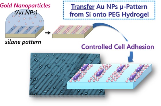
Amino-silanization of silica-based substrates has proven to be effective in guiding the immobilization of citrate-stabilized Au NPs in a good, homogeneous fashion. This accomplishment has formed the basis of fabricating micropatterns of Au NPs on such substrates by patterning of oxidized silicon wafers with (3-aminopropyl)trimethoxysilane (amino-silane) using the microcontact printing (μCP) process. This micropattern of amino-silane is used to specifically adsorb Au NPs. To avoid unspecific adsorption to the nonsilanized areas on the silicon wafers, the nonstamped areas were backfilled with self-assembled monolayers of organosilanes, for example, with methyl- or perfluoro-end-groups. Finally, after having fabricated a micropattern of Au NPs on silicon wafers, the Au NP patterns were transferred onto poly(ethylene glycol) hydrogels by our newly developed procedures, and on these nanocomposite materials, controlled cell adhesion has been achieved. Furthermore, these materials are great candidates for plasmon-based biosensor applications and also for various medical applications, such as for drug delivery systems or photothermal therapies.
Introduction
Surface modifications are of great importance in various research and applied fields, ranging from chemistry, mechanical, or electrical engineering to industry.1−5 Hereby, the original or intrinsic property of a material, such as the reactivity, wettability, hydrophilicity, or biological activity, can be changed, specifically tuned and adjusted to conform to the applied environment. Especially self-assembled monolayers (SAMs) of organosilanes (silanization) have offered a great opportunity for achieving that goal.6,7 Silanization is a method for functionalizing the surface of a substrate using organosilane molecules, which have general molecular structures of RSiX3, R2SiX2, or R3SiX, hereby X is chloride or alkoxy-group and R is typically a hydrocarbon chain with a functional group. After hydrolysis and condensation reactions, the molecules are covalently attached to the surface and effectively modify its chemical properties.6,8−10 For instance, using SAMs in biological or biomedical fields, attractive or repulsive interactions of proteins, DNA, or anti-bodies with the biointerface can be manipulated to obtain the desired biointeraction.11,12
Of particular interest for biomaterials applications are surface modifications involving poly(ethylene glycol) (PEG), a highly hydrophilic, nontoxic, and nonimmunogenic polymer.13,14 PEG monolayers have demonstrated to be intrinsically nonadhesive toward proteins and consequently also nonadhesive toward whole cells; they are highly inert toward biomolecular interactions.15 Those properties make PEG in SAMs on silicon or glass surfaces especially attractive as inert backgrounds for studying specific biointeractions. Furthermore, by combining SAM technology with lithographic methods (vide infra), nano- or micro-patterns on surfaces can be fabricated.7,16−18 Micro- or nano-patterning of surfaces is of great interest in many fields, not restricted to biological applications, such as micro- or nano-electronics,19−21 switchable systems,22 biosensors, and nano-biotechnology.23
PEG with reactive end-groups can be easily cross-linked, for example, by photoinitiated radical cross-linking or other chemical cross-linking procedures, to form hydrogels.24,25 Hydrogels are three-dimensional networks of hydrophilic polymers (macromonomers) which can absorb huge amounts of water without being dissolved. By variation of the chain-length of the macromonomers, using additional cross-linkers or changing the chemical compositions the elastic, physical, or chemical properties of the hydrogels can be specifically varied, which make them highly versatile materials that find numerous applications such as in care products,26,27 contact lenses,28 drug delivery,29 or tissue engineering.30 Even more than PEG SAMs on hard (glass) substrates, soft PEG hydrogels are an ideal, inert background that suppresses nonspecific interactions. This enables the introduction of specific binding sites onto the surface of PEG hydrogels at designed locations and in an optimal density for studying specific biointeraction and manipulating31−33 In the past years, we have exploited several strategies to enable adhesion, spreading, and migration of fibroblast cells on intrinsically nonadhesive PEG-hydrogels. We have fabricated topographic, elastic, and chemical patterns on the hydrogels’ surface, both at the micro- and nano-scale and achieved great control over the cellular responses.34−44
One example of chemical modification is the incorporation of nanoparticles for achieving nanocomposite materials.45 Among them, especially for application in biological or biomedical fields, Au NPs are highly desired because of their little toxicity and various possibilities to synthesize them with different sizes, shapes, and surface molecules, where the optical and chemical properties can be also varied.46 We and others have discovered that the decoration of PEG surfaces with Au NPs is an effective way to study and control specific biointeraction and cell adhesion. Hereby, not only the size and shape but also the density and naturally the surface chemistry of the Au NPs are variable parameters by which the biointerfaces can be tuned.
For example, Spatz et al. have reported extensively about their elegant studies of how the interparticle distance between Au NPs (immobilized on PEG-coated glass) should match the nanoscale distribution of the integrin receptors on the cell membrane.47−49 To ensure selective cell adhesion to the nanoscopic anchoring sites, they functionalized the Au NPs with a cell adhesive peptide, that is, RGD. They also demonstrated that they could transfer Au NPs from hard substrates to soft PEG hydrogels by functionalizing the Au NPs with reactive (e.g., acrylate) groups that covalently bound to the PEG-macromonomers.50 Notwithstanding the quality of their results and the great insight their studies have yielded, their procedures involved partly complicated functionalization steps with delicate and expensive molecules.
We have recently demonstrated that we can transfer as-synthesized, citrate-capped Au NPs to the surface of PEG hydrogels without the need for any surface modification of the Au NP surface.39,41 Obviously, the chemical modification of the hydroxyl end groups on the PEG polymer chains by thiol groups was found to make the transfer of the Au NPs especially efficient (transfer efficiency of >98% is feasible).39 But also nonfunctionalized PEG gels, for example, UV-cured gels from PEG diacrylate, have been successfully employed to peel off Au NPs when taking advantage of the swelling ability of the hydrogels. We call this process “wet deprinting”, which we can also perform in a micro-patterned fashion, hence “wet μ-CdP”.41
Furthermore, we observed effective cell adhesion on our nonfunctionalized Au NPs. This has inspired us to develop many more of such unique nano- and micro-patterning procedures for patterning Au NPs on PEG hydrogels with the aim of locally controlling the cell adhesion.39−43
Concerning the sizes of the cells, that is, ∼10–20 μm, the controlled dimensions of the micro-sized patterns are of great importance for the spatial control of cell adhesion. While photo- and e-beam lithography are versatile micro- and nano-fabrication techniques, they are either limited in the achievable feature size or become slow and costly whenever smaller features are aimed at.51−53 Those drawbacks are effectively overcome by the invention of soft lithography. That is why we take advantage of established, effective soft-lithographic methods, such as micro-contact printing (μCP),7 as developed by Whitesides et al., or the nano-transfer printing54 method from Rogers et al. in combination with sinusoidal or wrinkled stamps.55 Nevertheless, we also further developed our own technologies, such as micro-contact deprinting (μ-CdP) via heating of the stamp above the glass transition temperature56 or using chemically or elastically modified hydrogels,40 wet micro-contact deprinting (wet μ-CdP),41 and nanocontact transfer using nanowrinkled poly(dimethylsiloxane) (PDMS) stamps.42
In this work, we present yet another method, taking advantage of μCP and our own transfer methods. First, micropatterns of amino-silanes are printed on silicon wafers, which ensure the spatially controlled immobilization of citrate capped Au NPs following the process of Li et al.18 and the remaining nonstamped area are backfilled with another silane type (e.g., with methyl-, or perfluoro-end-groups), which effectively avoid Au NP attachment.57 In the second step, the Au NP pattern is transferred onto the PEG hydrogel surface by one of our recently developed transfer methodologies, in particular the “dry” transfer using thiolated PEG gels and the wet deprinting approach.39−43
These novel micropatterned nanocomposite substrates are ultimately applied in cell culture studies with the aim of controlling selective cell adhesion of fibroblasts to the micropatterns of Au NPs.
Results and Discussion
In this work, a two-step process is used to achieve a micropattern of Au NPs on the surface of PEG-based hydrogels (Scheme 1). First, a micropattern of Au NPs on the surface of a silicon wafer was achieved, and then this Au NP pattern was transferred as a whole onto the surface of PEG hydrogels by our recently developed transfer techniques.
Scheme 1. (a) Process of Successive Micropatterning with Different Silanes for Micropatterning of Au NPs on Silicon Wafers; (b) Transfer of Au NP Pattern from Silicon Surfaces onto PEG-Based Hydrogels.
The first challenge was to achieve a good pattern on the silicon wafer which was done via μCP of (3-aminopropyl)trimethoxysilane (amino-silane) on the surface of oxidized silicon wafers. This micropattern of amino-silane was used to specifically adsorb Au NPs.18 Unspecific adsorption to nonsilanized areas on the silicon wafer had been observed and therefore it was of interest to solve this problem by efficient backfilling of the nonstamped area with SAMs of organosilane,57,58 for example, with methyl- or perfluoro-end-groups, which provide a certain inertness to these area and avoid unspecific Au NP adhesion (Scheme 1a). Finally, after achieving a relatively good pattern on the silicon wafer, the Au NPs were transferred onto the surface of PEG-based hydrogels (Scheme 1b) where cell adhesion could be locally controlled.
In detail, first of all, amino-silane molecules were printed on the surface of the silicon wafers using PDMS stamps exhibiting microsized topographic patterns (Figure 1a).18 The microcontact printed amino-silane layer is shown in the atomic force microscopy (AFM) image in Figure 1b,c. Hereby, the pattern size for the master was (20 μm–10 μm–5 μm), that is the printed (contacted) area had a width of 10 μm and a distance of 20 μm, which can be well recognized in the AFM height image and in the cross section profile in Figure 1b,c. In the cross section profile in Figure 1c, a height of around 0.7–1.8 nm for the amino-silane layer was observed. The height of 0.7 nm is comparable with the literature values for a monolayer of amino-silane on surfaces.
Figure 1.
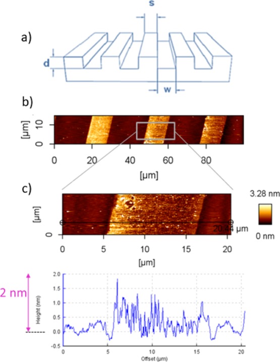
(a) Structure of micropattern with 3-numeric codes; w–s–d = width of the grooves–spacing between the grooves–depth of the grooves of a relief pattern; (b,c) AFM height images and cross section profile of amino-silane-micro-pattern on silicon wafer; pattern size of the used stamp (20 μm–10 μm–5 μm).
In Figure 2, the AFM height images and cross section profiles of the amino-silane pattern; (a) before backfilling and (b) after backfilling with octadecyl-silane are presented. The height profiles show the heights on the free or backfilled areas: in Figure 2a the height profile of the nonstamped area on the oxidized silicon-wafer show a height of around 0.1–0.5 nm and an rms roughness of 123 pm, whereas after backfilling the height profile was increased to around 2–5 nm and an rms roughness of 1.1 nm was measured. For a monolayer of octadecyl-silane, a height value of 2.65–2.76 nm was reported,58−61 that means the backfilled surface was either a mono or a double layer.
Figure 2.
AFM height images and cross section profiles of (a) amino-silane micro-pattern on silicon wafer before backfilling; (b) amino-silane backfilled with octadecyl-silane. The cross section profiles were measured on the (a) free or (b) backfilled area. Pattern size of the used stamp (20 μm–10 μm–5 μm).
On this micropattern of amino-silane silicon wafer, Au NPs were deposited, which is shown in the scanning electron microscopy (SEM) images in Figure 3; there, in Figure 3a, a pattern of 10 μm wide brighter lines and 20 μm wide, comparably darker lines are recognizable. The brightness of the SEM results was evoked by the high electron densities of the Au NPs. In Figure 3b,c which were magnified images, the Au NPs were clearly visible. From these results, it is visible that the Au NPs were found over the whole sample but with different packing densities. On the amino-silane lines, the Au NPs were more densely packed than on the oxidized silicon wafer.
Figure 3.

SEM images of Au NP coating on amino-micro-patterned silicon wafer; pattern size of the used stamp (20 μm–10 μm–5 μm): scale bars: (a) 40 μm; (b) 4 μm; (c) 1 μm.
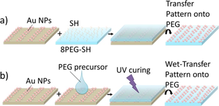
This pattern of differently densely packed Au NPs was then transferred onto hydrogels by merely contacting the free standing hydrogel with the Au NP pattern on the silicon wafer (Schemes 1b and 2).
Scheme 2. Au NP Pattern Transfer from Silicon Wafers onto (a) 8PEG-SH Hydrogel; (b) Nonfunctional PEG Hydrogels via Wet-Deprinting Process.
In this work, two different hydrogels were used to transfer the Au NPs; (a) onto free standing 8PEG-SH hydrogels or (b) onto nonfunctional PEG hydrogels by virtue of swelling the UV-cured film before peeling it off. Details can be found in the Experimental Section (vide infra).
Starting off with the process depicted in Scheme 2a, that is, using thiolated 8PEG hydrogels, in Figure 4 SEM images of the transferred Au NPs on 8PEG hydrogel are shown. In analogy to the Au NP patterns on silicon wafer before transfer, the Au NPs on the PEG surface were found over the whole sample, while exhibiting different packing densities (see Figure 4c,d). The area transferred from the nonstamped area was relatively more loosely packed (Figure 4c) and from amino-silane layer were more densely packed with Au NPs (Figure 4d); that is the original pattern was effectively transferred onto the surface of PEG hydrogel.
Figure 4.
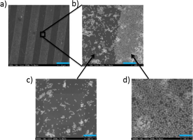
SEM images of Au NPs transferred on 8PEG-SH hydrogel. Scale bars: (a) 20 μm; (b) 400 nm; (c) 400 nm; (d) 200 nm.
To achieve even more clearly defined patterns of Au NP and non-Au NP areas on the silicon surface, the process was further improved by backfilling of the remaining, nonstamped areas with another type of silane, which should not bind or interact with Au NPs. While coating of a surface with amino-silanes caused highly densely packed citrate-capped Au NPs39,40,42 because of electrostatic interactions, backfilling of the remaining area with other silanes (e.g., with end groups: −CH3, −CF3) would expectedly minimize the adhesion of citrate-capped Au NPs. For that the remaining areas were silanized either with octadecyl-silane using the liquid silanization process or with perfluoro-silane via the vapor-silanization method.
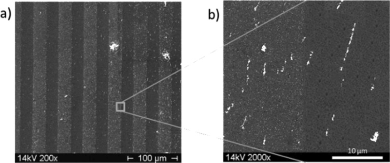
In Figure 5, SEM images of the Au NP-coated silicon wafer on amino- and octadecyl-silane lines are shown. Again, a high packing density of Au NPs on amino-lines and quite few Au NPs on the surface of the octadecyl-silane-lines were visible. Some brighter features on the SEM images were observable as well, which were presumably agglomerated Au NPs attached on the surface of the sample. Such agglomeration can be either due to aging effects of the Au NPs in the solution or due to the irregular distribution of the of amino-silane SAM. These agglomerations of Au NPs were also found on octadecyl-silane layers, which might be caused when the whole backfilled surface was not completely covered by octadecyl-silane and consequently the oxidized surface might be not absolutely made inert toward Au NPs attachment.
Figure 5.
SEM images of Au NP coating on amino- and octadecyl-silane pattern. Scale bars: (a) 100 μm; (b) 10 μm.
In Figure 6, AFM height images with a cross section profile of the deposited Au NPs on the amino- and octadecyl-silane-layers are shown; hereby, in accordance with the observations of the SEM results, a high density of Au NPs on amino-silane layer and only few particles on the octadecyl-silane-layer are observable. The height profiles show a height of around 20–50 nm in a large area on the amino-silane layer with some agglomerations. The hereby used Au NPs had a size of 20 nm, while a height of 40–50 nm was measured by AFM. In these cases, probably even double Au NP layers might be formed on the amino-silane surface or there might be an effect of side or vertical polymerizations of SAMs which increased the height profile and even lead to agglomeration effects of the Au NPs.62
Figure 6.
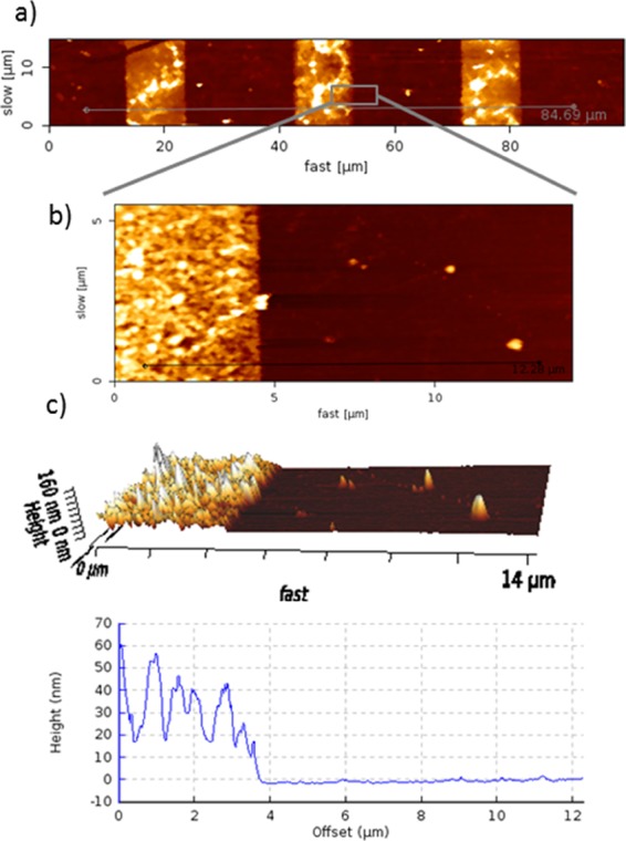
AFM (a,b) height images and (c) 3D image and cross section profile of amino-silane and octadecyl-silane pattern after Au NPs coating.
Perfluoro-silanes are known for their hydrophobicity and chemically inert characteristics; therefore, they were also used as coating for our silicon masters to keep them clean and nonreactive toward the stamps or replica molds. These inert characteristics were also applied for patterning of silane agent methods for having a nonreactive area or nonbinding sites for Au NP adhesions besides the well-reactive amino-silane lines. Hereby, the amino-silane patterned silicon wafer was backfilled with perfluoro-silane using the vapor-silanization process and on this wafer, Au NPs were deposited, which is shown in Figure 7.
Figure 7.
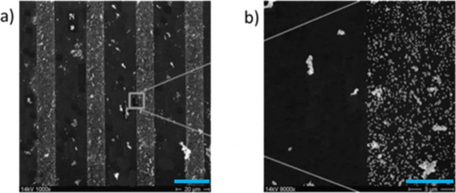
SEM images of Au NPs coating on amino- and perfluoro-silane-pattern. Scale bars: (a) 100 μm; (b) 10 μm.
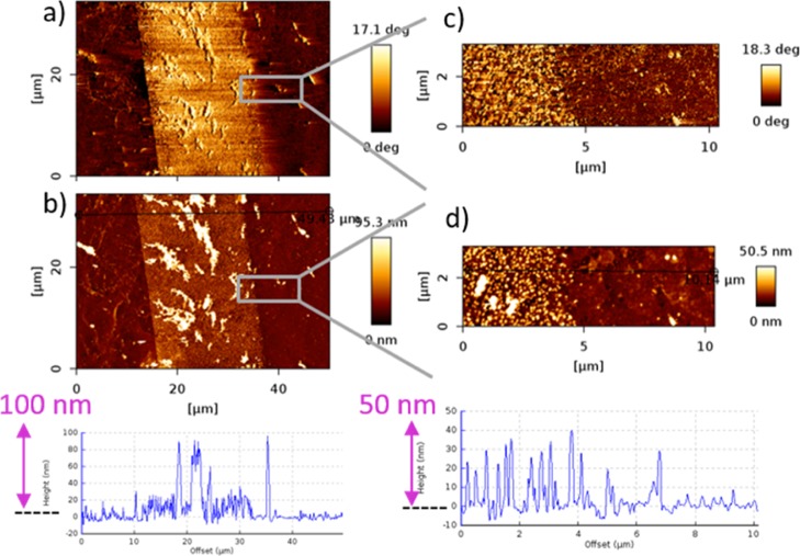
In Figure 7, similar to the backfilling reaction of amino-silane patterns with octadecyl-silane, highly dense Au NPs on the amino-silane layer and a few agglomerated particles over the whole surface of amino- and perfluoro-silane is observable via SEM images. Further Au NP coating on amino- and perfluoro-pattern is shown via AFM height images, cross section profiles, and phase images in Figure 8. Hereby, the stamping area for amino-silane had a width of 20 μm, which is observable in the phase image in Figure 8a as a brighter line in a darker surrounding, which represented the perfluoro-silane layer. On the perfluoro-silane layer, some brighter features are also visible, which can be also recognized in the height image in Figure 8b as agglomerations of Au NPs with heights of around 100 nm. Some more agglomerations with around the same height sizes are also visible on the amino-silane lines. On the amino-silane lines the distribution of the 20 nm Au NPs as a monolayer exactly on the amino-silane stamped area are visible. This can be clearly seen in Figure 8c,d, which are phase and height images and a cross section profile of an enlarged view of an edge of the stamped and nonstamped area from Figure 8b. In the phase image, the amino-templated line, which contained the Au NPs is recognized by the bright color, whereas the backfilled part is seen in darker color. The height image and profile exhibited a height of 18–40 nm for the Au NP sizes; the size distribution could be due to the polydispersity of the synthesized Au NPs.
Figure 8.
(a) AFM phase image; (b) height image and cross section profile; (c) magnified phase image; and (d) magnified height image and cross section profile.
These Au NP patterns were subsequently transferred onto PEG hydrogel surfaces, in this case using the procedure as schematically depicted in Scheme 2b, namely, by virtue of swelling a UV-cured PEG film before peeling it off. In recent years, we have worked extensively with such PEG hydrogels and know from our experience that they are highly cytocompatible, while they are intrinsically nonadhesive to proteins and cells.
Eventually, cell adhesion studies on these hydrogels with Au NP micro-lines were performed. As observed by optical microscopy, already after 2 h of cultivation time of murine fibroblast cells, the cells were accumulating on the Au NP patterns. Apart from the cells, the pattern can be recognized in the form of darker and brighter lines. Here, the darker lines correspond to Au NP lines and the brighter lines are the pure PEG hydrogel. In some cases, small irregular black dots were visible, which are probably agglomerations of Au NPs, which were previously observed on the silicon surfaces and that were transferred onto the hydrogel as well.
Analyzing the behavior of cell adhesion on the patterned surface after 24 h (Figure 9), it can be recognized that the cells were selectively adhering on the Au NP lines and most of them were aligning following the line pattern (marked by blue ellipses). Some other cells were not directly adhering on the Au NP lines but were either bridging over the PEG lines (green circle) or residing as round shapes on the PEG area (pink ellipse on the right).
Figure 9.
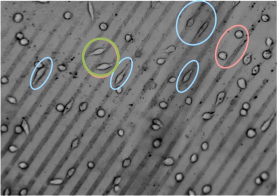
Optical micrograph of cell adhesion on Au NP-patterned PEG hydrogel.
Further qualitative analysis of the cellular behavior (Table S1) supported the qualitative statements; (i) 86 ± 5% of cells were attached on the Au NP lines in total (including the bridging cells), and (ii) 71 ± 8% of the cells were aligning on the Au NP lines following the pattern direction at an angle of 0°–10°.
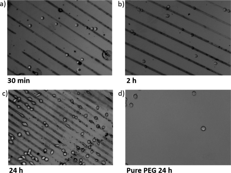
To get an insight in the timescale of the selective cell adhesion, we observed the cell culture at different time points, that is, 30 min, 2 h, and 24 h. Figure 10 shows the time dependency of the cell adhesion to the patterned substrates.
Figure 10.
Optical micrographs of cell culture (a–c) on Au NP micropattern on PEG hydrogels with different cultivation times and (d) on pure PEG after 24 h.
Figure 10a is an image after 30 min of cultivation time. At this early time point, the cells had round shapes and were only slightly attaching on the surface without showing any preference; in addition to residing on the Au NP lines, many cells were seen on the pure PEG lines as well. After 2 h of cultivation time, some lamellipodia of the cells could be observed and more than half of the total amount of cells (∼60%) were found on Au NP lines (see Figure 10b). At the end point of the observation (after 24 h of cultivation), up to 90% of the cells were on the Au NP lines, and were stretched along the direction of the lines, which is shown in Figure 10c. Again, some cells were oriented rather perpendicularly to the Au NP lines, establishing contacts to two parallel lines and bridging over the pure PEG hydrogel line. As a control, on pure PEG hydrogel surfaces cells were not adhering at all (Figure 10d).
Using this printing-based patterning method, any pattern size and shape can be obtained, depending on the design of the (silicon) master and relying on the integrity of the PDMS stamp. This is of great advantage for applications in which, for example, curved or sharp-cornered edges are desired instead of linear and right-cornered ones. For our eventual aim of controlling cell adhesion, spherical shapes are also interesting features. Therefore, as an example to micropattern Au NPs on PEG hydrogels in spherical-shaped patterns, we prepared a stamp with cylindrical pillar-like topographic patterns. The resulting equidistant dots (of ∼50 μm in size) of Au NPs on the hydrogel surface are shown in Figure S2. By tuning the sizes and shapes of the dots with respect to the sizes of the cells, control over selective cell adhesion can be obtained, so that single cells can be distinctly separated and studied.
Conclusions
In this work a novel, cheap, and fast surface micropatterning procedure based on soft lithography for micropatterning of Au NPs first on silicon wafers were proposed, which were then transferred onto PEG-based hydrogels for studying cellular interactions. For this approach, well-defined line pattern of Au NPs on silica surfaces as the first step of the process was generated. This was achieved with two different patterning principles relying on soft lithography techniques. In both cases, SAMs of (3-aminopropyl)trimethoxysilane (amino-silane) served as platform to immobilize Au NPs effectively through electrostatic interactions between negatively charged citrate groups stabilizing the Au NPs and positively charged terminal amino groups of amino-silane. The first and more intensely studied patterning strategy involves μCP of amino-silane with an elastomeric patterned PDMS stamp. AFM measurements confirmed the successful silanization with amino-silane assembled in desired line pattern. Deposition of Au NPs onto those surfaces provided a nonspecific attachment of Au NPs over the whole silicon surface, whereas a pattern of densely packed Au NPs on amino-silane layer and more loosely packed Au NPs onto the pure oxidized silicon surface was discovered. To protect the spaces between the amino-silane lines from Au NP binding, the remaining nonstamped areas were backfilled with two different silanazing agents, namely, octadecyltrichlorosilane (octadecyl-silane) and trichloro(1H,1H,2H,2H-perfluorooctyl)silane (perfluoro-silane). In general, it can be concluded that these silanazing agents were effective in backfilling. The backfilling with octadecyl-silane worked out with liquid deposition and the perfluoro-silane was done by chemical vapor deposition. Octadecyl- and perfluoro-silane were both well-studied to be known as effective in creating hydrophobic surfaces. This presumably was the reason for effective shielding of the backfilled area from nonselective Au NP attachment onto those areas. Although bigger Au NP aggregations, as they were probably formed by means of aging effect or impurities, appeared to be nonspecifically distributed across patterned silica wafer, only within amino-silane treated areas, the expected regular arrangements of nanoparticles were detectable. Nevertheless, the achieved Au NP micropattern was effectively transferred onto PEG-based hydrogels. Cell adhesion studies with murine fibroblasts showed that large amounts of cells were effectively adhering and aligning following the predefined microlines of Au NPs, whereas some amounts of cells could be found on the nonexpected PEG area as well, which resulted from the agglomerated Au NPs that previously were discovered on the silicon wafer and were transferred on the hydrogel as well. These patterns of Au NPs on PEG-based hydrogels can be, besides for cell adhesion and tissue engineering devices, also applied in nanoplasmonics-based biosensing applications, drug delivery systems, and photothermal therapies.
Materials and Methods
Chemicals and Materials
Poly(ethylene glycol)diacrylate (PEG, Mw 575) and 2-hydroxy-4′-(2-hydroxyethoxy)-2-methylpropiophenone (photo-initiator—Irgacure 2959), octadecyl-trichlorosilane (octadecyl-silane), trichloro(1H,1H,2H,2H-perfluorooctyl)silane (perfluoro-silane), tetrachloroaurate trihydrate (HAuCl4·3H2O), and trisodium citrate (Na3C6H5O7) were purchased from Sigma-Aldrich Chemie GmbH (Steinheim, Germany). Eight-arm PEG was purchased from Jenkem technology (Plano, TX, USA). Silicon wafers were purchased from Microchemicals GmbH (Ulm, Germany). Isopropanol, acetone, ammonia (25%), hydrogen peroxide (H2O2 30%), concentrated sulfuric acid (H2SO4 98%), and toluene were purchased from Carl Roth (Karlsruhe, Germany). (3-Aminopropyl)trimethoxysilane (amino-silane) was from abcr GmbH (Karlsruhe, Germany), and PDMS and the curing agent were from Dow Corning GmbH (Wiesbaden, Germany). All chemicals were used without further purification.
Synthetic Procedures
Synthesis of Au NPs
Citrate-capped gold nanoparticles of ∼20 nm diameter were synthesized following the protocol by Bastús et al.99 Briefly, in a three-necked round-bottom flask, 0.049 g (0.17 mmol) of trisodium citrate was solved in 75 mL of deionized water and heated for 15 min under vigorous stirring. A condenser was applied to prevent evaporation of the solvent. After boiling had commenced, 0.5 mL of a solution of 0.246 g of (0.63 mmol) H[AuCl4]·3H2O dissolved in 25 mL of deionized water was quickly added to the reducing agent solution. The resulting pink mixture was kept under stirring under reflux for additional 10 min before quenching the reaction with an ice bad.
Synthesis of Hydrogels
The hydroxyl end groups on the eight-arm, star-shaped macromonomer 8PEG-OH were functionalized with vinyl sulfone (VS) end-groups, yielding 8PEG-VS macromonomers, according to the protocol as described in ref (37).
Films of 8PEG-VS were formed between an objective glass and a cover slip, by reaction with ammonia (Michael-type addition reaction). The incompletely reacted gel was immersed in dithiothreitol (DTT), which reacted (in a second Michael-type addition reaction) with the remaining VS-groups to form thiol (−SH) groups. Details of the film formation and thiolation are given below, between Schemes 1 and 2.
Patterning
Perfluoro-silanization of Silicon Masters
For the preparation of PDMS stamps, microrelief patterned silicon master were used, which were purchased from AMO GmbH (Aachen, Germany). The sizes of the pattern are described with a three-numeric code: w–s–d = width of the grooves–spacing between the grooves–depth of the grooves, as shown in Figure 1.
The surfaces of the silicon masters were first made chemically inert via coating of the surface with a perfluoro-silane SAM. For that, the silicon masters were cleaned with water, acetone, and isopropanol and dried with a stream of nitrogen. For the activation of the surface, the cleaned silicon masters were oxidized via immersion in a piranha solution (H2SO4/H2O2; 7:3; v/v) for 30 min. Then, the master was washed with deionized water and isopropanol and dried with a stream of nitrogen. After the activation of the surfaces, the silicon masters were placed in a clean Petridish and then placed into a desiccator. Incidentally, in a small vial containing 1–2 drops of the silanizing agent perfluoro-silane agent was placed into the desiccator together with the silicon masters. Then, the desiccator was kept under vacuum for 2 h. After that, the silanized silicon wafers were washed with toluene and isopropanol and then dried under a flow of nitrogen.
Preparation of the PDMS Stamp
The PDMS stamp was prepared by using a mixture of Sylgard 184 silicone elastomer and curing agent (10:1; v/v). To avoid bubbles, the mixture was degassed in a desiccator, and then casted on the perfluorinated silicon master using the replica molding process,63 cured 2 h at 120 °C and finally was peeled off from the silicon master. The resulting PDMS stamp was a negative copy of the silicon master.
Microcontact Printing of Silicon Wafer with Amino-silane
The μCP with amino-silane SAMs was performed according to the method from Li et al.18 Hereby, the silicon wafers were sonicated successively in water, acetone, and isopropanol for 5 min and were immersed in a piranha solution (H2SO4/H2O2; 7:3; v/v) for 30 min. Then, the wafers were washed with deionized water and isopropanol and dried with nitrogen gas. Some drops of 1% amino-silane aqueous solution were dispensed on the surface of the topographically patterned PDMS stamp. After inking for 2 min, the stamp was dried with nitrogen flow and brought into contact with the substrate for around 15 s.
Backfilling of the Microcontact Printed Silicon Wafer with Different Silane Agents
Subsequently after amino-silane molecules were printed on the surface of the silicon wafers using micro relief-molded PDMS stamps, the remaining, nonstamped areas were backfilled with another type of silane, which has less attractive interactions with the Au NPs, namely, with octadecyltrichlorosilane (octadecyl-silane) or trichloro(1H,1H,2H,2H-perfluorooctyl)silane (perfluoro-silane) (with end groups: −CH3, −CF3, resp.), which minimize the adhesion of citrate-capped Au NPs.
Backfilling with Octadecyl-silane
The backfilling of the nonsilanized spaces between the microlines of amino-silane with octadecyl-silane was done with the liquid silanization method according to Hsieh et al.64 Hereby, the with amino-silane microcontact printed wafers were immersed in a solution of 5 mM octadecyl-silane dissolved in toluene for 18 h under an inert gas atmosphere (N2). Afterward, the samples were washed in toluene and isopropanol and dried under a stream of nitrogen.
Backfilling with Perfluoro-silane
The backfilling with perfluoro-silane was carried out using the vapor deposition method. For that the amino-silane patterned wafers were placed in a desiccator together with a small vial containing 1–2 drops of the perfluoro-silane agents. Subsequently, the desiccator vas vacuumed for 15–20 min and vacuum was kept for an additional 2 h. After the backfilling was finished, the samples were washed in toluene and isopropanol and dried under a stream of nitrogen.
Transfer of Au NP Patterns onto PEG Hydrogels
In a two-step process, Au NP patterns (Scheme 1a) were subsequently transferred onto PEG hydrogel surfaces, which is schematically depicted in Scheme 1b.
Concerning the transfer method, we investigated two different approaches, as depicted in Scheme 2; the Au NPs were either transferred (a) onto free standing 8PEG-SH hydrogels or (b) onto nonfunctional PEG hydrogels by virtue of swelling the UV-cured film before peeling it off. Details of the two approaches were depicted in Scheme 2a,b and are elaborated here:
-
a)
First of all, films of 8PEG-SH hydrogels were prepared according to the procedure described in our previous publication (ref (39)): 20 wt % of ammonium solution (30% NH3 in H2O) were added to the precursor solution of 8-arm PEG VS (8PEG-VS) with 50% water content at room-temperature under vigorous magnetic stirring until the solution turned to a viscous liquid. Compositions were set to receive 5% NH3-8PEG by weight. The resulting liquids were deposited on a glass slide and covered with a glass cover slip. After 30 min, the 8PEG-VS hydrogel film was formed. After gel formation, the colorless polymeric films formed with 5% NH3 were peeled off mechanically. The stand-alone films (250–300 μm in thickness) were handled with tweezers. These hydrogels were immersed in DTT solution (5 mg/mL) for 60 min to yield thiolated films (8PEG-SH). Afterward, these hydrogels were washed thoroughly with water several times and stored in water before use.40 Then, the stand-alone hydrogel film was brought in conformal contact with the Au NP micropattern on the silicon wafer. In that way, the Au NPs were transferred onto the PEG hydrogel (Scheme 2a).
-
b)
A few drops of PEG precursor (PEG) mixed with 1 wt % photoinitiator Irgacure 2959 were casted on the surface of the Au NP-patterned silicon wafer. Subsequently, the polymer was UV-cured; for that, a droplet of PEG precursor mixed with 1 wt % photoinitiator Irgacure 2959 was placed on the as-created Au NP micropattern surface, covered with a thin glass cover slip followed by UV-curing (365 nm, 6 W) in an oxygen-free atmosphere for 30 min. The created PEG hydrogel on the silicon wafer was lifted off from the silicon surface by swelling of the hydrogel in water. During the swelling process, the Au NP micropatterns were transferred as a whole onto PEG hydrogeĺs surface (Scheme 2b).
Characterization Methods
Optical, Scanning Electron, and Atomic Force Microscopy
Optical images were taken with the Axio Observer.Z1 (Carl Zeiss) and analyzed using the Axio Vision software (V4.8.2 Carl Zeiss). Scanning electron images were taken with a Hitachi S-520 using an acceleration voltage of 20 kV and a working distance of 10 mm. Pictures were taken using the digital image processing system (2.6.20.1, Point Electronic). Topographical images of samples in wet state were recorded using a Nanowizard II scanning probe microscope from JPK instruments. Measurements were performed in tapping mode using an aluminium-coated silicon cantilever (TAP300AL-G) with aluminium reflex coating (k ≈ 20–75 N/m, f0 ≈ 300 kHz; Budget Sensors). Images were edited with NanoWizard IP Version 3.3a (JPK instruments).
Infrared Spectroscopy
Fourier transform infrared spectroscopy (FTIR) spectra were recorded using a Nicolet iS5 Spectrometer (Thermo Fisher Scientific, Waltham, Massachusetts) equipped with a horizontal reflection attenuated total reflection accessory including a germanium crystal. Spectra were recorded in a wavelength range from 600 to 4000 cm–1. For each spectrum, 256 scans were collected with a nominal resolution of 8 cm–1. The background was recorded for the Ge-ATR unit without any substrate pressed against the crystal.
Contact Angle Measurements
Water contact angle measurements were performed using a OCA 20 from DataPhysics Instruments GmbH (Filderstadt, Germany).
Cell Culture
Chemicals
RPMI 1640 medium, trypsin, fetal bovine serum (FBS), and penicillin/streptomycin (PS) provided by PAA Laboratories GmbH, Germany, and cell culture plates are from SPL Live Sciences Inc., Korea. Incubator CB150 Series is from Binder GmbH, Germany. Phosphate-buffered saline (PBS) solution (Dulbecco’s PBS) was purchased from Sigma-Aldrich Chemie, GmbH, Germany. The counter chamber was from Marienfeld Superior (Paul Marienfeld GmbH & Co. KG, Germany).
Cell Culture
The murine fibroblasts L929 cells were cultured in the tissue culture plate in RPMI 1640 medium with addition of 10% FBS and 1% PS in a cell culture plate in an incubator at controlled temperature (37 °C) and CO2 atmosphere (5%). The cells were grown in a cell culture plate; when a confluency of at least 75% was reached, the cell culture experiment was performed.
Thereafter, the cells were washed with PBS, detached by using trypsin and after the centrifugation process a new medium is added on the cells and mixed properly. Ten microliters of these cell medium solution is put on a cell counter chamber to count the cell number by using an optical microscope and achieve a concentration of 40 000 cells/mL. Depending on the counted cell number, the cell solution was mixed with a defined amount of new medium. The hydrogel samples were prior washed with water and kept in PBS solution for around 30 min before cell culture experiment and placed in a tissue culture polystyrene plate. The samples were then cultured within these cells for 24 h, at 37 °C in a 5% CO2 atmosphere.
Glossary
Abbreviations
- Au NPs
gold nanoparticles
- PEG
poly(ethylene glycol)
- μCP
microcontact printing
Supporting Information Available
The Supporting Information is available free of charge on the ACS Publications website at DOI: 10.1021/acsomega.8b00863.
FTIR-analysis of amino-silane pattern on silicon wafer, an example of micropatterning of Au NPs on PEG hydrogels with different pattern structures, and the quantification of cell adhesion studies on Au NP microlines (PDF)
The authors declare no competing financial interest.
Supplementary Material
References
- Mitra S. K.; Saha A. A.. Surface Modification, Methods. Encyclopedia of Microfluidics and Nanofluidics; Li D., Ed.; Springer: US, 2008; pp 1933–1939. [Google Scholar]
- Surfaces and Interfaces for Biomaterials; 1st ed.; Pankaj V., Ed.; Woodhead Publishing: Cambridge, England, 2005. [Google Scholar]
- Liu X.; Chu P.; Ding C. Surface Modification of Titanium, Titanium Alloys, and Related Materials for Biomedical Applications. Mater. Sci. Eng. R 2004, 47, 49–121. 10.1016/j.mser.2004.11.001. [DOI] [Google Scholar]
- Funatani K. Emerging Technology in Surface Modification of Light Metals. Surf. Coating. Technol. 2000, 133–134, 264–272. 10.1016/s0257-8972(00)00940-3. [DOI] [Google Scholar]
- Feser R.; Klose S. G. Mischbauweise Im Automobilbau Oberflächenvorbehandlung Und Korrosionsschutz. Mater. Corros. 1999, 50, 470–474. . [DOI] [Google Scholar]
- Materne T.; de Buyl F.; Witucki G. L.. Organosilane Technology in Coating Applications: Review and Perspectives; Dow Corning, 2012; pp 1–16. [Google Scholar]
- Kumar A.; Whitesides G. M. Features of gold having micrometer to centimeter dimensions can be formed through a combination of stamping with an elastomeric stamp and an alkanethiol ’’ink’’ followed by chemical etching. Appl. Phys. Lett. 1993, 63, 2002–2004. 10.1063/1.110628. [DOI] [Google Scholar]
- Ulman A.An Introduction to Ultrathin Organic Films; Academic Press: San Diego, CA, 1991. [Google Scholar]
- Maoz R.; Sagiv J. On the formation and structure of self-assembling monolayers. I. A comparative atr-wettability study of Langmuir-Blodgett and adsorbed films on flat substrates and glass microbeads. J. Colloid Interface Sci. 1984, 100, 465–496. 10.1016/0021-9797(84)90452-1. [DOI] [Google Scholar]
- Bain C. D.; Troughton E. B.; Tao Y. T.; Evall J.; Whitesides G. M.; Nuzzo R. G. Formation of Monolayer Films by the Spontaneous Assembly of Organic Thiols from Solution onto Gold. J. Am. Chem. Soc. 1989, 111, 321–335. 10.1021/ja00183a049. [DOI] [Google Scholar]
- Yu L.; Chen Q.; Tian Y. L.; Gao A. X.; Li Y.; Li M.; Li C. M. One-Post Patterning of Multiple Protein Gradients Using a Low-Cost Flash Foam Stamp. Chem. Commun. 2015, 51, 17588–17591. 10.1039/c5cc07096a. [DOI] [PubMed] [Google Scholar]
- Yu L.; Shi Z.; Gao L.; Li C. Mitigated reactive oxygen species generation leads to an improvement of cell proliferation on poly[glycidyl methacrylate-co-poly(ethylene glycol) methacrylate] functionalized polydimethylsiloxane surfaces. J. Biomed. Mater. Res., Part A 2015, 103, 2987–2997. 10.1002/jbm.a.35432. [DOI] [PubMed] [Google Scholar]
- Zalipsky S.; Harris J. M.. Introduction to Chemistry and Biological Applications of Poly(Ethylene Glycol); American Chemical Society, 1997; pp 1–13. [Google Scholar]
- Knop K.; Hoogenboom R.; Fischer D.; Schubert U. S. Poly(Ethylene Glycol) in Drug Delivery: Pros and Cons as Well as Potential Alternatives. Angew. Chem., Int. Ed. 2010, 49, 6288–6308. 10.1002/anie.200902672. [DOI] [PubMed] [Google Scholar]
- Harris J. M.Poly(Ethylene Glycol) Chemistry: Biotechnical and Biomedical Applications; Plenum Press: New York, 1992. [Google Scholar]
- Whitesides G. M.; Ostuni E.; Takayama S.; Jiang X.; Ingber D. E. Soft Lithography in Biology and Biochemistry. Annu. Rev. Biomed. Eng. 2001, 3, 335–373. 10.1146/annurev.bioeng.3.1.335. [DOI] [PubMed] [Google Scholar]
- Xia Y.; Whitesides G. M. Soft Lithography. Angew. Chem., Int. Ed. 1998, 28, 153–184. 10.1146/annurev.matsci.28.1.153. [DOI] [PubMed] [Google Scholar]
- Li H.; Zhang J.; Zhou X.; Lu G.; Yin Z.; Li G.; Wu T.; Boey F.; Venkatraman S. S.; Zhang H. Aminosilane Micropatterns on Hydroxyl-Terminated Substrates: Fabrication and Applications. Langmuir 2010, 26, 5603–5609. 10.1021/la9039144. [DOI] [PubMed] [Google Scholar]
- Tseng G. Y.; Ellenbogen J. C. Nanotechnology: Enhanced: Toward Nanocomputers. Science 2001, 294, 1293–1294. 10.1126/science.1066920. [DOI] [PubMed] [Google Scholar]
- Schön J. H.; Meng H.; Bao Z. Self-assembled monolayer organic field-effect transistors. Nature 2001, 413, 713–716. 10.1038/35099520. [DOI] [PubMed] [Google Scholar]
- Cui Y.; Lieber C. M. Functional Nanoscale Electronic Devices Assembled Using Silicon Nanowire Building Blocks. Science 2001, 291, 851–853. 10.1126/science.291.5505.851. [DOI] [PubMed] [Google Scholar]
- Collier C. P.; Mattersteig G.; Wong E. W.; Luo Y.; Beverly K.; Sampaio J.; Raymo F. M.; Stoddart J. F.; Heath J. R. A [2]Catenane-Based Solid State Electronically Reconfigurable Switch. Science 2000, 289, 1172–1175. 10.1126/science.289.5482.1172. [DOI] [PubMed] [Google Scholar]
- Mendes P. M.; Yeung C. L.; Preece J. A. Bio-Nanopatterning of Surfaces. Nanoscale Res. Lett. 2007, 2, 373–384. 10.1007/s11671-007-9083-3. [DOI] [PMC free article] [PubMed] [Google Scholar]
- Tan G.; Wang Y.; Li J.; Zhang S. Synthesis and Characterization of Injectable Photocrosslinking Poly (Ethylene Glycol) Diacrylate Based Hydrogels. Polym. Bull. 2008, 61, 91–98. 10.1007/s00289-008-0932-8. [DOI] [Google Scholar]
- Zhang Z.; Loebus A.; de Vicente G.; Ren F.; Arafeh M.; Ouyang Z.; Lensen M. C. Synthesis of Poly(Ethylene Glycol)-Based Hydrogels via Amine-Michael Type Addition with Tunable Stiffness and Postgelation Chemical Functionality. Chem. Mater. 2014, 26, 3624–3630. 10.1021/cm500203j. [DOI] [Google Scholar]
- Fries D. M.; Mazurak P. A.. Highly Absorbent Materials Having Good Wicking Characteristics Which Comprise Hydrogel Particles and Surfactant Treated Filler. EP0063331 A2, April 21, 1981.
- Kellenberger S. R.Absorbent Products Containing Hydrogels with Ability to Swell against Pressure. EP0339461B1, April 21, 1992.
- Evans C. H.Hydrogel Contact Lens. U.S. Patent 4199231A, August 21, 1980.
- Peppas N. A.; Keys K. B.; Torres-Lugo M.; Lowman A. M. Poly(Ethylene Glycol)-Containing Hydrogels in Drug Delivery. J. Controlled Release 1999, 62, 81–87. 10.1016/s0168-3659(99)00027-9. [DOI] [PubMed] [Google Scholar]
- Lee K. Y.; Mooney D. J. Hydrogels for Tissue Engineering. Chem. Rev. 2001, 101, 1869–1880. 10.1021/cr000108x. [DOI] [PubMed] [Google Scholar]
- Chen C. S.; Mrksich M.; Huang S.; Whitesides G. M.; Ingber D. E. Geometric Control of Cell Life and Death. Science 1997, 276, 1425–1428. 10.1126/science.276.5317.1425. [DOI] [PubMed] [Google Scholar]
- Chen C. S.; Mrksich M.; Huang S.; Whitesides G. M.; Ingber D. E. Micropatterned Surfaces for Control of Cell Shape, Position, and Function. Biotechnol. Prog. 1998, 14, 356–363. 10.1021/bp980031m. [DOI] [PubMed] [Google Scholar]
- Wang X.; Li S.; Yan C.; Liu P.; Ding J. Fabrication of RGD Micro/Nanopattern and Corresponding Study of Stem Cell Differentiation. Nano Lett. 2015, 15, 1457–1467. 10.1021/nl5049862. [DOI] [PubMed] [Google Scholar]
- Schulte V. A.; Díez M.; Moëller M.; Lensen M. C. Surface Topography Induces Fibroblast Adhesion on Intrinsically Nonadhesive Poly(ethylene glycol) Substrates. Biomacromolecules 2009, 10, 2795–2801. 10.1021/bm900631s. [DOI] [PubMed] [Google Scholar]
- Lensen M. C.; Schulte V. A.; Diez M.. Cell Adhesion and Spreading on an Intrinsically Anti-Adhesive PEG Biomaterial. In Biomaterials - Physics and Chemistry; Pignatello P. R., Ed.; InTech, 2011; pp 397–414. [Google Scholar]
- Kelleher S. M.; Zhang Z.; Loebus A.; Strehmel C.; Lensen M. C. Blending PEG-based polymers and their use in surface micro-patterning by the FIMIC method to obtain topographically smooth patterns of elasticity. Biomater. Sci. 2014, 2, 410–418. 10.1039/c3bm60218d. [DOI] [PubMed] [Google Scholar]
- Kelleher S.; Jongerius A.; Loebus A.; Strehmel C.; Zhang Z.; Lensen M. C. AFM Characterization of Elastically Micropatterned Surfaces Fabricated by Fill-Molding In Capillaries (FIMIC) and Investigation of the Topographical Influence on Cell Adhesion to the Patterns. Adv. Eng. Mater. 2012, 14, B56–B66. 10.1002/adem.201180087. [DOI] [Google Scholar]
- de Vicente G.; Lensen M. C. Topographically and Elastically Micropatterned PEG-Based Hydrogels to Control Cell Adhesion and Migration. Eur. Polym. J. 2016, 78, 290–301. 10.1016/j.eurpolymj.2016.03.020. [DOI] [Google Scholar]
- Ren F.; Yesildag C.; Zhang Z.; Lensen M. C. Functional PEG-Hydrogels Convey Gold Nanoparticles from Silicon and Aid Cell Adhesion onto the Nanocomposites. Chem. Mater. 2017, 29, 2008–2015. 10.1021/acs.chemmater.6b03548. [DOI] [Google Scholar]
- Ren F.; Yesildag C.; Zhang Z.; Lensen M. C. Surface Patterning of Gold Nanoparticles on PEG-Based Hydrogels to Control Cell Adhesion. Polymers 2017, 9, 154. 10.3390/polym9050154. [DOI] [PMC free article] [PubMed] [Google Scholar]
- Yesildag C.; Bartsch C.; de Vicente G.; Lensen M. C. Novel Wet Micro-Contact Deprinting Method for Patterning Gold Nanoparticles on PEG-Hydrogels and Thereby Controlling Cell Adhesion. Polymers 2017, 9, 176. 10.3390/polym9050176. [DOI] [PMC free article] [PubMed] [Google Scholar]
- Yesildag C.; Tyushina A.; Lensen M. C. Nano-Contact Transfer with Gold Nanoparticles on PEG Hydrogels Using Wrinkled PDMS-Stamps. Polymers 2017, 9, 199. 10.3390/polym9060199. [DOI] [PMC free article] [PubMed] [Google Scholar]
- Yesildag C.; Zhang Z.; de Vicente G.; Ren F.; Lensen M. C.. Nano- and Micro-Patterning of Gold Nanoparticles on PEG-Based Hydrogels for Controlling Cell Adhesion. Noble and Precious Metals - Occurrence, Recovery, Properties and Applications; Seehra M. S., Bristow A. D., Eds.; InTech: London, UK, 2018. [Google Scholar]
- Strehmel C.; Perez-Hernandez H.; Zhang Z.; Loëbus A.; Lasagni A. F.; Lensen M. C. Geometric Control of Cell Alignment and Spreading within the Confinement of Antiadhesive Poly(Ethylene Glycol) Microstructures on Laser-Patterned Surfaces. ACS Biomater. Sci. Eng. 2015, 1, 747–752. 10.1021/ab5001657. [DOI] [PubMed] [Google Scholar]
- Gaharwar A. K.; Peppas N. A.; Khademhosseini A. Nanocomposite Hydrogels for Biomedical Applications. Biotechnol. Bioeng. 2014, 111, 441–453. 10.1002/bit.25160. [DOI] [PMC free article] [PubMed] [Google Scholar]
- Saha K.; Agasti S. S.; Kim C.; Li X.; Rotello V. M. Gold Nanoparticles in Chemical and Biological Sensing. Chem. Rev. 2012, 112, 2739–2779. 10.1021/cr2001178. [DOI] [PMC free article] [PubMed] [Google Scholar]
- Glass R.; Moeller M.; Spatz J. P. Block Copolymer Micelle Nanolithography. Nanotechnology 2003, 14, 1153–1160. 10.1088/0957-4484/14/10/314. [DOI] [Google Scholar]
- Arnold M.; Cavalcanti-Adam E. A.; Glass R.; Blümmel J.; Eck W.; Kantlehner M.; Kessler H.; Spatz J. P. Activation of Integrin Function by Nanopatterned Adhesive Interfaces. ChemPhysChem 2004, 5, 383–388. 10.1002/cphc.200301014. [DOI] [PubMed] [Google Scholar]
- Graeter S. V.; Huang J.; Perschmann N.; López-García M.; Kessler H.; Ding J.; Spatz J. P. Mimicking Cellular Environments by Nanostructured Soft Interfaces. Nano Lett. 2007, 7, 1413–1418. 10.1021/nl070098g. [DOI] [PubMed] [Google Scholar]
- Guasch J.; Diemer J.; Riahinezhad H.; Neubauer S.; Kessler H.; Spatz J. P. Synthesis of Binary Nanopatterns on Hydrogels for Initiating Cellular Responses. Chem. Mater. 2016, 28, 1806–1815. 10.1021/acs.chemmater.5b04910. [DOI] [Google Scholar]
- Thompson L. F.An Introduction to Lithography. Introduction to Microlithography; American Chemical Society, 1983; pp 1–13. [Google Scholar]
- Pease R. F. W. Electron Beam Lithography. Contemp. Phys. 1981, 22, 265–290. 10.1080/00107518108231531. [DOI] [Google Scholar]
- Vieu C.; Carcenac F.; Pépin A.; Chen Y.; Mejias M.; Lebib A.; Manin-Ferlazzo L.; Couraud L.; Launois H. Electron beam lithography: resolution limits and applications. Applied Surface Science 2000, 164, 111–117. 10.1016/s0169-4332(00)00352-4. [DOI] [Google Scholar]
- Loo Y.-L.; Willett R. L.; Baldwin K. W.; Rogers J. A. Additive, nanoscale patterning of metal films with a stamp and a surface chemistry mediated transfer process: Applications in plastic electronics. Appl. Phys. Lett. 2002, 81, 562–564. 10.1063/1.1493226. [DOI] [Google Scholar]
- Bowden N.; Huck W. T. S.; Paul K. E.; Whitesides G. M. The Controlled Formation of Ordered, Sinusoidal Structures by Plasma Oxidation of an Elastomeric Polymer. Appl. Phys. Lett. 1999, 75, 2557. 10.1063/1.125076. [DOI] [Google Scholar]
- Chen J.; Mela P.; Moeller M.; Lensen M. C. Microcontact Deprinting: A Technique to Pattern Gold Nanoparticles. ACS Nano 2009, 3, 1451–1456. 10.1021/nn9002924. [DOI] [PubMed] [Google Scholar]
- Arslan G.; Özmen M.; Hatay İ.; Gübbük İ. H.; Ersöz M. Microcontact Printing of an Alkylsilane Monolayer on the Surface of Glass. Turk. J. Chem. 2008, 32, 313–321. [Google Scholar]
- Li J.-R.; Lusker K. L.; Yu J.-J.; Garno J. C. Engineering the Spatial Selectivity of Surfaces at the Nanoscale Using Particle Lithography Combined with Vapor Deposition of Organosilanes. ACS Nano 2009, 3, 2023–2035. 10.1021/nn9004796. [DOI] [PubMed] [Google Scholar]
- Jeon N. L.; Finnie K.; Branshaw K.; Nuzzo R. G. Structure and Stability of Patterned Self-Assembled Films of Octadecyltrichlorosilane Formed by Contact Printing. Langmuir 1997, 13, 3382–3391. 10.1021/la970166m. [DOI] [Google Scholar]
- Lusker K. L.; Yu J.-J.; Garno J. C. Particle lithography with vapor deposition of organosilanes: A molecular toolkit for studying confined surface reactions in nanoscale liquid volumes. Thin Solid Films 2011, 519, 5223–5229. 10.1016/j.tsf.2011.01.164. [DOI] [Google Scholar]
- Tillman N.; Ulman A.; Schildkraut J. S.; Penner T. L. Incorporation of phenoxy groups in self-assembled monolayers of trichlorosilane derivatives. Effects on film thickness, wettability, and molecular orientation. J. Am. Chem. Soc. 1988, 110, 6136–6144. 10.1021/ja00226a031. [DOI] [PubMed] [Google Scholar]
- Fadeev A. Y.; McCarthy T. J. Self-Assembly Is Not the Only Reaction Possible between Alkyltrichlorosilanes and Surfaces: Monomolecular and Oligomeric Covalently Attached Layers of Dichloro- and Trichloroalkylsilanes on Silicon. Langmuir 2000, 16, 7268–7274. 10.1021/la000471z. [DOI] [Google Scholar]
- Bastús N. G.; Comenge J.; Puntes V. Kinetically Controlled Seeded Growth Synthesis of Citrate-Stabilized Gold Nanoparticles of up to 200 nm: Size Focusing versus Ostwald Ripening. Langmuir 2011, 27, 11098–11105. 10.1021/la201938u. [DOI] [PubMed] [Google Scholar]
- Xia Y.; Kim E.; Zhao X.-M.; Rogers J. A.; Prentiss M.; Whitesides G. M. Complex Optical Surfaces Formed by Replica Molding Against Elastomeric Masters. Science 1996, 273, 347–349. 10.1126/science.273.5273.347. [DOI] [PubMed] [Google Scholar]
- Hsieh S.; Chao W.-J.; Lin P.-Y.; Hsieh C.-W. Influence of Molecular Packing on the Corrosion Inhibition Properties of Self-Assembled Octadecyltrichlorosilane Monolayers on Silicon. Corros. Sci. 2014, 80, 427–433. 10.1016/j.corsci.2013.11.046. [DOI] [Google Scholar]
Associated Data
This section collects any data citations, data availability statements, or supplementary materials included in this article.


