Abstract
There is a great interest in phototransistors based on transition metal dichalcogenides because of their interesting optoelectronic properties. However, most emphasis has been put on MoS2 and little attention has been given to MoSe2, which has higher optical absorbance. Here, we present a compelling case for multilayer MoSe2 phototransistors fabricated in a bottom-gate thin-film transistor configuration on SiO2/Si substrates. Under 650-nm-laser, our MoSe2 phototransistor exhibited the best performance among MoSe2 phototransistors in literature, including the highest responsivity (1.4 × 10⁵ AW−1), the highest specific detectivity (5.5 × 10¹³ jones), and the fastest response time (1.7 ms). We also present a qualitative model to describe the device operation based on the combination of photoconductive and photogating effects. These results demonstrate the feasibility of achieving high performance in multilayer MoSe2 phototransistors, suggesting the possibility of further enhancement in the performance of MoSe2 phototransistors with proper device engineering.
Introduction
There is a great interest in transition metal dichalcogenides (TMDs), which are composed of vertically stacked layers held together by van der Waals interactions, because of their interesting electronic, optical, and chemical properties1,2. Unlike graphene, the existence of bandgaps in TMDs3,4 such as MoS2 or MoSe2 offers an attractive possibility of using these layered materials in various device applications. Field-effect transistors (FETs) based on single or multilayer MoS2 exhibit outstanding performance metrics, including high on/off-current ratio (~107), high mobility (~100 cm2V−1s−1) and low subthreshold swing (~70 mV decade−1)5,6. As the band structure of TMDs depends on their physical thickness3,4, FETs based on TMDs are especially promising for optoelectronic devices such as phototransistors. As the optoelectronic properties of early MoS2 phototransistors improved7–10, high responsivity (~105 AW−1) and fast response time (~1 ms) were obtained in MoS2 phototransistors with device engineering such as HfO2 encapsulation or ferroelectric gate dielectrics11–13.
While MoS2 has been the most extensively investigated TMD for device applications, the higher optical absorbance of MoSe214 suggests that MoSe2 could be more suitable than MoS2 for the application of phototransistors. However, little attention has been given to the optoelectronic properties of MoSe2 phototransistors, which has been less impressive than those of MoS2 phototransistors (responsivity: 0.01–238 AW−1, response time: 5–400 ms)13,15–19. Therefore, in this study, we explore the optoelectronic properties of MoSe2 phototransistors fabricated with mechanically-exfoliated multilayer flakes on SiO2/Si substrates. Our best-performance MoSe2 phototransistor in a simple bottom-gate thin-film transistor configuration exhibits high responsivity (~1.4 × 10⁵ AW−1) and fast response time (~1.7 ms) under 650-nm-laser surpassing previously reported MoSe2 phototransistors. We also investigate the dependence of photocurrent on gate voltage and optical power density to describe the device operation based on photoconductive and photogating effects. These results demonstrate the feasibility of achieving high performance in MoSe2 phototransistors without complicated device structures, suggesting that the performance of MoSe2 phototransistors could be further enhanced by the combination of optimized device architecture and processing.
Results and Discussion
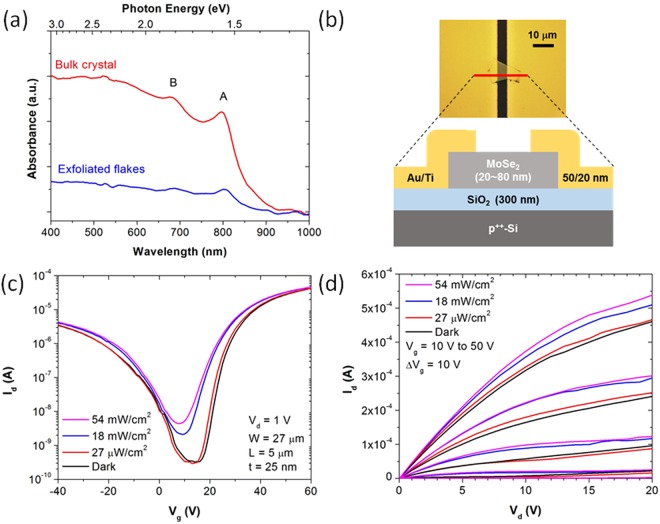
Before fabricating MoSe2 transistors, we first measure the optical absorbance of MoSe2 crystals and mechanically exfoliated flakes on sapphire substrates across visible and near-infrared spectral ranges (Fig. 1(a)). The MoSe2 crystal is thicker than 100 μm and the thickness of exfoliated MoSe2 flakes are in the range of 20–80 nm. Both samples show two excitonic absorbance peaks A and B at 1.55 eV and 1.82 eV, respectively, which is consistent with literature20. Next, multilayer MoSe2 transistors are fabricated on SiO2/Si substrates. Figure 1(b) shows the optical microscopy image of a completed MoSe2 transistor along with its schematic cross-section. The measured transfer curve of an MoSe2 transistor in Fig. 1(c) shows asymmetric ambipolar behavior with strong n-type characteristic (MoSe2 thickness (t) = 25 nm). For electron transport without light, the MoSe2 transistor exhibits on/off-current ratio (Ion/Ioff) of 105 and field-effect mobility (μFE) of 50.6 cm2V−1s−1 extracted from μFE = L(dId/dVg)/(WCoxVd), where L is the channel length (5 μm), Id is drain current, Vg is gate voltage, W is the channel width (27 μm), Cox is the oxide capacitance, and Vd is the drain voltage (1 V). For hole transport without light, Ion/Ioff of 104 and μFE of 2.8 cm2V−1s−1 are obtained. The n-type-dominant ambipolar behavior of MoSe2 transistors with Ti/Au electrodes was also observed in literature21,22. The output curves in Fig. 1(d) show linear region at low Vd suggesting decent contact properties. The transfer and output characteristics of an MoSe2 transistor in Fig. 1(c,d) show the increase of Id with the power density of incident light.
Figure 1.
(a) Absorbance spectra of MoSe2 crystals and mechanically exfoliated flakes on sapphire with two excitonic peaks A and B, (b) optical microscopy image and schematic cross-section of an MoSe2 phototransistor along the red line, (c) Id − Vg and (d) Id − Vd characteristics of an MoSe2 phototransistor with different optical power of incident light.
The photocurrent (Iph) of phototransistors based on transition metal dichalcogenides such as MoSe2 is known to be dominated by photoconductive effect and photogating effect23. In photoconductive effect, photogenerated excess carriers increase conductivity resulting in increased current. The photocurrent component flowing between two electrodes by photoconductive effect is given by24 , where Δσ, E, D, Δn, q, μ, η, Pin, h, ν, and τ are change in conductivity, electric field, depth of absorption region, change in carrier concentration, unit charge, carrier mobility, quantum efficiency, incident optical power, Planck constant, frequency of incident light, and carrier lifetime, respectively. The photoconductive component of Iph is proportional to areal power density of incident light Pin and weakly depends on Vg23,24. In photogating effect, one type of photogenerated carriers (electrons or holes) is trapped in localized states and the other type of carriers flows in the channel unrecombined. As this is equivalent to doping by the other type of carriers, photogating effect accompanies a shift of threshold voltage (Vth)25. As Vth shifts, the drain current changes from Id to Id + ΔId and it follows that26 , where gm, k, T, λ, Idark, and c are transconductance, Boltzmann constant, temperature, wavelength of incident light, dark current, speed of light, respectively. Thus, the photogating component of Iph shows logarithmic dependence on Pin and is roughly proportional to transconductance (gm)23,26.
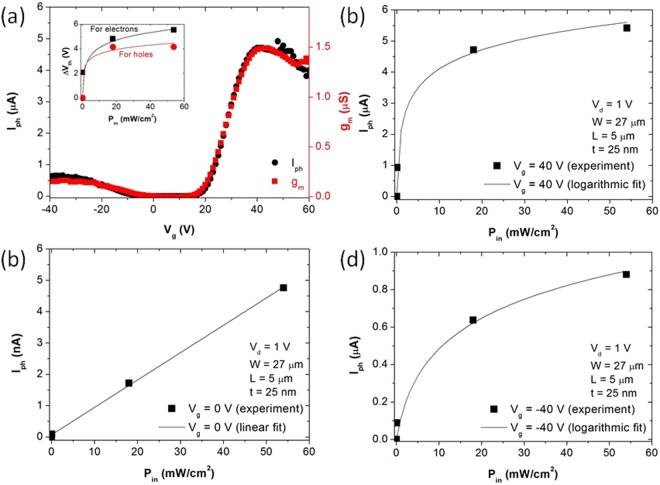
Figure 2(a) shows Iph and gm as a function of Vg for the same device in Fig. 1(c). The calculation of Iph (Iph = Ilight – Idark, where Ilight is Id in a detector with light), and gm (gm = dId/dVg) is based on the data in Fig. 1(c) at Pin = 18 mWcm−2. The similarity between Iph and gm suggests that photogating effect dominates the photoresponse of MoSe2 transistors. In the inset of Fig. 2(a), the change in Vth (ΔVth) for electrons and holes is shown as a function of Pin. The increasing change of Vth with increasing Pin also suggests the domiant role of photogating effect in our MoSe2 phototransistors. However, the dependence of Iph on Vg in Fig. 2(b) through (d) suggests that each effect dominates Iph at different range of Vg. Figure 2(b) through (d) show Iph of our MoSe2 phototransistor in an on-state for electrons (at Vg = 40 V), an off-state (at Vg = 0 V), and an on-state for holes (at Vg = −40 V) as a function of Pin in sequence. Iph is calculated based on the data in Fig. 1(c). The Iph in an on-state for electrons (at Vg = 40 V) and for holes (at Vg = −40 V) shows logarithmic dependence on Pin suggesting the dominant role of photogating effect. However, the linear dependence of Iph in an off-state suggests the dominant role of photoconductive effect. Such a distinct dependence of Iph on Vg regime was also observed in phototransistors based on MoS210, MoTe227, compound semiconductors26, and organic semiconductors28.
Figure 2.
(a) Iph and gm as a function of Vg; inset shows ΔVth for electrons and holes as a function of Pin (solid lines: logarithmic fit); Iph as a function of Pin (b) at Vg = 40 V, (c) at Vg = 0 V, and (d) at Vg = −40 V.
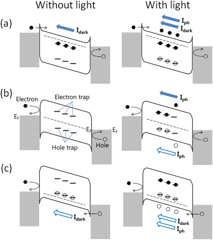
The observed dependence of Iph on Vg can be understood by the simplified energy band diagrams of an MoSe2 phototransistor under a bias (Vd) at different Vg in Fig. 3. For mechanically exfoliated MoS2 flakes and chemical vapor deposited MoS2 films, the existence of trap state was reported in literature13,29,30 as a result of structural defects at the surface and inside MoS2. Similarly, we assume that electron traps and hole traps exist in the energy bandgap of MoSe2 by structural defects at the surface and inside MoSe2. In Fig. 3(a) (at Vg = 40 V), the Fermi level (EF) is located close to the conduction band edge and the majority of electron traps are filled. Without light, Idark flows by the thermionic emission or tunneling of electrons. With light, the photogenerated holes fill hole traps and additional current Iph flows by the unrecombined photogenerated electrons. In Fig. 3(b) (at Vg = 0 V), EF moves toward midgap and the majority of electron traps and hole traps become unfilled. Without light, Idark is negligible as the high barrier height at the contact allows negligible injection of electrons and holes. With light, Iph is less than that in Fig. 3(a) as the photogenerated electrons and holes recombine or fill the trap states. In Fig. 3(c) (at Vg = −40 V), EF is close to the valence band edge and the majority of hole traps are filled. Without light, Idark flows by the thermionic emission or tunneling of holes. With light, the photogenerated electrons fill electron traps and additional current Iph flows by the unrecombined photogenerated holes.
Figure 3.
Schematic energy band diagrams of MoSe2 phototransistors with and without light (a) at Vg = 40 V, (b) at Vg = 0 V, and (c) at Vg = −40 V under an applied bias (Vd).
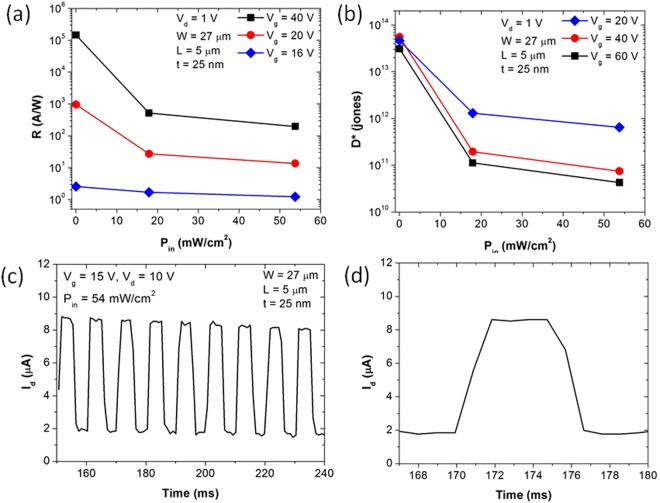
The performance of an MoSe2 transistor as a photodetector can be evaluated by responsivity (a measure of the electrical response to light) and specific detectivity (a measure of detector sensitivity)31. Responsivity (R) is given by R = (Ilight − Idark)/(PinA), where A is the area of the detector. Under the assumption that shot noise from Idark is the major contributor to the total noise, specific detectivity (D*) is given by32 D* = RA1/2/(2qIdark)1/2. Figure 4(a,b) show the calculated R and D* of the MoSe2 phototransistor at different Pin and Vg. Maximum R of 1.4 × 10⁵ AW−1 and D* of 5.5 × 10¹³ jones are obtained at Pin = 27 μWcm−2 and Vg = 40 V. These are the highest values of R and D* among MoSe2 phototransistors reported in literature so far (R = 0.01–238 AW−1 and D* = 1.0 × 10¹¹–7.6 × 10¹¹ jones at Pin = 10–100 mWcm−2)13,15–19. As R and D* increase with decreasing Pin, the enhancement of R and D* in this work may be due to the low Pin compared to that in literature. However, even at comparable Pin in the range of 18–54 mWcm−2, the maximum R and D* in this work (R = 519 AW−1 and D* = 1.3 × 10¹² jones) are about twice as high as those in literature. In Fig. 4(a,b), the overall dependence of R and D* on Pin and Vg is consistent with literature13. R increases as Pin decreases or Vg increases, while D* increases as Pin or Vg decreases. As Pin increases, more holes fill shallow trap states where lifetime is short. This results in faster recombination hence R decreases. When Pin increases, D* also decreases as R decreases and Idark remians unchanged. When Vg increases, electrical doping at higher Vg reduces contact resistance resulting in higher photocurrent and R. However, as Vg increases, Idark also increases, which degrades D*.
Figure 4.
(a) R and (b) D* as a function of Pin at different Vg; (c) Id as a function of time and (d) zoomed-in region in (c).
It needs to be mentioned that our MoSe2 transistors show wide device-to-device variation of μFE, R, and D* (Table S1 in Supplementary Information). Such wide device-to-device variation is commonly observed in the transistors based on transition metal dichalcogenides such as MoSe2 presumably because of the variation of intrinsic defects in crystals33. While it is very difficult to pinpoint the origin of high performance in the best device, the correlation between R and μFE in this work (Fig. S1 in Supplementary Information) suggests that the enhanced optoelectronic properties may be related to the enhanced electrical performance of our MoSe2 device. It is also supported by the fact that our MoSe2 device shows the highest mobility among MoSe2 transistors in Table 1.
Table 1.
Performance of MoSe2 phototransistors measured at Pin = 10–100 mWcm−2.
| Type of MoSe2 | μFΕ (cm2v−1s−1) | R (AW−1) | D* (jones) | Response time (ms) | Reference |
|---|---|---|---|---|---|
| Multilayer flake (Exfoliation) | 50.6 | 519.2 | 1.3 × 10¹² | 1.7 (rise) 2.2 (fall) | This work |
| Few layer flake (Exfoliation) | 19.7 | 97.1 | — | 15 (rise) 30 (fall) | 15 |
| Single layer film (CVD)i | — | 0.013 | — | 60 (rise) 60 (fall) | 16 |
| Multilayer flake (CVD)i | 10.1 | 93.7 | — | 400 (rise) 200 (fall) | 17 |
| Multilayer flake (Exfoliation) | 5.9 or 16ii | 0.1 or 16ii | 1.0 × 10¹¹ii | 5 (fall)ii | 13 |
| Few layer flake (Exfoliation) | 1.8 | 0.026 | — | 20 (rise) 20 (fall) | 18 |
| Few layer flake (Exfoliation) | 5.1 | 238 | 7.6 × 10¹¹ | — | 19 |
iChemical vapor deposition.
iiWith HfO2 encapsulation.
We also note the negligible correlation between the optoelectronic properties of MoSe2 devices and MoSe2 thickness. This may seem counterintuitive because the width of energy bandgap changes for thin MoS2 crystals (< ~4 nm in thickness)4 and light absorption depends on MoSe2 thickness. Yet, because the thickness of our MoSe2 flakes ranges from 20 nm to 80 nm, we expect negligible differences in energy bandgap in our MoSe2 devices. On the other hand, we expect higher responsivity for devices with thicker MoSe2 as more light is absorbed in thicker MoSe2. However, the responsivity shows negligible correlation with thickness of MoSe2 flakes in this investigation (Fig. S2 in Supplementary Information). This may be due to the variation of intrinsic materials quality overshadowing the effect of thickness. The mobility and detectivity in Fig. S2 also show negligible correlation with the thickness of MoSe2 flakes, supporting this argument.
To explore the response time of our MoSe2 phototransistors, we measure the time-resolved photoresponse of our MoSe2 phototransistors for multiple illumination cycles. Figure 4(c) shows the result for the same device in Fig. 1(c). The incident laser with a power density of 54 mWcm−2 is modulated with a square wave at 100 Hz at Vg = 15 V and Vd = 10 V. The nearly identical response for multiple cycles suggests the overall rebustness and reproducibility of our MoSe2 phototransistors. From a zoomed-in region in Fig. 4(d), we obtain rise time of 1.7 ms and fall time of 2.2 ms. (Rise time is calculated as the time taken by current to increase from 10% to 90% of the maximum current. Fall time is calculated as the time taken by current to decrease from 90% to 10% of the maximum current.) This is the fastest response time of MoSe2 phototransistors ever reported in literature, which ranges from 5 ms to 400 ms13,15–19. It is intriguing that our MoSe2 phototransistors exhibit high responsivity and fast response time. Because the long lifetime of carriers in photogating effect suggests slow response to light, the fast response time in our MoSe2 device may be related to the characteristics of trap states. One possibility is that trap states in our MoSe2 device may have shorter lifetime and higher density than those in literature. Then, while the shorter lifetime of trap states could provide fast response, the higher density of trap states could provide higher doping enhancing responsivity. However, we may only speculate at this stage and further investigation is needed on the characteristics of trap states including the distribution of trap energy, trap density, trap lifetime, and carrier capture probability.
Table 1 compares μFE, R, D*, and response time of MoSe2 phototransistors in literature. Because the measurement conditions, such as Vg, Vd, Pin, and excitation energy, can influence the device performance, comparable measurement conditions with those in literature are used in this work. Our MoSe2 phototransistors exhibit the best performance in terms of μFE, R, D*, and response time, demonstrating the feasibility of achieving high responsivity and fast response time in multilayer MoSe2 phototransistors. Future work combining controlled growth of materials with optimized device architecture and processing will further enhance the performance of MoSe2 phototransistors.
Conclusions
We report high-responsivity multilayer MoSe2 phototransistors with fast response time fabricated with mechanically-exfoliated MoSe2 flakes on SiO2/Si substrates. Our MoSe2 phototransistors exhibit asymmetric ambipolar behavior with strong n-type characteristic. Without light, high on/off-current ratio of 105 and field-effect mobility of 50.6 cm2V−1s−1 are obtained for electrons. Under 650-nm-laser, our MoSe2 phototransistor exhibits the best performance among MoSe2 phototransistors in literature including high responsivity (1.4 × 10⁵ AW−1), high specific detectivity (5.5 × 10¹³ jones), fast rise time (1.7 ms) and fast fall time (2.2 ms). The dependence of photocurrent on gate voltage and optical power density suggest that photocurrent is dominated by photogating effect in on-state and by photoconductive effect in off-state. These results demonstrate the feasibility of achieving high-performance multilayer MoSe2 phototransistors, providing potentially important implications on using MoSe2 phototransistors for a variety of applications including touch sensor panels, image sensors, solar cells, and communication devices.
Methods
Device fabrication
Multilayer MoSe2 flakes were obtained by gold-mediated mechanical exfoliation34 from bulk MoSe2 crystals (2D Semiconductors) and transferred to highly doped p-type Si wafer with thermally grown SiO2 (300 nm). The thickness of MoSe2 flakes measured by atomic force microscope (AFM, Park Systems XE-100) existed between 20 nm and 80 nm. To form source and drain electrodes (100 μm × 100 μm) on top of MoSe2 flakes, Ti (20 nm) and Au (50 nm) deposited by electron-beam evaporation were patterned using photolithography and etching. The device was then annealed at 200 °C in a vacuum tube furnace for 2 hours (100 sccm Ar and 10 sccm H2) to remove resist residue and to decrease contact resistance.
Device characterization
Optical absorbance of MoSe2 was measured by UV-visible spectroscopy (Perkin-Elmer Lambda 35). Electrical characterizations were carried out with current-voltage (I-V) measurements (Agilent 4155 C Semiconductor Parameter Analyzer) at room temperature. The photoresponse of MoSe2 phototransistors was measured with a 650-nm-laser (beam size of 3 mm) at different power densities (0.027, 18 and 54 mW cm−2). Dynamic on/off switching was conducted using a function generator (Tekronix AFG310).
Electronic supplementary material
Acknowledgements
This work was supported by the National Research Foundation of Korea (Grant NRF-2013K1A4A3055679 and NRF-2016R1A2B4014369) and Industrial Strategic Technology Development Program (Grant 10045145).
Author Contributions
H.L. and W.C. designed the experiments. H.L. fabricated the devices. H.L., J.A., S.I. and J.K. characterized the devices. H.L. and W.C. wrote the manuscript. All authors reviewed the manuscript.
Competing Interests
The authors declare no competing interests.
Footnotes
Electronic supplementary material
Supplementary information accompanies this paper at 10.1038/s41598-018-29942-1.
Publisher's note: Springer Nature remains neutral with regard to jurisdictional claims in published maps and institutional affiliations.
References
- 1.Wang QH, et al. Electronics and optoelectronics of two-dimensional transition metal dichalcogenides. Nat. Nanotechnol. 2012;7:699–712. doi: 10.1038/nnano.2012.193. [DOI] [PubMed] [Google Scholar]
- 2.Chhowalla M, et al. The chemistry of two-dimensional layered transition metal dichalcogenide nanosheets. Nat. Chem. 2013;5:263–275. doi: 10.1038/nchem.1589. [DOI] [PubMed] [Google Scholar]
- 3.Splendiani A, et al. Emerging Photoluminescence in Monolayer MoS2. Nano Lett. 2010;10:1271–1275. doi: 10.1021/nl903868w. [DOI] [PubMed] [Google Scholar]
- 4.Mak KF, et al. Atomically Thin MoS2: A New Direct-Gap Semiconductor. Phys. Rev. Lett. 2010;105:136805. doi: 10.1103/PhysRevLett.105.136805. [DOI] [PubMed] [Google Scholar]
- 5.Radisavljevic B, et al. Single-layer MoS2 transistors. Nat. Nanotechnol. 2011;6:147–150. doi: 10.1038/nnano.2010.279. [DOI] [PubMed] [Google Scholar]
- 6.Kim S, et al. High-mobility and low-power thin-film transistors based on multilayer MoS2 crystals. Nat. Commun. 2012;3:1011. doi: 10.1038/ncomms2018. [DOI] [PubMed] [Google Scholar]
- 7.Yin Z, et al. Single-Layer MoS2 Phototransistors. ACS Nano. 2012;6:74–80. doi: 10.1021/nn2024557. [DOI] [PubMed] [Google Scholar]
- 8.Choi W, et al. High-Detectivity Multilayer MoS2 Phototransistors with Spectral Response from Ultraviolet to Infrared. Adv. Mater. 2012;24:5832–5836. doi: 10.1002/adma.201201909. [DOI] [PubMed] [Google Scholar]
- 9.Lopez-Sanchez O. Ultrasensitive photodetectors based on monolayer MoS2. Nat. Nanotech. 2013;8:497–501. doi: 10.1038/nnano.2013.100. [DOI] [PubMed] [Google Scholar]
- 10.Zhang W, et al. High-Gain Phototransistors Based on a CVD MoS2 Monolayer. Adv. Mater. 2013;25:3456–3461. doi: 10.1002/adma.201301244. [DOI] [PubMed] [Google Scholar]
- 11.Kufer D, et al. Hybrid 2D–0D MoS2–PbS Quantum Dot Photodetectors. Adv. Mater. 2015;27:176–180. doi: 10.1002/adma.201402471. [DOI] [PubMed] [Google Scholar]
- 12.Wang X, et al. Ultrasensitive and Broadband MoS2 Photodetector Driven by Ferroelectrics. Adv. Mater. 2015;27:6575–6581. doi: 10.1002/adma.201503340. [DOI] [PubMed] [Google Scholar]
- 13.Kufer D, Konstantatos G. Highly Sensitive, Encapsulated MoS2 Photodetector with Gate Controllable Gain and Speed. Nano Lett. 2015;15:7307–7313. doi: 10.1021/acs.nanolett.5b02559. [DOI] [PubMed] [Google Scholar]
- 14.Bernardi M, et al. Extraordinary Sunlight Absorption and One Nanometer Thick Photovoltaics Using Two-Dimensional Monolayer Materials. Nano Lett. 2013;13:3664–3670. doi: 10.1021/nl401544y. [DOI] [PubMed] [Google Scholar]
- 15.Abderrahmane A, et al. High photosensitivity few-layered MoSe2 back-gated field-effect phototransistors. Nanotechnology. 2014;25:365202. doi: 10.1088/0957-4484/25/36/365202. [DOI] [PubMed] [Google Scholar]
- 16.Xia J, et al. CVD synthesis of large-area, highly crystalline MoSe2 atomic layers on diverse substrates and application to photodetectors. Nanoscale. 2014;6:8949–8955. doi: 10.1039/C4NR02311K. [DOI] [PubMed] [Google Scholar]
- 17.Jung C, et al. Highly Crystalline CVD-grown Multilayer MoSe2 Thin Film Transistor for Fast Photodetector. Sci. Rep. 2015;5:15313. doi: 10.1038/srep15313. [DOI] [PMC free article] [PubMed] [Google Scholar]
- 18.Hang Y, et al. Photo-Electrical Properties of Trilayer MoSe2 Nanoflakes. Nano. 2016;11:1650082. doi: 10.1142/S179329201650082X. [DOI] [Google Scholar]
- 19.Ko PJ, et al. High-performance near-infrared photodetector based on nano-layered MoSe2. Semicond. Sci. Technol. 2017;32:065015. doi: 10.1088/1361-6641/aa6819. [DOI] [Google Scholar]
- 20.Li Y, et al. Measurement of the optical dielectric function of monolayer transition-metal dichalcogenides: MoS2, MoSe2, WS2, and WSe2. Phys. Rev. B. 2014;90:205422. doi: 10.1103/PhysRevB.90.205422. [DOI] [Google Scholar]
- 21.Chamlagain B, et al. Mobility Improvement and Temperature Dependence in MoSe2 Field-Effect Transistors on Parylene-C Substrate. ACS Nano. 2014;8:5079–5088. doi: 10.1021/nn501150r. [DOI] [PubMed] [Google Scholar]
- 22.Pradhan NR. Ambipolar Molybdenum Diselenide Field-Effect Transistors: Field-Effect and Hall Mobilities. ACS Nano. 2014;8:7923–7929. doi: 10.1021/nn501693d. [DOI] [PubMed] [Google Scholar]
- 23.Furchi MM, et al. Mechanisms of Photoconductivity in Atomically Thin MoS2. Nano Lett. 2014;14:6165–6170. doi: 10.1021/nl502339q. [DOI] [PubMed] [Google Scholar]
- 24.Sze, S. M. & Ng, K. K. Physics of Semiconductor Devices. 3rd ed. (Wiley, New York, 2007).
- 25.Buscema M, et al. Photocurrent generation with two-dimensional van der Waals semiconductors. Chem. Soc. Rev. 2015;44:3691–3718. doi: 10.1039/C5CS00106D. [DOI] [PubMed] [Google Scholar]
- 26.Takanashi Y, et al. Characteristics of InAlAs/InGaAs high-electron-mobility-transistors under 1.3 μm laser illumination. IEEE Electron Device Lett. 1998;19:472–474. doi: 10.1109/55.735750. [DOI] [Google Scholar]
- 27.Yin L, et al. Ultrahigh sensitive MoTe2 phototransistors driven by carrier tunneling. Appl. Phys. Lett. 2016;108:043503. doi: 10.1063/1.4941001. [DOI] [Google Scholar]
- 28.Saragi TPI, et al. Photovoltaic and photoconductivity effect in thin-film phototransistors based on a heterocyclic spiro-type molecule. J. Appl. Phys. 2007;102:046104. doi: 10.1063/1.2770828. [DOI] [Google Scholar]
- 29.Ghatak S, Ghosh A. Observation of trap-assisted space charge limited conductivity in short channel MoS2 transistor. Appl. Phys. Lett. 2013;103:122103. doi: 10.1063/1.4821185. [DOI] [Google Scholar]
- 30.Zhu W, et al. Electronic transport and device prospects of monolayer molybdenum disulphide grown by chemical vapour deposition. Nat. Commun. 2014;5:3087. doi: 10.1038/ncomms4087. [DOI] [PubMed] [Google Scholar]
- 31.Konstantatos G, Sargent EH. Nanostructured materials for photon detection. Nat. Nanotechnol. 2010;5:391–400. doi: 10.1038/nnano.2010.78. [DOI] [PubMed] [Google Scholar]
- 32.Jha, A. R. Infrared Technology. (Wiley, New York, 2000).
- 33.Schmidt H, et al. Electronic transport properties of transition metal dichalcogenide field-effect devices: surface and interface effects. Chem. Soc. Rev. 2015;44:7715–7736. doi: 10.1039/C5CS00275C. [DOI] [PubMed] [Google Scholar]
- 34.Desai SB, et al. Gold-Mediated Exfoliation of Ultralarge Optoelectronically-Perfect Monolayers. Adv. Mater. 2016;28:4053–4058. doi: 10.1002/adma.201506171. [DOI] [PubMed] [Google Scholar]
Associated Data
This section collects any data citations, data availability statements, or supplementary materials included in this article.


