

Abstract
Thallium bromide (TlBr) is a promising semiconductor detector material for positron emission tomography (PET) because it can offer very good energy resolution and 3-D segmentation capabilities, and it also provides detection efficiency surpassing that of commonly used scintillators. Energy, timing, and spatial resolution were measured for thin (<1 mm) TlBr detectors. The energy and timing resolution were measured simultaneously for the same planar 0.87 mm-thick TlBr device. An energy resolution of (6.4±1.3)% at 511 keV was achieved at −400 V bias voltage and at room temperature. A timing resolution of (27.8±4.1) ns FWHM was achieved for the same operating conditions when appropriate energy gating was applied. The intrinsic spatial resolution was measured to be 0.9 mm FWHM for a TlBr detector with metallic strip contacts of 0.5 mm pitch. As material properties improve, higher bias voltage should improve timing performance. A stack of thin detectors with finely segmented readout can create a modular detector with excellent energy and spatial resolution for PET applications.
1. Introduction
Semiconductor radiation detectors are interesting candidates for positron emission tomography (PET) due to their better energy resolution compared with state-of-the-art scintillator-based detectors, and their capability to construct 3-D detectors with excellent localization accuracy [Lecomte 2009]. Among semiconductor detector materials, the most commonly studied for PET applications are cadmium telluride (CdTe) and cadmium zinc telluride (CZT) [Abbaszadeh and Levin 2017, Cates et al. 2015, Ariño et al. 2013, Groll et al. 2016, Mitchell et al. 2008, Morimoto et al. 2011, Vaska et al. 2007].
The energy resolution reported in CdTe and CZT is as good as 1.2% at 511 keV [Ariño et al. 2013]. With this energy resolution, Compton scattered events are very effectively rejected and the scatter background can be significantly reduced. Coincidence timing resolution of a few nanoseconds has been achieved with such detectors [Ariño et al. 2013, Mitchell et al. 2008, Okada et al. 2002]. A timing resolution as good as 430 ps FWHM has been achieved by detecting the Cerenkov light generated in TlBr with a photodetector [Ariño-Estrada et al. 2018], which requires an optical readout, as opposed to the charge induction readout discussed in this work. Although the charge induction readout does not provide time-of-flight (TOF) capabilities, there are applications (e.g. preclinical, breast and brain imaging) where TOF information is not currently of significant benefit, and where the energy resolution and high segmentation of semiconductor detectors can provide benefits in terms of image quality. The importance of the limited timing resolution in semiconductor radiation detectors lies in the probability of registering random coincidences and multiple events as it will define the maximum counting rate at which the detector can operate.
Detection efficiency is an important drawback of CdTe and CZT detectors. The attenuation of CdTe and CZT for 511 keV photons is much lower than that of commonly used scintillation materials in PET such as lutetium (yttrium) oxyorthosilicate (L(Y)SO) or bismuth germanate (BGO), see Table 1. Thus, the majority of events either fall outside the energy window (reducing efficiency), or interact multiple times (degrading the potential for high spatial resolution). One option to compensate for the lower detection efficiency is to increase the amount of material in the scanner. However, this means more material volume and, very likely, more channels of readout electronics, which leads to a significant increase in the complexity. A better alternative to overcome these limitations is to use semiconductor materials with much higher stopping power.
Table 1.
Density, effective atomic number (Zeff), and detection efficiency properties of LSO, BGO, CdTe, CZT, and TlBr, data from [Cherry et al. 2012, Lewellen 2010, Owens 2016, Berger et al. 2010].
| LSO | BGO | CdTe | CZT* | TlBr | |
|---|---|---|---|---|---|
| Density [g/cc] | 7.4 | 7.13 | 5.85 | 5.78 | 7.56 |
| Zeff | 66 | 73 | 50 | 50 | 74 |
| Linear Attenuation Coefficient for 500 keV photons [cm−1] | 0.89 | 0.99 | 0.54 | 0.54 | 1.04 |
| Attenuation Length for 500 keV photons [cm] | 1.12 | 1.01 | 1.84 | 1.87 | 0.97 |
| # of photons (or e−h+ pairs) per MeV of gamma ray Energy | 2.4×l04 | 8.2×l03 | 2×l05 | 2×l05 | 1.5×10⁵ |
CZT values for Cd0.9Zn0.1Te
Thallium bromide (TlBr) is a semiconductor material with the potential to simultaneously reach the energy resolution performance of CdTe and CZT detectors and the detection efficiency of scintillation crystals. On the one hand, TlBr can be operated as a direct detector and has a similar number of electron-hole pairs (e-h) created per deposited MeV of energy to CdTe and CZT (see Table 1), which means it can provide a similar energy resolution. On the other hand, TlBr has a high detection efficiency for 511 keV gammas due to its high density and effective atomic number, Zeff. The attenuation length for 511 keV photons is 0.97 cm, slightly shorter than that of BGO, the scintillation crystal with highest detection efficiency among those commonly used for PET.
Although the understanding of TIBr material growth and fabrication as a radiation detector is not nearly as advanced as that of CdTe or CZT, several publications present energy and timing resolution measurements with different detector geometries that come close to those of CdTe and CZT [Hitomi, et al. 2013, Hitomi et al. 2014, Kim et al. 2009]. However, the detectors used in such measurements are typically optimized for either energy or timing resolution measurements only. They are not employed to simultaneously measure both energy and timing resolution. In order to achieve good energy resolution, thick single carrier collection devices (e.g. small pixel arrays or Frisch collar devices) are preferred to minimize trapping effects while having good efficiency. In contrast, thin detectors with parallel electrodes show the best timing properties. Thus to obtain a TlBr detector that provides both good energy and timing resolution performance is a challenge.
In order to be considered for implementation in PET, TlBr detectors must demonstrate the ability to achieve good performance in spatial, energy and timing simultaneously. This work presents performance measurements of energy and timing resolution with the same planar TlBr device and also reports on intrinsic spatial resolution measurements using a TlBr strip detector. Combined, this data points the way forward to developing PET detectors based on TlBr that simultaneously exhibit high energy and spatial resolution combined with acceptable timing resolution for non-TOF applications.
2. Experimental Setup
Two different setups were used: one to obtain the simultaneous timing and energy resolution measurements using a planar TlBr detector, and another to obtain the spatial resolution measurements using the strip detector. The detectors were manufactured by Radiation Monitoring Devices and the TlBr was grown by the traveling molten zone (TMZ) method, more details on the material growth can be found in another publication [A. Churilov et al. 2008].
2.1. Timing Resolution and Energy Resolution Acquisition System
The timing and energy acquisition system consisted of two detectors: a planar TlBr detector and a reference detector. The TlBr detector had 0.87 mm thickness with 3-mm diameter electrodes (Fig. 1). The reference detector was a 5 mm cubic LYSO crystal coupled to a photomultiplier tube (PMT) (Hamamatsu R13449–10). A holder kept the LYSO-PMT and TlBr detectors distances 7 cm and 5 cm from the radioactive source, respectively. The detector set-up was placed inside a metal enclosure that kept the system light-tight and provided electromagnetic shielding against noise as well as proper grounding.
Figure 1:
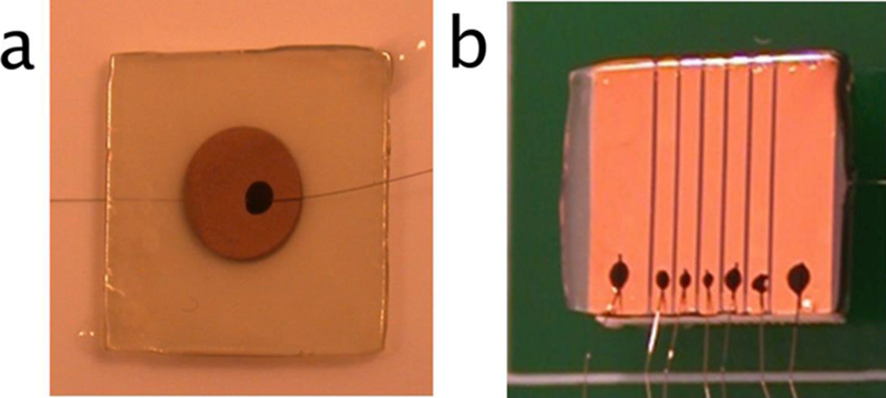
(a) TlBr detector with 0.87 mm thickness with 3-mm diameter electrodes made of Cr/Ti. Wires to read out signals are attached with a small amount of conductive carbon paste. (b) TlBr detector with dimensions of 5 mm × 5 mm × 0.74 mm mounted on a printed circuit board. The top electrode was made of Cr/Au and was segmented into 7 strips. The 5 central strips were 0.4 mm wide and with 0.1 mm interstrip distance while the 2 strips at the edges were ~1.2 mm wide. The opposite electrode was also made of Cr/Au and was not segmented.
The bias on the detector was increased slowly to its operating point of −400 V. The acquisition setup was maintained at 20° C during the data collection process. A 22Na encapsulated point-like source with an activity of 290 kBq (7.8 μCi) and an active area <0.5 mm was used.
Figure 2 depicts the electronics used in the readout of the coincidence acquisition system. The LYSO-PMT detector was connected to a constant fraction discriminator (CFD) to obtain the trigger signal. The trigger threshold was set above the noise level. The TlBr detector was coupled to a charge sensitive preamplifier (preamp) (Cremat CR-110) and later divided into two branches for separate energy and timing measurements. One of the branches was connected to a spectroscopy amplifier with 12 μs shaping time, the other one was connected to a time filter amplifier (TFA) (ORTEC 579) with 50 ns and 500 ns integration and differentiation time constants, respectively. The TFA output was connected to a CFD (ORTEC 935) to obtain the trigger signal. The trigger threshold was set right above the noise level to minimize the time walk. The trigger signals from both detectors were fed into an AND logic module (Philips Scientific 756) with a coincidence window of 2 μs, and its output was used as the trigger for the coincidence events. The trigger signal from the LYSO-PMT detector was connected to the start input of a time to amplitude converter (TAC) and the TlBr one was connected to the stop. As the TlBr is expected to be significantly slower than the reference detector, no real coincidence events are expected to happen when a TlBr signal is detected first.
Figure 2.

Schematic of the readout electronics for the coincidence acquisition system. The output signal of the TlBr was split. One branch was used to measure the energy and the other was used to obtain a trigger signal. A TAC was used to measure the detection time difference between the TlBr and the reference detector (LYSO-PMT). A desktop digitizer (CAEN 5740D) was used to digitize the output waveforms of the spectroscopy amplifier and the TAC.
A desktop digitizer (CAEN 5740D) was used to acquire the data. The output signals from the spectroscopy amplifier and the TAC were digitized at 62.5 MS/s and the total record length was 8000 samples. The TAC output was an almost-square signal with a narrow time width compared to the total record length. Its amplitude was measured by subtracting its offset to the maximum point of the waveform. The offset was evaluated by averaging the first 100 points of the waveform. The amplitude of the spectroscopy amplifier’s output was measured by subtracting the baseline to the maximum point of the waveform. The baseline was evaluated by averaging the region between the points 2000 and 4000 of the waveform, which were in the baseline range for the coincidence events. The waveform peak was approximately around the point 6000.
2.2. Spatial Resolution Measurement
The spatial resolution measurement system consisted of two detectors: a TlBr strip detector and a reference detector. The reference detector consisted of an LYSO crystal with dimensions 20×0.5×20 mm3 coupled to a Hamamatsu PMT (R13449–10). A holder was used to keep the radiation source and the LYSO-PMT detector aligned and separated ~12 cm to optimize the collimation process. The TlBr detector (Fig. 1B) was 5×5×0.74 mm3 with one of the electrodes segmented into 7 strips by using a wire mask when depositing the contacts on the TlBr material. The 5 central strips were 0.4 mm wide with 0.1 mm inter-strip distance. The 2 strips on the sides were 1.25 mm wide. The electrode on the opposing face was not segmented.
The TlBr strip detector was mounted on a printed circuit board (PCB) that processed the signal from each of the strips independently. The radiation source used was the same one used in the timing and energy resolution measurements. The holder was mounted on a motion stage with a position precision of 10 μm. The LYSO-PMT-source holder was moved in steps of 200 μm and the coincidence counting rate was measured for each position and strip. The TlBr detector was kept at ~3 cm from the radiation source for all the measurements. The curve of the count rate vs position for a strip was taken as the figure of merit to determine the spatial resolution of the device. The coincidence time window was 2 μs and the system was operated at room temperature. The readout electronics used were those of the coincidence system described in the previous subsection.
A series of 4 acquisitions of 5 min each was taken for each strip and position. The count rate was evaluated by averaging the total counts in the acquisitions and the standard deviation of each series was used as the measure of the uncertainty.
3. Results
3.1. Energy and Timing Resolution
The energy and timing resolution of a planar TlBr detector with 0.87 mm thickness at room temperature and biased at −400 V were measured. The energy spectrum from the TlBr detector is shown in Fig. 3. The pedestal was subtracted on an event-by-event basis during the acquisition process. The positions of the 511 keV photopeak, the Tl K-edge escape peak (~425 keV) and the Compton edge (340 keV), are approximately 1500, 1250, and 1100 digitizer units, respectively. These values show a linear behavior of the system for this range of energies.
Figure 3.
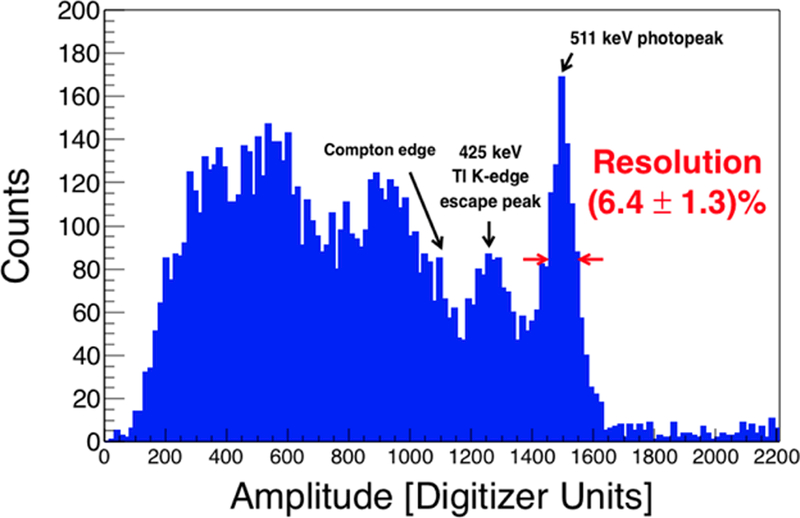
Energy spectra from 22Na with the 0.87 mm-thick TlBr detector biased at −400 V and at 20° C.
Linear interpolation was used to obtain the two x-axis values corresponding to the half-maxima on each side of the peak. The difference between these two values was taken as the FWHM. The distance between the interpolated value and the furthest of the two bin points used for the interpolation was taken as the uncertainty for the determination of the x-axis value for each half-maximum. The square root of the quadratic sum of the uncertainties for the two x-axis values was taken as the total uncertainty of the measurement. The energy resolution measured was (6.4±1.3)% at 511 keV.
Figure 4 shows a scatter plot of the coincidence detection time between the TlBr and the LYSO-PMT detectors vs the energy deposited in the TlBr detector. The FWHM and their associated uncertainties were evaluated as previously described. One can appreciate how the detection time distribution changes with the deposited energy in the TlBr detector. The detection time distribution was much more concentrated in the region of the 511 keV photopeak (1400–1700 digitizer counts) than in the low energy area (below 1200 digitizer counts), hence the detection time distribution has been studied as a function of the energy deposited in the TlBr detector.
Figure 4.
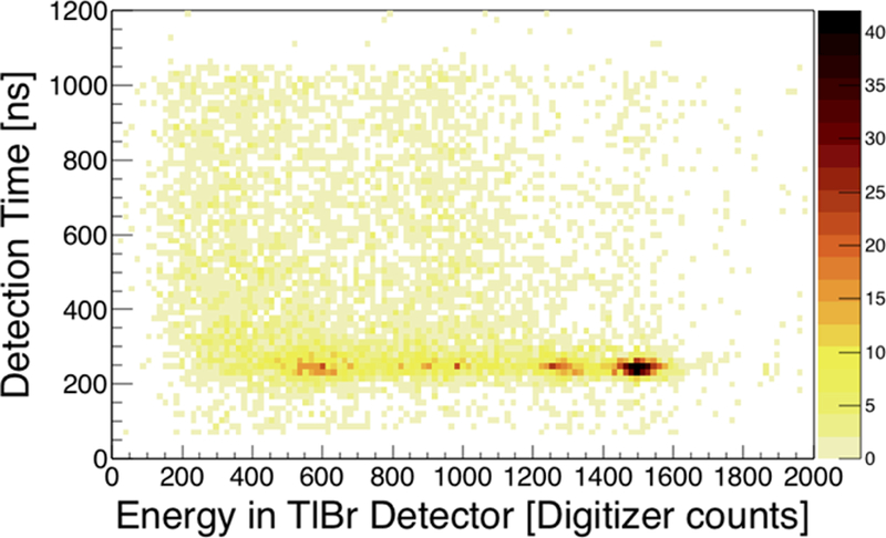
Detection time vs energy deposited in the TlBr detector. TlBr detector biased at −400 V and at room temperature.
The detection time distribution for coincidence events in different energy ranges are shown in Fig. 5. Three regions of interest have been defined: the full spectra, the range including the Τl K-edge escape peak and the 511 keV photopeak, and the range including the 511 keV photopeak only. The FWHM of the full distribution, (43.1±5.0) ns, improved to (37.1±4.9) ns and (27.8±4.1) ns after selecting only the events with amplitudes between 1200 and 1700 digitizer units (photopeak and escape peak), and 1400 and 1700 units (photopeak only), respectively. Using the most restrictive cut around the photopeak, the timing resolution was measured to be 27.8 ns.
Figure 5.

Detection time distribution for a 0.87mm thick TlBr detector biased at −400 V and kept at room temperature, operated in coincidence with a LYSO-PMT reference detector. Same dataset as in Fig. 4. (a) all events. (b) events with amplitudes between 1200 and 1700 counts (511 keV photopeak and escape peak). (c) events with amplitudes between 1400 and 1700 counts (511 keV photopeak only).
3.2. Spatial Resolution
Figure 6 shows the total counts acquired during the same collection time for four strips (S1–S4) in the TlBr strip detector and different positions of the source and thin reference detector (Fig. 6). The spatial distribution for each strip showed a very consistent behavior. The FWHM was evaluated for each curve by interpolation. All the measured curves had a FWHM of approximately 0.9 mm. Since the width of the gamma-rays incident on the detector is of order 0.5 mm (the width of the reference scintillator, and the TlBr and scintillator were approximately equidistant from the source; additionally the source has some small but finite size), the intrinsic spatial resolution is clearly demonstrated to be at the submillimeter level.
Figure 6.
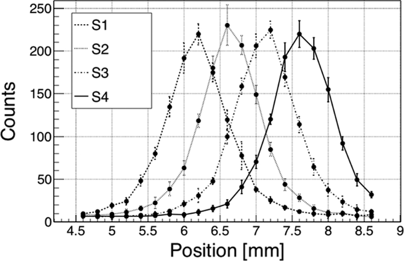
Number of counts in 5 min acquisitions for different relative positions of the source and reference detector with respect to the TlBr detector as the source and reference detector are stepped across 4 strips. The strips are 0.4 mm wide and are separated by a 0.1 mm gap. The counts were measured 4 times for each position and strip. The values in the plot are the average of the 4 measurements and the error bars are the standard deviations.
4. Discussion
A setup to operate TlBr detectors in coincidence with a reference detector was built. Measurements of the energy and timing resolution were simultaneously obtained for one planar detector. The spatial resolution of a similarly dimensioned TlBr detector with thin strip contacts was also measured.
The energy resolution measured for the 0.87 mm-thick planar TlBr detector, operated at −400 V and room temperature, was (6.4±1.3)% at 511 keV. For the same dataset, the coincidence time resolution was (43.1±5.0) ns for all energies, improving to (27.8±4.1) ns FWHM for events within the 511 keV photopeak. While a 6.4% energy resolution is better than most of the state-of-the-art scintillation crystal detectors for PET, the 28.7 ns FWHM is far from their subnanosecond timing performance. However, the possibility for improvement of this timing performance lies in obtaining materials with higher resistivity and therefore the ability to operate under higher electric field.
An intrinsic spatial resolution of 0.9 mm FWHM was achieved for a strip TlBr detector of thickness 0.74 mm with 0.4 mm wide strip contacts (0.5 mm pitch). This spatial resolution is promising for high-resolution PET applications, as by using narrow orthogonal strips on each side of thin detectors, and stacking detectors into a block, very efficient and high resolution 3D detectors can be built.
The manufacturing process for TlBr, as well as its operational characteristics, currently present challenges. The overall understanding of TlBr as a gamma-ray detector material is in a much earlier stage compared to CdTe or CZT. TlBr material properties are evolving: higher resistivity materials and a better understanding of metal contact behavior with the TlBr crystal should allow for operation under higher fields and prevent or minimize the effects of contact aging and degradation (Datta and Motakef 2015, Neslon et al. 2015).
Nevertheless, we have demonstrated the capability of manufacturing TlBr detectors with different configurations in terms of electrode shapes and geometries. We have also measured successfully, for the first time, simultaneous energy and coincidence timing resolution in the same TlBr detector. In our future work, we aim to fabricate detectors that can operate at higher electric fields (> 5 kV/cm) to improve the coincidence timing resolution while maintaining or improving the energy resolution performance in strip detectors.
Acknowledgments
This work was supported by the National Cancer Institute of the National Institutes of Health under award number R01 CA183994.
References
- Abbaszadeh S and Levin CS 2017. New-generation small animal positron emission tomography system for molecular imaging J. Med. Imaging 4 011008. [DOI] [PMC free article] [PubMed] [Google Scholar]
- Ariño G. et al. Energy and coincidence time resolution measurements of CdTe detectors for PET. J. Instrum. 2013:C02015. doi: 10.1088/1748-0221/8/02/C02015. [DOI] [PMC free article] [PubMed] [Google Scholar]
- Ariño-Estrada G, Mitchell GS, Kwon SI, Du J, Kim H, Cirignano LJ, Shah KS and Cherry SR 2018. Towards Time of Flight PET with a Semiconductor Detector Phys. Med. Biol 64 04LT01. [DOI] [PMC free article] [PubMed] [Google Scholar]
- Berger MJ, Hubbell JH, Seltzer SM, Chang J, Coursey JS, Sukumar R, Zucker DS and Olsen K 2010. XCOM: Photon Cross Section Database (version 1.5). [Online] Available: http://physics.nist.gov/xcom National Institute of Standards and Technology, Gaithersburg, MD [Google Scholar]
- Cates JW, Gu Y, Levin CS 2015. Direct conversion semiconductor detectors in positron emission tomography Mod. Phys. Lett. A 30 153001 [Google Scholar]
- Cherry SR, Sorenson JA and Phelps Μ E 2012. Physics in Nuclear Medicine 4th edn (Philadelphia: Saunders; ) [Google Scholar]
- Churilov AV, Higgins WM, Ciampi G, Kim H, Cirignano LJ, Olschner F and Shah KS 2008. Purification, crystal growth and detector performance of TlBr Proc. SPIE 7079, Hard X-Ray, Gamma-Ray, and Neutron Detector Physics X 70790K [Google Scholar]
- Datta A and Motakef S 2015. Cathode Degradation in Thallium Bromide Devices IEEE Trans. Nucl. Sci 62 1244–50 [Google Scholar]
- Groll A, Kim K, Bhatia H, Zhang JC, Wang JH, Shen ZM, Cai L, Dutta J, Li Q and Meng LJ 2016. Hybrid pixel-waveform (HPWF) enabled CdTe detectors for small animal gamma-ray imaging applications IEEE Tran. Rad. Plas. Med. Sci 1 3–14 [DOI] [PMC free article] [PubMed] [Google Scholar]
- Lecomte R 2009. Novel Detector Technology for Clinical PET Eur. J. of Nucl. Med. Mol. Imaging 36 Suppl 1:S69–85 [DOI] [PubMed] [Google Scholar]
- Lewellen TK 2010. The Challenge of Detector Designs for PET Nucl. Med. Mol. Imaging 195 301–309 [DOI] [PubMed] [Google Scholar]
- Hitomi K, Tada T, Onodera T, Shoji T, Kim SY, Xu Y and Ishii K 2013. Timing performance of TlBr detectors IEEE Trans. Nucl. Sci 60 2883–7 [Google Scholar]
- Hitomi K el al 2014. Characterization of Pixelated TlBr Detectors with Tl Electrodes Nucl. Instrum. Methods Phys. Res. A 747 7–12 [Google Scholar]
- Kim H, Cirignano L, Churilov A, Giampi G, Higgins W, Olschner F and Shah K 2009. Developing larger TlBr detectors – detector performance IEEE Trans. Nucl. Sci 56 819–23 [Google Scholar]
- Morimoto Y et al. 2011. Development of a 3D Brain PET Scanner Using CdTe Semiconductor Detectors and Its First Clinical Application. IEEE Trans. Nucl. Sci 58(5): 2181–9 [Google Scholar]
- Mitchell GS, Sinha S, Shekel JR, Bowen SL, Cirignano LJ, Dokhale P, Kim H, Shah KS and Cherry SR 2008. CdTe strip detector characterization for high resolution small animal PET IEEE Tran. Nuc. Sci 55 870–6 [Google Scholar]
- Nelson AJ, et al. 2015. Auger Compositional Depth Profiling of the Metal Contact-TlBr Interface Proc. SPIE 9595, Radiation Detectors: Systems and Applications XVI, 959507 (August 27, 2015) [Google Scholar]
- Okada Y, Takahashi T, Sato G, Watanabe S, Nakazawa K, Mori K and Makishima K 2002 CdTe and CZT detectors for timing measurements IEEE Trans. Nucl. Sci 4 1986–92 [Google Scholar]
- Owens A 2016. Compound semiconductor radiation detectors CRC Press Boca Raton, FL, USA [Google Scholar]
- Vaska P, et al. 2007. A Prototype CZT-based PET Scanner for High Resolution Mouse Brain Imaging IEEE Nucl. Sci. Symp. Conf. Rec. 2007 M19–171 [Google Scholar]