

Abstract
Three-dimensional (3D) printing now enables the fabrication of novel 3D structural electronics and microfluidics. However, conventional subtractive manufacturing processes for MEMS fabrication relatively limit device structure to two dimensions and require post-processing steps for interface with microfluidics. Thus, the objective of this work is to create an additive manufacturing approach for fabrication of 3D microfluidic-based MEMS devices that enables 3D configurations of electromechanical systems and simultaneous integration of microfluidics in a one-pot manufacturing process. Here, we demonstrate the ability to fabricate microfluidic-based 3D microelectromechanical systems (MEMS) that contain orthogonal out-of-plane piezoelectric sensors and actuators using additive manufacturing. The devices were fabricated using a microextrusion 3D printing system that contained integrated pick-and-place functionality. Additively assembled materials and components included 3D printed epoxy, polydimethylsiloxane (PDMS), silver nanoparticles, and eutectic Gallium-Indium as well as robotically embedded orthogonal out-of-plane piezoelectric chips (lead zirconate titanate (PZT)). Electrical impedance spectroscopy and finite element modeling studies showed the embedded PZT chips exhibited multiple resonant modes of varying mode shape over the 0 – 20 MHz frequency range. Flow visualization studies using neutrally buoyant particles (diameter = 0.8 – 70 μm) confirmed the 3D printed MEMS devices generate bulk acoustic waves (BAWs) capable of size-selective manipulation, trapping, and separation of suspended particles in droplets and microchannels. Flow visualization studies in continuous flow format showed suspended particles could be moved toward or away from the walls of microfluidic channels based on selective actuation of in-plane or out-of-plane PZT chips. This work suggests additive manufacturing potentially provides new opportunities for the design and fabrication of acoustofluidic and microfluidic devices.
Table of Contents Entry
Additive manufacturing enables the fabrication of 3D acoustofluidics with microfluidic channels interwoven among 3D acoustic transducer configurations.
1. Introduction
Additive manufacturing, also referred to as 3D printing, has emerged as a flexible multi-material processing technique and appears poised to enable the design and manufacture of novel functional materials and devices.1–6 In particular, the ability to 3D print multiple materials, notably polymers and functional nanomaterials, has led to the fabrication of novel electronic4, 6–9 and microfluidic devices.1, 5, 10 The current paradigm for 3D printing functional multi-material and -component systems, such as 3D electronics, is based on formulating all materials and components into printable matrices. For example, structural and functional materials can be formulated as printable suspensions, foams, gels, resins, and melts.2, 11, 12 However, in situ integration of non-printed components, such as microchips, remains an open challenge that currently limits the design space for 3D printed electronics. Thus, new approaches for robust integration of non-printed functional components with 3D printed architectures could expand our ability to create novel 3D printed electronics, and ultimately, functional multicomponent systems.13
Embedding of non-printed components within 3D printed architectures provides a means of enhancing the performance and functionality of 3D printed systems, and thus, has been leveraged toward the fabrication of novel electronic devices.14, 15 For example, 3D printed magnetic flux sensors,16 electrode-integrated microfluidic devices,17 circuits,7, 16 and nuclear spin polarizers18 have been produced by embedding non-printed electronic components in 3D printed architectures. Embedding techniques are classified by the mechanism for grasping and placement of non-printed components, such as in pick-and-place techniques.19 Although various pick-and-place techniques exist (e.g. manually or robotically guided20 adhesion, suction,21, 22 or mechanical23 mechanisms),24 robotic suction-based techniques are especially promising given tolerance for surface characteristics of the embedded component, ability to control grip force, and fast cycle time.19 To date, the most common embedded components have included conductive materials,25, 26 discrete circuit components,15, 27 and integrated circuits.27, 28 Given ceramic materials serve as functional components for a variety of electronic devices due to their electromechanical coupling properties, the ability to 3D print ceramic-based multicomponent systems would be desirable. However, although 3D printing appears to be an emerging technique for shaping ceramic materials,29 processing and post-processing requirements30 (e.g. the need for support materials, sintering, and poling, respectively) impede the integration of ceramics into 3D printed polymeric architechures.31 Consequently, the ability to construct 3D printed ceramic-based electronic devices remains an open challenge. Thus, the ability to interweave non-printed technical ceramics, such as piezoelectric materials, with 3D printed materials via embedding could potentially enable the fabrication of novel multicomponent electronic devices,13 such as microelectromechanical systems (MEMS).
Acoustofluidic devices are a versatile class of analytical platforms for small-volume static liquid and flow-based biosensing and bio-separation applications.32–34 Flexibility in biological and biomedical applications arises from the various methods for actuating surface and bulk acoustic waves via electroded piezoelectric materials (e.g. via interdigitated or parallel plate electrodes, respectively). To date, transmitted surface acoustic waves (SAWs) actuated by interdigitated electrodes have been applied in both static35–38 and flow formats32, 39 (e.g. droplet- or microfluidic-based, respectively). Although microfabrication approaches have enabled the creation of novel interdigitated electrode geometries for SAW-based acoustofluidic devices, the techniques for anchoring and embedding the piezoelectric components for bulk acoustic wave (BAW)-based acoustofluidic devices remain limited. Thus, the ability to embed piezoelectric chips in 3D printed architectures in situ during the 3D printing process could provide unique electroding, anchoring, and acoustic matching strategies, thereby generating new opportunities for the design and application of BAW-based acoustofluidic devices. Furthermore, the ability to 3D print acoustofluidic devices provides a potential pathway toward highly reconfigurable and integrated acoustofluidic platforms.39
Here, we highlight a novel approach for integrating piezoelectric materials with multi-material 3D printed microfluidic architectures using a pick-and-place microextrusion 3D printing process. Specifically, we demonstrate the utility of the electronic integration technique via the printing of 3D microfluidic-based MEMS devices composed of thermosetting polymers for structural anchoring, elastomers for acoustic impedance matching, functional nanomaterials for conductive pathways, and embedded lead zirconate titanate (PZT) chips for sensing and actuation purposes. Electrical impedance spectroscopy and finite element modeling studies show the printed devices exhibit multiple resonance modes and corresponding mode shapes over the 0 – 20 MHz frequency range. We also show via flow visualization studies that the acoustic trapping patterns and streaming profiles correlate with the embedded PZT chip mode shapes. The printed devices exhibit frequency- and particle size-dependent regimes of acoustic particle trapping and streaming, with a transition zone occurring at ~15 MHz and ~1 μm, respectively. This work shows 3D printing provides new opportunities for the design and fabrication of 3D MEMS, acoustofluidic, and microfluidic devices.
2. Materials and Methods
2.1. Materials
Glass cover slips (22 × 22 mm2) were purchased from AmScope. Epoxy (Hysol E-90FL) was from Loctite. Lead zirconate titanate sheets (PZT-5A; 127 μm thick) with nickel (Ni) electrodes were from Piezo Systems, Inc. (Woburn, MA). Sylgard 184 silicone (PDMS) was from Dow Corning. Polyethylene particles (70 and 25 μm) were from Cospheric (Santa Barbara, CA). Polybead particles (6 and 0.8 μm) were from Polysciences, Inc. (Warminster, PA). Fluorescent Fluoro-Max particles (26, 6, and 0.8 μm) were from ThermoFisher Scientific. Ultrapure de-ionized water (DIW) was from a commercially available DIW system (Direct-Q 3UV; Millipore). Poly (ethylene glycol) dimethacrylate (PEG-DA) (MW = 750 Da), silver nitrate, poly(acrylic acid) sodium salt (PAA) (MW = ~15 kDa, 35% in water), diethanolamine, ethylene glycol, ethanol (200 proof), and eutectic Gallium-Indium (EGaIn) were from Sigma Aldrich. Hydrochloric acid (HCl) was from Fisher Scientific.
2.2. Preparation of 3D Printed and Embedded Materials
PZT sheets were diced into 5 × 1 × 0.127 mm3 chips for use as the embedded piezoelectric component in the 3D printed acoustofluidic devices (American Dicing; Liverpool, NY). The 3D printed materials included an elastomer (PDMS), a thermosetting polymer (epoxy), and a suspension of conductive (silver; Ag) nanoparticles. PDMS was prepared as a 10:1 ratio by weight of the base to curing agent. Epoxy was prepared as a vendor-specified mixture of the two-part system. The Ag nanoparticle suspension was synthesized as previously described.40 Briefly, 40 g of diethanolamine and 3.6 g PAA were dissolved in 50 mL of DIW and stirred for 2 hours at room temperature. Separately, a solution of 20 g silver nitrate in 20 mL water was prepared. The silver nitrate solution was slowly added to the diethanolamine-PAA solution while stirring vigorously. The mixture was stirred gently for 24 hours until black. The resulting solution was then titrated with 120 mL ethanol to form a precipitate. The supernatant was decanted, and the Ag slurry was centrifuged at 5,000 rpm for 40 minutes (Storvall ST16; Thermo Scientific). The supernatant was again removed. Then a humectant solution (30 wt% ethylene glycol in water) was added to the nanoparticles at 10 wt% and homogenized. The resultant suspension was placed under light vacuum for 30 minutes prior to printing.
2.3. Fabrication of Acoustofluidic Devices via the Pick-and-Place 3D Printing Process
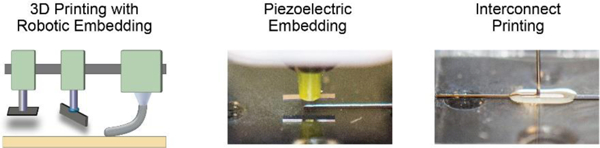
A custom pick-and-place microextrusion 3D printing system comprised of an industrial dispensing robot (F5200N; Fisnar; repeatability = 20 μm) and high precision digital dispensers (Ultimus V; Nordson EFD) was used for this work (see Figure S1 of Supporting Information). Tool paths were written using vendor-provided software (RoboEdit; Fisnar). Printing of the device began by placing a glass substrate on the heated print stage (T = 100°C) using the suction-based pick-and-place tool (16 gauge nozzle). Ag was then printed from the edge to the center of the substrate using a 33 gauge tip at 4 mm/s with an applied pressure of 10 – 15 psi. Subsequently, the pick-and-place tool was used to grasp a PZT chip from the edge of the build area and place it on the end of the Ag pathway located in the center of the substrate by applying a vacuum of 0.65 psi to grasp the chip and a pressure of 0.1 psi to release it, respectively. Epoxy was then printed around the chip using a 27 gauge tapered tip and a high pressure adapter (HP7x; Nordson) at 2 – 4 mm/s with a pressure of 30 – 40 psi. The stage was then heated to 100°C for 10 minutes using a Peltier to cure the epoxy. Next, Ag was printed from the top face of the PZT chip at the center of the device to the edge of the substrate extending in the opposite direction of the first Ag pathway. Subsequently, the printed device was heated for 10 minutes at 100°C to evaporate excess liquid from the printed Ag suspension. An epoxy boundary was then printed at the edges of the substrate located 1 mm inside the ends of printed conductive pathways and allowed to solidify for 10 minutes at 100°C. PDMS was then printed within the external epoxy boundary using a 20 gauge tip at 8 mm/s with an applied pressure of 4 psi, and the printed device was allowed to cure for two hours at 100°C. This process resulted in a device that contained a single in-plane transducer. Subsequently, a second pick-and-place operation was used to integrate a second out-of-plane transducer on the chip that was orthogonal to the previously embedded in-plane transducer by the following steps. First, a single filament of silicone was printed on the chip in the direction of the printed Ag conductors displaced by a distance of 3 mm from the center of the in-plane transducer using a 27 gauge tip at 1 mm/s to provide a medium with high adhesion for the subsequently embedded piezoelectric chip. Subsequently, a second piezoelectric chip was grasped from the long edge (i.e., thickness dimension) using a second pick-and-place tool based on an adhesive grasping mechanism (here, a silicone-filled 27 gauge tip) and inserted 200 μm into the silicone filament for placement. The pick-and-place tool was subsequently retracted leaving the piezoelectric chip placed in an out-of-plane configuration with the normal vector of the chip’s face orthogonal to that of the previously integrated chip. The silicone was then allowed to cure. An epoxy anchor was printed around the base of the piezoelectric chip covering the silicone filament and making mechanical contact with the chip and PDMS substrate on all sides leaving 0.5 mm of the piezoelectric chip exposed to air. This process resulted in a device that contained a 3D configuration of orthogonal acoustic transducers (i.e., one in-plane and one out-of-plane transducer).
A Y-shaped microfluidic channel was then printed in between the two transducers according to a previously reported technique.41 Briefly, two EGaIn filaments were printed in a Y-shape on the PDMS substrate directly in between the two orthogonal transducers using a 20 gauge tip with a pressure of 0.1 – 0.3 kPa and print speed of 1.7 – 2.2 mm/s. Following printing, the EGaIn filament and out-of-plane acoustic transducer were insulated by application of a second PDMS layer on the device. After PDMS curing, the EGaIn was removed from the microchannel by continuous flow of a 1M HCl solution down the channel. The channel was then rinsed with DIW and the inlet was connected with a syringe pump via external tubing.
2.4. Profilometry Studies
The height and cross-sectional profile of each 3D printed and embedded component in the printed construct was characterized using a profilometer (Form Talysurf S3F; Taylor Hobson) throughout the 3D printing process. All profiles were acquired at a scan speed of 0.5 mm/s using a 2 μm diamond conispherical stylus tip.
2.5. Electrical Impedance Spectroscopy
The electrical impedance responses of the 3D printed devices were measured using an impedance analyzer (E5061B; Keysight). The electrical impedance response at 100 mV AC with zero DC offset was recorded as phase angle (φ) and impedance (Z) versus frequency data over the 0 – 20 MHz frequency range.
2.6. Finite Element Analysis of Electromechanical Frequency Response and Modal Mechanics
Electromechanically-coupled eigenfrequency and frequency response simulations of the printed device were done as previously reported.42, 43 All studies were performed using commercially available finite element analysis (FEA) software (COMSOL Multiphysics, Version 5.2a). A frequency domain analysis was conducted in 3D using the piezoelectric device interface, which enables the coupling of a solid mechanics problem using the Structural Mechanics module with an electrostatics problem using the AC/DC module. The domain was generated using the graphics-user interface according to the dimensions of the embedded PZT chip (5 × 1 × 0.127 mm3). The material properties of PZT were selected from the software’s built-in library. Damping was modeled as an isotropic structure loss factor (η = 0.01).42 The mechanical boundary conditions included a fixed constraint condition on all chip faces except the top and bottom faces. No initial deformation, stress, or external forces were applied. The electrostatic boundary conditions included a zero-charge condition on all chip faces except the top and bottom faces. A 20 V electrical potential and a ground condition were applied on the top and bottom faces, respectively. The model was then discretized using a physics-controlled mesh. Subsequently, the mode shapes and electrical impedance spectrum were obtained over 0.1 – 20 MHz at a step size of 0.01 MHz using an eigenvalue solver. Proper density of the mesh was validated by examining the convergence of the maximum displacement (D), Z, and φ by iterating from an extremely coarse to an extra fine mesh element size. The total current (I) was calculated by integrating the boundary current density over the electrode area at each frequency value. Z and φ were then calculated as Z = V/I and φ = tan−1[Im(I)/Re(I)], respectively.
2.7. Sensing of Acoustic Waves
Acoustic waves generated by the electrically excited embedded PZT chip were sensed by integrating a secondary PZT chip with the elastomeric layer above the epoxy-embedded chip. The separation distance between the epoxy-embedded and secondary chips was ~1 mm. Sensing of acoustic waves was done by recording the voltage signal (Vs) generated in the secondary chip using an oscilloscope (DS1050E; Rigol) while the epoxy-embedded chip was excited at 20 Vp-p (Va). Voltage responses were acquired while the device was driven at each resonant mode. The fast Fourier transform (FFT) of the acquired voltage time series data was calculated using MATLAB. We note that the secondary PZT sensing chip was not present for subsequent acoustofluidic flow visualization studies (e.g. particle manipulation studies), but served to characterize the acoustic waves generated by the device.
2.8. Droplet- and Continuous Flow-based Particle Separation Studies
All polymer microparticle suspensions, including neutrally buoyant polyethylene (70 μm and 25 μm), Polybead (6 and 0.8 μm), and Fluoro-Max (26, 6, and 0.8 μm) particles, were prepared in DIW at a concentration of 1 mg/mL. For droplet-based particle separation studies, 3 μL of a given particle suspension was deposited on the top surface of the printed device 1 mm from the long side of the in-plane PZT chip (located in between the two orthogonal transducers) in the absence of vibration, thus forming a droplet that contained suspended particles. After allowing five seconds for the particle distribution to reach a stable initial condition, the in-plane transducer was then excited at 20 Vp-p at a fixed frequency. Micrographs and videos of particle trajectories throughout the stimulation period were acquired using a stereoscope (OM4413; Omano). Fluorescence micrographs were acquired using a fluorescence microscope (Axio Zoom.V16; Zeiss). For continuous flow-based particle separation studies, a particle suspension containing 6 μm polybead particles was first flowed through the 3D printed microfluidic channel at 25 μL/min in the absence of vibration, thus allowing a steady state flow profile to develop. The in-plane, out-of-plane, or both in- and out-of-plane transducers were then excited at 20 Vp-p at a fixed frequency. Micrographs of the flow profile throughout the stimulation period were acquired using a stereoscope (OM4413; Omano).
2.9. Image Analysis of Particle Distributions
Light and fluorescence micrographs were analyzed in ImageJ to quantify the particle distributions for the droplet-based particle separation studies. Micrographs were first imported into ImageJ and grey scaled. Subsequently, the grey scale intensity across the diameter of the droplet was plotted. Intensity profiles were then normalized by the maximum grey scale value.
3. Results and Discussion
3.1. 3D Printing of Acoustofluidic Devices via Robotic Embedding of Piezoelectric Components
Although 3D printed electronics widely vary regarding design, function, and utility, the incorporation of electromechanically coupled materials remains an open challenge due to limitations associated with ceramic integration. As a result, manufacturing processes that enable the assembly of ceramics, polymers, and nanomaterials could potentially provide a novel fabrication approach for ceramic-based electronics, such as MEMS. As shown schematically in Figure 1, a multi-material pick-and-place 3D printing process could potentially enable the in situ integration of electroded technical ceramics, such as piezoelectric materials, into 3D printed polymer architectures, thus providing a novel pathway toward creating novel MEMS, such as acoustofluidic devices. We next examined the ability to 3D print acoustofluidic devices based on robotically embedded PZT chips, given they serve as actuators for a variety of MEMS, including dynamic-mode biosensors and acoustofluidic devices.44–46 As shown in Figure 2a, the multi-step printing process involved: 1) pick-and-place of a glass substrate (22 × 22 mm2; 227 mg); 2) 3D printing of a conductive Ag pathway on the substrate; 3) pick-and-place of the PZT chip (5 × 1 mm2; 2.5 mg) on the conductive pathway with an in-plane configuration, thereby bonding the printed Ag pathway to the PZT Ni electrode; 4) 3D printing of an epoxy anchor; 5) 3D printing of a conductive Ag pathway from the top of the chip onto the substrate, thereby forming a symmetrically electroded PZT chip; 6) 3D printing of an epoxy support wall; and 7) 3D printing of a PDMS insulation layer. As shown in Step 3 of Figure 2a, the robotically guided suction-based pick-and-place tool enabled placement of the chip on the printed Ag pathway with high precision. As shown by comparison of Steps 3 and 4 in Figure 2a, the release pressure associated with chip placement did not change the chip’s position relative to the release location. In addition, the shear stress exerted by the 3D printed epoxy anchor on the PZT chip during printing did not change the position of the PZT chip relative to the placement location (see Steps 3 and 4). Given the printed and embedded materials exhibit differences in thickness, the device exhibits a non-uniform height profile throughout the printing process. For example, the profilometry data in Step 3 show that embedding of the in-plane PZT chip causes a 143 μm height difference between the substrate and the top of the embedded PZT chip, which requires the subsequent printing of a 3D conductive Ag pathway to the chip’s top electrode. As shown in Step 4, the height profile of the printed epoxy was conducive for printing a 3D conductive Ag pathway (17 μm high and 750 μm wide) that extended from the top electrode of the PZT chip to the substrate (see Figure S2 of Supporting Information for a magnified view of the profilometry data). Ultimately, as shown in Figure 2b, the printing process resulted in a 729 μm thick, five-layer device composed of an embedded and electroded PZT chip within a matrix of 3D printed polymers and functional nanomaterials. A video of the printing process is shown in Video S1 of Supporting Information.
Fig 1.
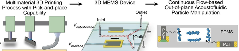
Additive manufacturing concept for fabrication of 3D microfluidic MEMS devices. A combination of 3D printing and robotic embedding facilitates the integration of orthogonal in-plane and out-of-plane piezoelectric transducers, functional 3D printable materials, and microfluidic channels. In-plane and out-of-plane piezoelectric transducers facilitate the trapping of continuously flowing particles in microfluidic channels in transverse and lateral directions.
Fig. 2.
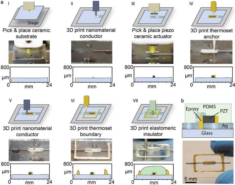
a) Highlight of the seven fabrication steps (I-VII) for the 3D printed acoustofluidic device including 3D printing and embedding processes. Each step shows in vertically descending order: the assembly schematic, a photograph of the device during the fabrication step, and the height profile of the device after completion of the step. b) Cross-sectional schematic (top) and photograph (bottom) of the device.
3.2. Frequency Response and Modal Mechanics of the 3D Printed Acoustofluidic Devices
As a dynamic electromechanical component, the embedded PZT chip exhibits various natural modes of vibration (i.e. resonant modes). Thus, we next examined the electrical impedance response of the in-plane PZT transducer over the 0 – 20 MHz frequency range. As shown in Figure 3a, the in-plane transducer exhibited various resonant modes as identified by peaks or inflection points in phase angle and impedance data, respectively. For example, the in-plane transducer exhibited four distinct resonant modes at 1.9 ± 0.1, 4.7 ± 0.1, 7.4 ± 0.1 and 17.2 ± 0.6 MHz (n = 13 devices). The observed coupling of mechanical motion to impedance change in the PZT layer is consistent with millimeter-scale piezoelectric sensors and actuators.42, 43 Having identified the frequencies of the in-plane transducer’s multiple resonant modes via electrical impedance measurements, we next conducted finite element simulations to examine the modal mechanics associated with each resonant mode. Given the PZT was embedded in a printed epoxy anchor (see Figure 3b), the transducer was modeled as an externally clamped vibrating structure. As shown by the first panel of Figure 3a, the simulated electrical impedance response of the in-plane transducer exhibited resonant modes with high impedance-coupling at 1.6, 4.8, 7.6, and 17.3 MHz, which agreed reasonably to the experimentally measured values. Figure 3c shows the 3D mode shape at each resonant frequency in terms of the transverse (out-of-plane) displacement (D(z)) (see Figure S3 of Supporting Information for corresponding displacement profiles in the width direction). As shown by the 3D mode shapes and corresponding displacement profiles in Figure 3c, the in-plane transducer exhibited transverse modes at 1.9 and 4.7 MHz and combination modes at 7.4 and 17.2 MHz with maximum transverse displacements (D(z)max) of ~18, 14, 12, and 3 nm, respectively.
Fig. 3.
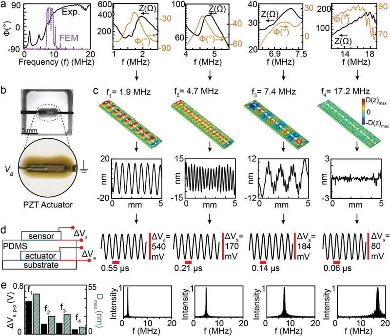
a) Experimentally measured and simulated electrical impedance response of the 3D printed acoustofluidic devices over 0 – 20 MHz and highlight of experimentally measured impedance (Z) and phase angle (φ) characteristics from four resonant modes that exhibit strong impedance-coupling. b) Photograph of the embedded PZT chip highlighting the acoustic source. c) Calculated 3D mode shape and displacement profile (dashed line) for each of the resonant modes shown in terms of the transverse displacement. d) Secondary transducer configuration for sensing of acoustic waves generated by the embedded PZT chip showing the corresponding voltage signal generated in the secondary transducer (Vs,p-p) at each mode. e) Comparison of the voltage generated in the secondary acoustic transducer with the maximum total displacement (Dmax) calculated using finite element simulations for each resonant frequency (fn). Also shown is the fast Fourier transform of the measured voltage signal shown in (d).
3.3. Sensing of Acoustic Radiation
Having shown that the in-plane transducers exhibit various resonant modes of different mode shape and displacement magnitude, we next examined the ability to sense acoustic waves generated by the transducer through embedding of a secondary piezoelectric transducer. As shown schematically in Figure 3d, excitation of the in-plane transducer with voltage (Va) produces an acoustic wave that can be measured in terms of a generated voltage (Vs) in a secondary piezoelectric transducer. Figure 3d shows the measured voltage generated in the secondary piezoelectric transducer for each of the four modes in the presence of device excitation at Va = 20 V. As shown in Figure 3e, the magnitude of the generated voltage in the secondary piezoelectric transducer correlated with the calculated maximum total displacement (Dmax) for each mode. For example, the generated voltage was 540, 170, 184, and 80 mV at 1.9, 4.7, 7.4, and 17.2 MHz, respectively, and Dmax was 45, 20, 22, and 8 nm, respectively. As shown in Figure 3e, we also verified that the frequency of the generated voltage matched the excitation frequency. Ultimately, the data in Figure 3 show the in-plane transducer exhibits various resonant modes and generate acoustic waves that propagate through the top printed PDMS layer. Thus, the coupling of fluid systems, such as a droplets or microfluidic streams, with the 3D printed MEMS device could enable novel MEMS architectures.
3.4. Droplet-based Acoustofluidic Particle Manipulation Studies
Having shown that the in-plane transducers exhibit various resonant mode shapes across a wide frequency range and transmit acoustic waves through the printed PDMS layer, we next examined the acoustofluidic effects produced by each mode. Given the increasing demand for small volume analytical techniques, droplet-based acoustofluidic applications (e.g. for droplet-based mixing and particle trapping) have received significant attention.35, 38, 47, 48 Thus, as shown in Figure 4a, we examined the potential to manipulate suspended particles in droplet-based systems using the in-plane transducer to verify the acoustic coupling of the robotically embedded PZT materials with surrounding fluids. It is well established that propagating acoustic waves subject suspended particles to acoustic radiation and streaming forces that can result in particle trapping or dynamic mixing.49 As shown in Figure 4b, each resonant mode of the in-plane transducer enabled the trapping and mixing of 0.8 – 70 μm suspended particles in microliter droplets (see Video S2 of Supporting Information for a representative real-time video of particle dynamics). Similar to the dependence of mode shape on frequency discussed in Figure 3, we also observed frequency-dependent acoustic trapping patterns for all particle sizes. For example, particle trapping patterns consisted of parallel and concentric zones of trapped particles at low and high frequency, respectively. We note that concentric trapping patterns in droplets have also been observed using SAW devices over kHz – MHz frequency ranges with particles ranging from ~1 – 10 μm in diameter.37, 50 We found the number of nodes present in a given trapping pattern (i.e. the number of individual trapped features) increased with frequency for all particle systems (see Figure 4b). For example, the number of trapping zones increased from ~5 at 1.9 MHz to ~50 at 7.4 MHz with corresponding feature sizes ranging from ~125 μm wide to the width of a single particle, respectively. The data in Figure 4b also show frequency- and size-dependent regimes of particle trapping or streaming behavior, with a transition zone occurring between 7.4 and 17.2 MHz and 800 nm and 6 μm, respectively. For example, as shown in Figure 4b, all modes exhibited trapping behavior, except the 17.2 MHz mode, which caused streaming behavior. Likewise, all particles exhibited trapping behavior, except the 800 nm particles, which exhibited streaming behavior. As shown in Figure 4b, all particle sizes exhibited streaming behavior at 17.2 MHz. We note that the 800 nm particles exhibited streaming behavior regardless of the frequency value. We also observed that the streaming velocity increased with increasing excitation frequency for the 800 nm particle system. These observations are consistent with the dependence of FPR and FD on particle diameter (R) and frequency (f).51 Overall, the results shown in Figures 3 and 4 show that the 3D printed devices are functional and provide acoustofluidic coupling.
Fig. 4.
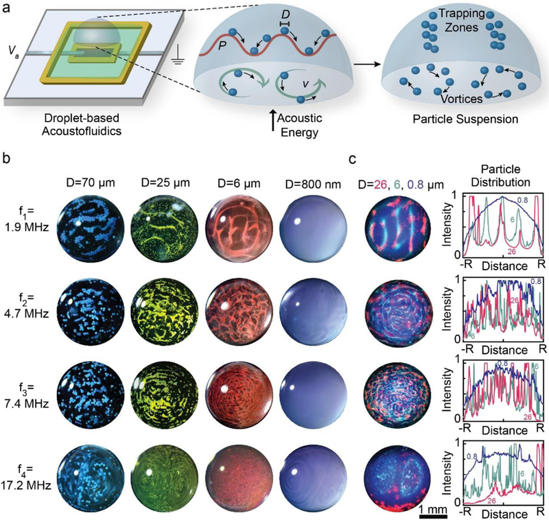
a) Schematic of droplet-based flow visualization studies using the in-plane piezoelectric transducer. Acoustic waves generated by the robotically embedded in-plane transducer propagate into the droplet producing pressure oscillations (P) and streaming flow (v) that exert forces on suspended particles (diameter = D). b) Micrographs of the suspended particle systems under excitation at each mode of the 3D printed acoustofluidic device show distinct regimes of trapping and streaming behavior for particles ranging from 0.8 – 70 μm in size. c) Fluorescence micrographs and particle distribution plots of multi-particle systems under excitation at each mode of the 3D printed acoustofluidic device show size-selective separation of particles and mode-dependent separation profiles.
3.5. Droplet-based Acoustofluidic Particle Separation Studies
The dependence of trapping patterns on particle size at a fixed frequency suggests that the in-plane transducer may provide the ability to size-selectively separate suspended particles. As shown in Figure 4c, we examined the ability to acoustically separate particles of different size using a fluorescent particle system that contained a mixture of 26, 6, and 0.8 μm particles. As shown by the fluorescence micrographs and radial intensity profiles in Figure 4c, all modes provided size-selective particle separation, yet exhibited different final configurations. As shown by comparison of Figures 4b and c, the trapping zone geometries observed for a single particle size (see Figure 4b) were consistent with those observed when particles of a different size were also present (see Figure 4c). For example, at 1.9 MHz, the 6 and 26 μm particles separated into distributed linear trapping zones, while the 800 nm particles remained relatively dispersed throughout the droplet. Alternatively, at 17.2 MHz the 6 μm particles formed symmetric ellipsoidal patterns, while the 26 μm particles became concentrated toward the droplet’s outer edge. However, it is important to note that separated particles at 1.9, 4.7, and 7.4 MHz were static, while those at 17.2 MHz were dynamic. We note that frequency-dependent dynamic particle separation profiles in droplets have also been observed using SAW devices at frequencies ranging from 10 to 130 MHz.38, 47
3.6. Integration of an Orthogonal Out-of-Plane Acoustic Transducer
Having demonstrated the functionality of the 3D printed in-plane transducers using droplet-based flow visualization studies, we next leveraged the 3D printing and pick-and-place process to construct 3D MEMS devices that contain additional orthogonal out-of-plane transducers, a novel configuration not found in SAW devices (see Figures 5a and b). As shown in Figures 5c-e, in contrast to the vacuum-based mechanism used in for embedding of the in-plane transducer (see Figure 5c), the out-of-plane transducer was embedded using an adhesion-based pick-and-place mechanism (see Figures 5d and e). As shown by the photographs in Figure 5f, the process resulted in an out-of-plane transducer that was displaced ~3 mm from the in-plane transducer. It is noteworthy that similar to a previous report using BAW transducers,52 the normal vectors of the embedded piezoelectric chip faces are orthogonal, as such configurations are difficult to achieve using SAW devices. SAW devices with multiple interdigitated electrodes that establish orthogonal pressure waves have been reported,32, 53 however, the multiple systems for actuators are typically in-plane (i.e., the normal vectors are parallel and not orthogonal) as the planar electrodes are deposited via conventional microfabrication approaches and not 3D printing as done here. We note that in addition to controlling the orientation of the integrated piezoelectric materials (e.g., in-plane vs. out-of-plane with respect to the substrate), the use of additive manufacturing offers a greater accuracy and precision with respect to integration of piezoelectric components relative to hand positioning approaches, specifically 5.7 ± 2.5 vs. 15.2 ± 3.9 % error with respect to a target position, respectively (see Figure S4 of Supporting Information). The bonding and anchoring of the piezoelectric chips to the substrate via 3D printing also improves the accuracy and precision of the fabrication process given the established control and resolution of direct-write 3D printing processes relative to manual material deposition approaches.54 Figure 5g shows the electrical impedance response of both the out-of-plane and in-plane transducers over the 0 – 20 MHz range. The orthogonal out-of-plane transducer exhibited resonant modes at 1.8 ± 0.1, 4.6 ± 0.3, 7.3 ± 0.1, and 17.2 ± 0.7 MHz (n = 5 devices), which were similar to locations of the in-plane transducer modes (see Figures 2 and 5g), suggesting that fluidic systems, such as droplets or continuously flowing liquid, could be simultaneously actuated via orthogonal in-plane and out-of-plane transducers. A detailed discussion of the origins of impedance-coupled resonant modes in anchored piezoelectric-excited millimetre-sized transducers has been reported elsewhere.43
Fig. 5.
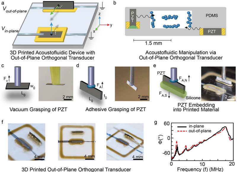
a) Schematic of a 3D microfluidic MEMS device containing two orthogonal piezoelectric chips (one in-plane and one out-of-plane). b) Concept of orienting piezoelectric transducers with both the in-plane and out-of-plane components of a microchannel using additive manufacturing to facilitate manipulation of continuously flowing particles (e.g., whole cells). c) Vacuum-based robotic embedding principle associated with integration of the in-plane piezoelectric transducer. d–e) Adhesion-based robotic embedding principle associated with integration of the out-of-plane piezoelectric transducer. f) Photographs of the device before and after printing of Ag interconnects to the out-of-plane piezoelectric transducer. g) Electrical impedance spectra of the in-plane and out-of-plane piezoelectric transducers over the 0 – 20 MHz frequency range.
3.7. Continuous Flow-based Acoustofluidic Particle Separation Studies
The data in Figure 5 suggest that 3D printing offers the ability to create 3D MEMS devices that contain multiple embedded BAW transducers with orthogonal out-of-plane configurations. Given the advantages of microfluidics regarding increased throughput and biosensing applications, we next examined the acoustofluidic effects of the 3D orthogonal transducer configuration on suspended particles in a continuous flow format. As shown in Figure 6a, a microfluidic channel printing approach based on EGaIn41 was used to construct a Y-shaped microchannel on the device in between the in-plane and out-of-plane transducer. Figure 6b shows the process resulted in a PDMS encapsulated 281 ± 11 μm wide and 197 ± 9 μm high microfluidic channel (n = 3 devices). Although the microchannel dimensions used here demonstrate the ability to interweave microfluidics within 3D MEMS via 3D printing, selection of different nozzle diameters for EGaIn printing can potentially enable matching between the transducer and the channel half-wavelength mode resonant frequencies.55 As shown schematically in Figure 6c, the fluid and suspended particles within the microchannel could be subjected to acoustic stimulation through both the in-plane and out-of-plane transducer either individually or simultaneously. Thus, we next examined the effect of these stimulation conditions on a continuously flowing suspension of 6 μm particles. Figures 6d–g show the flow profile for the following four stimulation conditions: only the in-plane transducer on at 1.9 MHz (Figure 6d), only the out-of-plane transducer on at 1.8 MHz (Figure 6e), both transducers on (Figure 6f), and both transducers off (Figure 6g), which served as the negative control. As shown in Figure 6d, stimulation using only the in-plane transducer resulted in particle concentration near the walls of the microfluidic channel. The suspended particles also exhibited a longitudinal trapping characteristic characterized by ‘strings’ of trapped particles one particle wide that extended across the width of the microchannel. In contrast as shown in Figure 6e, stimulation using only the out-of-plane transducer resulted in transverse concentration of the flowing particles toward the top of the channel causing them to leave the focal plane of the microscope. The micrograph also shows concentration of particles toward the center of the microchannel, although many of the particles remained relatively well dispersed across the microchannel width. As shown in Figure 6f, stimulation using both the in-plane and out-of-plane transducer resulted in significant particle trapping in the center of the microchannel resulting in a ~100 μm wide concentrated particle stream and surrounding disperse zone that extended ~90 μm from the wall. We note that the following observations of particle motion in the presence of acoustic stimulation differ from that observed in the absence of acoustic stimulation, which resulted in a uniformly dispersed continuously flowing suspension (see Figure 6g). Thus, the data in Figure 6d-g suggest that it is possible to move particles comparable to the size of suspended animal cells in a continuously flowing suspension in both the lateral (in-plane) and transverse (out-of-plane) direction as well as toward and away from the walls of a microfluidic channel by selective stimulation using in-plane and out-of-plane transducers, respectively. The data also show that although the PDMS-water acoustic impedance mismatch (Za,PDMS = 1.0 MRayl vs. Za,water = 1.5 MRayl) is less than silicon-water systems (Za,Si = 21.3 MRayl vs. Za,water = 1.5 MRayl),56, 57 particle trapping was still observed. The development of transparent printable materials with high acoustic impedance or PDMS-based impedance matching techniques56 could potentially improve the trapping effects. The ability to move continuously flowing suspended particles toward and away from the microchannel walls could potentially enable next-generation continuous flow-based whole cell biosensing platforms considering the walls of the microfluidic channels are often the locations of sensors. Furthermore, the ability to control the 3D orientation of acoustic transducers offers potentially novel opportunities in acoustic-based material design.58, 59
Fig. 6.
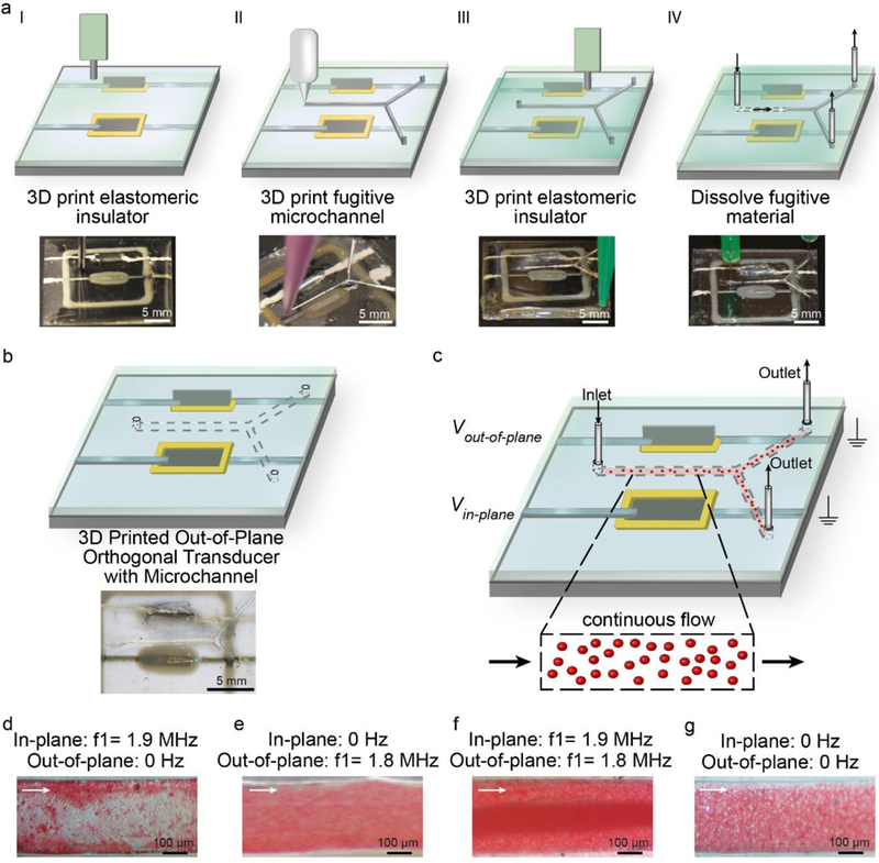
a) Schematic of the fabrication steps associated with integration of a 3D printed microchannel in between the in-plane and out-of-plane piezoelectric transducers with corresponding photographs. b) Schematic showing the microchannel orientation with respect to the integrated piezoelectric transducers and corresponding photograph after dissolution and washout of the printed eutectic Gallium-Indium. c) Schematic showing the principle of exciting both the in-plane and out-of-plane transducer during continuous flow of suspended particles through the microchannel. Flow visualization studies showing continuously flowing 6 μm particles in the presence of stimulation from the in-plane transducer (d), presence of stimulation from the out-of-plane transducer (e), presence of simultaneous stimulation from both transducers (f), and absence of acoustic stimulation (g) (white arrow indicates the direction of flow).
4. Conclusions
Here, we showed additive manufacturing processes composed of robotic pick-and-place functionality with multi-material 3D printing enable the fabrication of microfluidic-based 3D MEMS devices. We demonstrate that piezoelectric transducers could be embedded with 3D configurations consisting of orthogonal in-plane and out-of-plane configurations using a combination of vacuum- and adhesion-based embedding techniques, and showed that these transducers exhibit multiple resonant modes over the 0 – 20 MHz frequency range using electrical impedance spectroscopy. Additive manufacturing was also used to interweave microchannels between the 3D transducer configurations. We found suspended particles could be selectively concentrated in both the transverse (out-of-plane) and lateral (in-plane) directions as well as toward the walls or center of the microchannel depending on the transducer and transducer combination used for stimulation. Overall, this work suggests that additive manufacturing offers unique opportunities for the fabrication of 3D MEMS devices with 3D configurations of embedded piezoelectric components, interconnects, and microfluidic channels.
Supplementary Material
Acknowledgements
The authors are grateful for discussions and technical support from Joseph E. Dove and Carolina Tallon. BNJ is grateful for the generous support of the National Science Foundation (CBET-1650601) and the Virginia Tech Institute for Critical Technology and Applied Science (Junior Faculty Award).
Footnotes
Conflicts of interest
There are no conflicts to declare.
Electronic Supplementary Information (ESI) available. See DOI: 10.1039/x0xx00000x
References
- 1.Johnson BN, Lancaster KZ, Hogue IB, Meng F, Kong YL, Enquist LW and McAlpine MC, Lab Chip, 2016, 16, 1393–1400. [DOI] [PMC free article] [PubMed] [Google Scholar]
- 2.Kong YL, Gupta MK, Johnson BN and McAlpine MC, Nano Today, 2016, 11, 330–350. [DOI] [PMC free article] [PubMed] [Google Scholar]
- 3.Johnson BN, Lancaster KZ, Zhen G, He J, Gupta MK, Kong YL, Engel EA, Krick KD, Ju A, Meng F, Enquist LW, Jia X and McAlpine MC, Adv. Funct. Mater, 2015, 25, 6205–6217. [DOI] [PMC free article] [PubMed] [Google Scholar]
- 4.Kong YL, Tamargo IA, Kim H, Johnson BN, Gupta MK, Koh TW, Chin HA, Steingart DA, Rand BP and McAlpine MC, Nano Lett, 2014, 14, 7017–7023. [DOI] [PubMed] [Google Scholar]
- 5.Singh M, Tong Y, Webster K, Cesewski E, Haring AP, Laheri S, Carswell B, O’Brien TJ, Aardema CH, Senger RS, Robertson JL and Johnson BN, Lab Chip, 2017, 17, 2561–2571. [DOI] [PubMed] [Google Scholar]
- 6.Haring AP, Khan AU, Liu GL and Johnson BN, Adv. Opt. Mater, 2017, 5. [Google Scholar]
- 7.Macdonald E, Salas R, Espalin D, Perez M, Aguilera E, Muse D and Wicker RB, IEEE Access, 2014, 2, 234–242. [Google Scholar]
- 8.Lind JU, Busbee TA, Valentine AD, Pasqualini FS, Yuan H, Yadid M, Park SJ, Kotikian A, Nesmith AP, Campbell PH, Vlassak JJ, Lewis JA and Parker KK, Nat. Mater, 2017, 16, 303–308. [DOI] [PMC free article] [PubMed] [Google Scholar]
- 9.Gupta MK, Meng F, Johnson BN, Kong YL, Tian L, Yeh YW, Masters N, Singamaneni S and McAlpine MC, Nano Lett, 2015, 15, 5321–5329. [DOI] [PMC free article] [PubMed] [Google Scholar]
- 10.Au AK, Lee W and Folch A, Lab Chip, 2014, 14, 1294–1301. [DOI] [PMC free article] [PubMed] [Google Scholar]
- 11.Gross BC, Erkal JL, Lockwood SY, Chen C and Spence DM, Anal. Chem, 2014, 86, 3240–3253. [DOI] [PubMed] [Google Scholar]
- 12.Vaezi M, Seitz H and Yang SF, Int. J. Adv. Manuf. Technol, 2013, 67, 1721–1754. [Google Scholar]
- 13.Sreetharan PS, Whitney JP, Strauss MD and Wood RJ, J. Micromech. Microeng, 2012, 22, 055027. [Google Scholar]
- 14.Anderson KB, Lockwood SY, Martin RS and Spence DM, Anal. Chem, 2013, 85, 5622–5626. [DOI] [PubMed] [Google Scholar]
- 15.Espalin D, Muse DW, MacDonald E and Wicker RB, Int. J. Adv. Manuf. Technol, 2014, 72, 963–978. [Google Scholar]
- 16.Lopes AJ, MacDonald E and Wicker RB, Rapid Prototyping J, 2012, 18, 129–143. [Google Scholar]
- 17.Erkal JL, Selimovic A, Gross BC, Lockwood SY, Walton EL, McNamara S, Martin RS and Spence DM, Lab Chip, 2014, 14, 2023–2032. [DOI] [PMC free article] [PubMed] [Google Scholar]
- 18.Nikolaou P, Coffey AM, Walkup LL, Gust BM, LaPierre CD, Koehnemann E, Barlow MJ, Rosen MS, Goodson BM and Chekmenev EY, J. Am. Chem. Soc, 2014, 136, 1636–1642. [DOI] [PMC free article] [PubMed] [Google Scholar]
- 19.Tichem M, Lang D and Karpuschewski B, Assembly Autom, 2004, 24, 88–93. [Google Scholar]
- 20.Xie H and Regnier S, IEEE-ASME Transactions on Mechatronics, 2011, 16, 266–276. [Google Scholar]
- 21.Cedrone NJ, United States of America Pat, US4801234 A, 1989. [Google Scholar]
- 22.Zesch W, Brunner M and Weber A, Proceedings of International Conference on Robotics and Automation, Albuquerque, New Mexico: 1997. [Google Scholar]
- 23.Carlson MB, Yau KK, Simpson RE and Short MP, 3D Print. Addit. Manuf, 2015, 2, 123–130. [Google Scholar]
- 24.Henneken V, Tichem M and Karpuschewski B, Assembly Autom, 2004, 24, 416–421. [Google Scholar]
- 25.Rim YS, Bae SH, Chen H, De Marco N and Yang Y, Adv. Mater, 2016, 28, 4415–4440. [DOI] [PubMed] [Google Scholar]
- 26.Gowers SA, Curto VF, Seneci CA, Wang C, Anastasova S, Vadgama P, Yang GZ and Boutelle MG, Anal. Chem, 2015, 87, 7763–7770. [DOI] [PMC free article] [PubMed] [Google Scholar]
- 27.Ota H, Emaminejad S, Gao YJ, Zhao A, Wu E, Challa S, Chen K, Fahad HM, Jha AK, Kiriya D, Gao W, Shiraki H, Morioka K, Ferguson AR, Healy KE, Davis RW and Javey A, Adv. Mater. Tech, 2016, 1, 1600013. [Google Scholar]
- 28.Felton S, Tolley M, Demaine E, Rus D and Wood R, Science, 2014, 345, 644–646. [DOI] [PubMed] [Google Scholar]
- 29.Travitzky N, Bonet A, Dermeik B, Fey T, Filbert-Demut I, Schlier L, Schlordt T and Greil P, Adv. Eng. Mater, 2014, 16, 729–754. [Google Scholar]
- 30.Wang TM and Derby B, J. Am. Ceram. Soc, 2005, 88, 2053–2058. [Google Scholar]
- 31.Minas C, Carnelli D, Tervoort E and Studart AR, Adv. Mater, 2016, 28, 9993–9999. [DOI] [PubMed] [Google Scholar]
- 32.Ding X, Lin SC, Kiraly B, Yue H, Li S, Chiang IK, Shi J, Benkovic SJ and Huang TJ, PNAS, 2012, 109, 11105–11109. [DOI] [PMC free article] [PubMed] [Google Scholar]
- 33.Schmid L, Weitz DA and Franke T, Lab Chip, 2014, 14, 3710–3718. [DOI] [PubMed] [Google Scholar]
- 34.Voiculescu I and Nordin AN, Biosens. Bioelectron, 2012, 33, 1–9. [DOI] [PubMed] [Google Scholar]
- 35.Shilton R, Tan MK, Yeo LY and Friend JR, J. Appl. Phys, 2008, 104, 014910. [Google Scholar]
- 36.Whitehill J, Neild A, Ng TW and Stokes M, Appl. Phys. Lett, 2010, 96, 053501. [Google Scholar]
- 37.Oberti S, Neild A, Quach R and Dual J, Ultrasonics, 2009, 49, 47–52. [DOI] [PubMed] [Google Scholar]
- 38.Destgeer G, Cho H, Ha BH, Jung JH, Park J and Sung HJ, Lab Chip, 2016, 16, 660–667. [DOI] [PubMed] [Google Scholar]
- 39.Ma Z, Collins DJ and Ai Y, Anal. Chem, 2016, 88, 5316–5323. [DOI] [PubMed] [Google Scholar]
- 40.Ahn BY, Duoss EB, Motala MJ, Guo X, Park S-I, Xiong Y, Yoon J, Nuzzo RG, Rogers JA and Lewis JA, Science, 2009, 323, 1590. [DOI] [PubMed] [Google Scholar]
- 41.Parekh DP, Ladd C, Panich L, Moussa K and Dickey MD, Lab Chip, 2016, 16, 1812–1820. [DOI] [PubMed] [Google Scholar]
- 42.Sharma H, Lakshmanan RS, Johnson BN and Mutharasan R, Sens. Actuators, B, 2011, 153, 64–70. [Google Scholar]
- 43.Johnson BN and Mutharasan R, Sens. Actuators, B, 2011, 155, 868–877. [Google Scholar]
- 44.Johnson BN, Sharma H and Mutharasan R, Anal. Chem, 2013, 85, 1760–1766. [DOI] [PubMed] [Google Scholar]
- 45.Johnson BN and Mutharasan R, J. Micromech. Microeng, 2011, 21, 065027. [Google Scholar]
- 46.Johnson BN and Mutharasan R, Analyst, 2016, 142, 123–131. [DOI] [PubMed] [Google Scholar]
- 47.Destgeer G, Jung JH, Park J, Ahmed H and Sung HJ, Anal. Chem, 2017, 89, 736–744. [DOI] [PubMed] [Google Scholar]
- 48.Shilton RJ, Travagliati M, Beltram F and Cecchini M, Adv. Mater, 2014, 26, 4941–4946. [DOI] [PMC free article] [PubMed] [Google Scholar]
- 49.Destgeer G and Sung HJ, Lab Chip, 2015, 15, 2722–2738. [DOI] [PubMed] [Google Scholar]
- 50.Destgeer G, Ha B, Park J and Sung HJ, Anal. Chem, 2016, 88, 3976–3981. [DOI] [PubMed] [Google Scholar]
- 51.Friend J and Yeo LY, Rev. Mod. Phys, 2011, 83, 647–704. [Google Scholar]
- 52.Gesellchen F, Bernassau AL, Dejardin T, Cumming DRS and Riehle MO, Lab Chip, 2014, 14, 2266–2275. [DOI] [PubMed] [Google Scholar]
- 53.Yunus DE, Sohrabi S, He R, Shi WT and Liu YL, J. Micromech. Microeng, 2017, 27, 045016. [PMC free article] [PubMed] [Google Scholar]
- 54.Lewis JA and Gratson GM, Materials Today, 2004, 7, 32–39. [Google Scholar]
- 55.Lenshof A, Magnusson C and Laurell T, Lab Chip, 2012, 12, 1210–1223. [DOI] [PubMed] [Google Scholar]
- 56.Leibacher I, Schatzer S and Dual J, Lab Chip, 2014, 14, 463–470. [DOI] [PubMed] [Google Scholar]
- 57.Leibacher I, Reichert P and Dual J, Lab Chip, 2015, 15, 2896–2905. [DOI] [PubMed] [Google Scholar]
- 58.Memoli G, Caleap M, Asakawa M, Sahoo DR, Drinkwater BW and Subramanian S, Nat. Commun, 2017, 8, 14608. [DOI] [PMC free article] [PubMed] [Google Scholar]
- 59.Melde K, Mark AG, Qiu T and Fischer P, Nature, 2016, 537, 518. [DOI] [PubMed] [Google Scholar]
Associated Data
This section collects any data citations, data availability statements, or supplementary materials included in this article.