Abstract
The structural, electronic, and optical properties of heterostructures formed by transition metal dichalcogenides MX2 (M = Mo, W; X = S, Se) and graphene-like zinc oxide (ZnO) were investigated using first-principles calculations. The interlayer interaction in all heterostructures was characterized by van der Waals forces. Type-II band alignment occurs at the MoS2/ZnO and WS2/ZnO interfaces, together with the large built-in electric field across the interface, suggesting effective photogenerated-charge separation. Meanwhile, type-I band alignment occurs at the MoSe2/ZnO and WSe2/ZnO interfaces. Moreover, all heterostructures exhibit excellent optical absorption in the visible and infrared regions, which is vital for optical applications.
Introduction
Recently, transition-metal dichalcogenides (TMDs) have attracted much attention because of their interesting electronic1,2, mechanical3, thermal4,5, and optical6 properties. Their monolayers can be prepared by either mechanical exfoliation or chemical growth7. Investigations on the application of TMDs in nanoelectronics8,9, catalysis10,11, spintronics12,13, and valleytronics14,15 indicate that TMDs are a category of very promising two-dimensional (2D) materials.
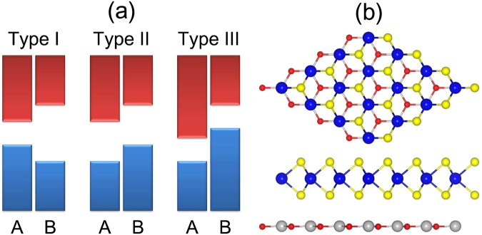
At the same time, the formation of 2D van der Waals (vdW) heterostructures has been widely adopted to tune the properties of 2D materials. The vdW heterostructure has been extensively investigated in theoretical and experimental studies16–28, and the band alignments at the interface of a semiconducting vdW heterostructure are found to be vital for its applications. Heterostructures can be divided into three types according to the band alignment: type I (symmetric), type II (staggered), or type III (broken)29, as shown in Fig. 1(a). In a type-I heterostructure, the conduction band minimum (CBM) and the valence band maximum (VBM) of two composite layers (A and B) obey the following rule: VBMB < VBMA < CBMA < CBMB. Since the VBM and CBM of a type-I heterostructure are located in one layer, efficient recombination of the photogenerated electrons and holes can occur when it is irradiated by light. Therefore, type-I heterostructures have been widely used in optical devices such as light-emitting diodes (LEDs)30. In contrast, in a type-II heterostructure, the CBM and the VBM of two composite layers (A and B) obey the following rule: VBMA < VBMB < CBMA < CBMB. Therefore, the VBM and CBM of a type-II heterostructure exist in different layers. Since the photogenerated electron–hole pairs can be split at the interface, with electrons transferred to one layer and the holes to the other, this heterostructure has been demonstrated to be a fundamental component of photovoltaic devices. For example, Bernardi et al.31 investigated the photovoltaic devices based on a MoS2/WS2 bilayer, they revealed that the MoS2 and WS2 monolayers form a type-II heterostructure, which can yield a power-conversion efficiency of up to ∼1% and much higher power densities than existing ultrathin solar cells. On the other hand, in a type-III heterostructure, the CBM and the VBM of two composite layers (A and B) obey the following rule: VBMA < CBMA < VBMB < CBMB. Type-III heterostructures have been successfully applied in tunnelling field-effect transistors32. As described earlier, in addition to being an interesting research topic, the formation of vdW heterostructures by TMDs and other materials can widen the application of TMDs.
Figure 1.
(a) Schematic presentation of type-I, type-II, and type-III heterostructures; the conduction bands are shown in red, and the valence bands are shown in blue. (b) Schematic illustration of crystal structures of the MX2/ZnO heterostructure; the red, yellow, grey, and blue spheres represent M, X, Zn, and O atoms, respectively.
Graphene-like ZnO (ZnO) is also a widely investigated 2D semiconducting material33–36. Moreover, ZnO layers have been experimentally synthesized37–39. In the study reported here, we designed four different MX2/ZnO heterostructures: MoS2/ZnO, WS2/ZnO, MoSe2/ZnO, and WSe2/ZnO. The structural, electronic, and optical properties of these heterostructures were investigated.
The lattice parameters of MoS2, WS2, MoSe2, WSe2, and ZnO are 3.16, 3.17, 3.29, 3.29, and 3.29 Å, respectively. The bandgaps of MoS2, MoSe2, WS2, WSe2 and ZnO are 2.24, 2.37, 1.99, 2.12 and 3.29 eV respectively, and they are all direct-bandgap semiconductors. In an earlier study, Defo et al.40 demonstrated that the electronic properties of MX2 are rather sensitive to strain. Therefore, we chose to vary the lattice constant of ZnO and fix the lattice constants of MX2 for constructing the heterostructures. The interlayer lattice mismatches in the MoS2/ZnO and WS2/ZnO heterostructures are 4.11% and 3.79% respectively, which are quite small. For each MX2/ZnO heterostructure, several possible stacking patterns were examined (Fig. S1 in Supporting Information). Interestingly, all of the heterostructures favour the same stacking pattern, as shown in Fig. 1(b). The binding energy is defined as , where , EZnO, and are the total energy of MX2, ZnO, and the MX2/ZnO heterostructure, respectively. The binding energy of the MoS2/ZnO, WS2/ZnO, MoSe2/ZnO and WSe2/ZnO heterostructures are 269, 264, 285 and 282 meV respectively, while the corresponding interlayer distances are 2.91, 2.98, 2.89 and 2.89 Å respectively, indicating the typical vdW nature of the interaction between the two layers.
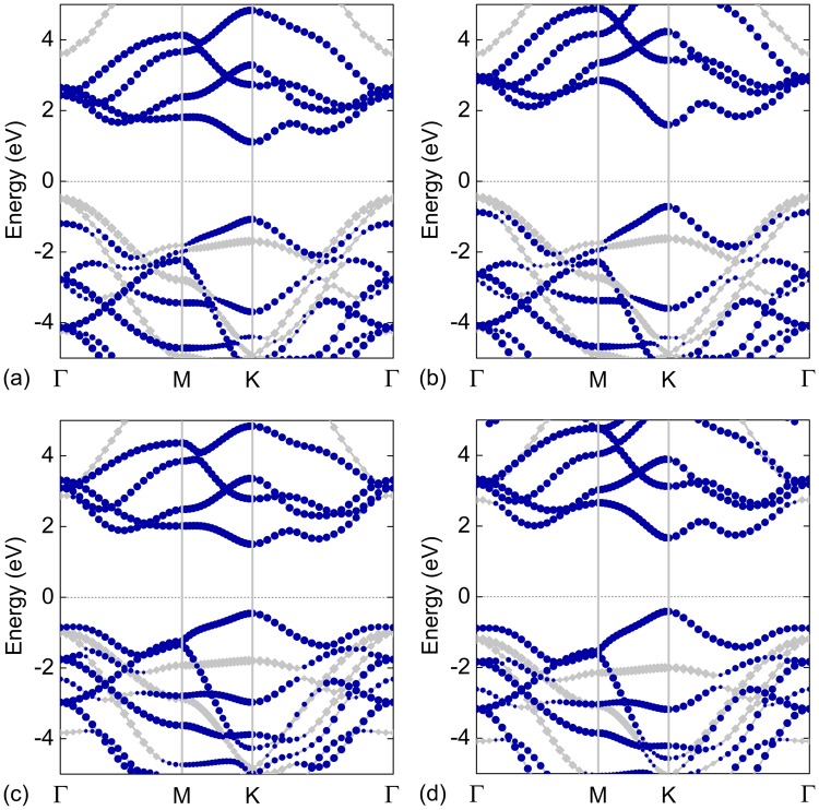
The projected band structures of the MoS2/ZnO, WS2/ZnO, MoSe2/ZnO, and WSe2/ZnO vdW heterostructures are shown in Fig. 2. These heterostructures can be divided into two categories. The first category includes the MoS2/ZnO and WS2/ZnO heterostructures, both of which have a type-II band alignment. They are semiconductors with indirect bandgaps of 1.60 and 2.05 eV, respectively. The CBM and VBM of the MoS2/ZnO (or WS2/ZnO) heterostructure are predominately contributed by the MoS2 (or WS2) and ZnO layers respectively. The second category includes the MoSe2/ZnO and WSe2/ZnO heterostructures, both of which have a type-I band alignment. Both the CBM and VBM of MoSe2/ZnO and WSe2/ZnO heterostructures are located at the K point in BZ, which suggest that they are direct-bandgap semiconductors. The bandgaps of MoSe2/ZnO and WSe2/ZnO heterostructures are 1.96 and 2.08 eV, respectively. Moreover, both the CBM and VBM of these two heterostructures originate from the TMD layer.
Figure 2.
Projected band structures of the MoS2/ZnO, WS2/ZnO, MoSe2/ZnO, and WSe2/ZnO vdW heterostructures; the royal and grey symbols represent the contribution of MX2 and ZnO, respectively; the Fermi level is set to zero, and it is indicated by the black dashed line.
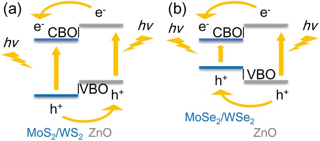
Previously, many reports41–43 suggested that MoS2 and WS2 have the potential for application in photocatalysts for water splitting. The main obstacle to obtain a high-efficiency photocatalyst is the problem of electron–hole recombination. In the MoS2/ZnO and WS2/ZnO heterostructures, the conduction-band offset (CBO) and valence-band offset (VBO) between the MoS2 (or WS2) and ZnO layers are approximately 2.49 (or 2.00) and 0.58 (or 0.26) eV respectively, as shown in Fig. 3(a). Driven by the CBO, the photogenerated electrons in ZnO tend to move to the CB of the MoS2 (or WS2) layer, while the photogenerated holes in the MoS2 (or WS2) layer are readily migrate to the VB of the ZnO layer with the assistance of the VBO. Therefore, the problem of electron–hole recombination can be overcome with these band offsets.
Figure 3.
Schematic illustration of the migration of photogenerated electrons and holes at the (a) MoS2/ZnO and WS2/ZnO interfaces; and the (b) MoSe2/ZnO and WSe2/ZnO interfaces.
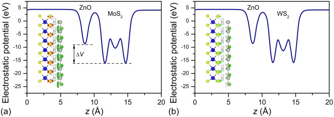
The built-in electric field plays an important role in determining the catalytic activity of a photocatalyst because a large built-in electric field can further boost the migration of photogenerated charges. The insets in Fig. 4 present the isosurfaces of charge difference of the MoS2/ZnO and WS2/ZnO vdW heterostructures. The ZnO layer always acts as a donor. The transferred charge is 0.016 (or 0.012) |e| for the MoS2/ZnO (or WS2/ZnO) vdW heterostructure according to the Bader charge-population analysis44–46, which can induce a large potential drop across the interface of the heterostructure, as shown in Fig. 4. The potential drop across the MoS2/ZnO (or WS2/ZnO interface) is 7.38 (or 7.33) eV, which can induce a large built-in electric field from the MoS2 (or WS2) layer to the ZnO layer, and this field should exert some effect on the photogenerated electron–hole recombination in the MoS2/ZnO (or WS2/ZnO) vdW heterostructure.
Figure 4.
Potential drop across the interface of the (a) MoS2/ZnO and (b) WS2/ZnO vdW heterostructure. The isosurface of charge difference (set to 0.003 e/Å3) is also shown in the corresponding figure; the yellow and cyan regions denote the gain and loss of electrons, respectively.
The CBO and VBO in the MoSe2/ZnO and WSe2/ZnO heterostructures also play an important role. As shown in Fig. 3(b), the CBO and VBO in the MoSe2/ZnO (or WSe2/ZnO) heterostructure are 1.37 (or 1.07) and 0.53 (or 0.78) eV, respectively. With these band offsets, both the photogenerated electrons and holes tend to move from the ZnO to the TMD layer, while the photogenerated electrons and holes in the TMD layer are prohibited from escaping. Thus, the photogenerated electrons and holes tend to recombine again, which would be a useful feature for optical devices such as LEDs30.
The imaginary parts of the dielectric functions of the MoS2/ZnO, WS2/ZnO, MoSe2/ZnO, and WSe2/ZnO vdW heterostructures are shown in Fig. 5. All the heterostructures show good ability to absorb light in the visible and near-infrared (NIR) regions, which is evident from the high absorption peaks at approximately 488, 555, 441, and 498 nm in the visible region of their respective spectra. Since the wavelengths of light arriving at the earth are mainly in the visible and NIRregions47, these heterostructures are promising components for various optical, photovoltaic and photocatalytic applications.
Figure 5.
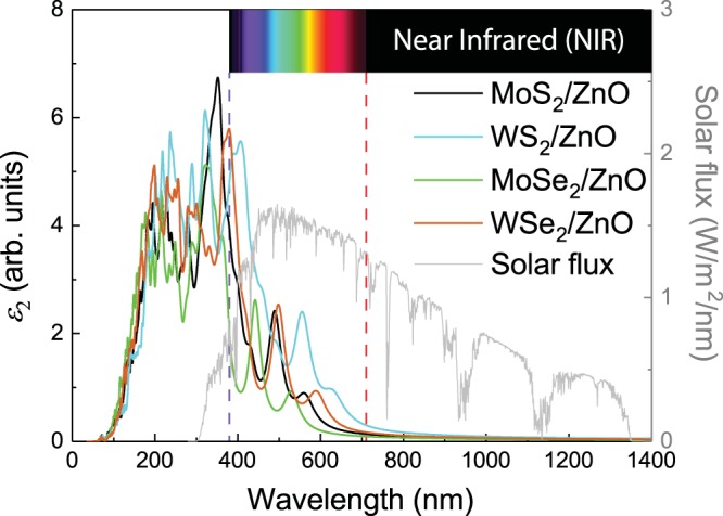
Imaginary parts of dielectric constants of the MoS2/ZnO, WS2/ZnO, MoSe2/ZnO, and WSe2/ZnO vdW heterostructures; the range of light absorption by each heterostructure overlaps the wavelength range of the incident AM1.5 G solar flux.
In summary, the structural, electronic, and optical properties of the MoS2/ZnO, WS2/ZnO, MoSe2/ZnO, and WSe2/ZnO vdW heterostructures were systematically investigated using first-principles calculations. The interactions at all the TMD/ZnO interfaces are dominated by vdW forces. The MoS2/ZnO and WS2/ZnO vdW heterostructures are indirect-bandgap semiconductors with bandgaps of 1.60 and 2.05 eV, respectively. The CBM is contributed by the TMD layer, while the VBM is contributed by the ZnO layer, indicating the formation of a type-II heterostructure, which can promote the separation of photogenerated electron–hole pairs. Moreover, large built-in electric fields are stabilized at both the MoS2/ZnO and WS2/ZnO interfaces, which will further separate the photogenerated charges. On the other hand, the MoSe2/ZnO and WSe2/ZnO vdW heterostructures are direct-bandgap semiconductors with bandgaps of 1.96 and 2.08 eV respectively. Both the CBM and VBM originate from the TMD layer, thus a type-I heterostructure is formed. In addition, the MoS2/ZnO, WS2/ZnO, MoSe2/ZnO, and WSe2/ZnO vdW heterostructures are all high solar-flux collectors. Therefore, these hetersotructures have great potential for application in optical, photovoltaic, and photocatalytic devices.
Methods
First-principles calculations were carried out by using the Vienna Ab Initio Simulation Package48, which is based on the density functional theory (DFT) in a plane-wave basis set with the projector-augmented wave method49. For the exchange-correlation functional, the generalized gradient approximation of Perdew, Burke, and Ernzerhof 50,51 was used to obtain the geometric structures, while the Heyd–Scuseria–Ernzerhof hybrid functional52,53 was used to calculate the electronic and optical properties. The DFT-D3 method of Grimme54 was used to account for the dispersion forces. The energy cutoff for plane-wave expansion was set to 550 eV, and the first Brillouin zone was sampled by a 21 × 21 × 1 Monkhorst–Pack55 k-point grid. The thickness of the vacuum region was set to 20 Å to avoid interference between the periodic images. All the structures were fully relaxed until the Hellmann–Feynman force on each atom was <0.01 eV/Å.
Electronic supplementary material
Acknowledgements
This study was funded by the National Science Foundation for Young Scientists of China (grant number 11704165), the Science Foundation of Guizhou Science and Technology Department (grant number QKHJZ[2015]2150), the Science Foundation of Guizhou Provincial Education Department (grant number QJHKYZ[2016]092), as well as the Science Foundation of Jinling Institute of Technology (grant number 40620064). Minglei Sun hopes to express his gratitude to the support of Miss Yujing Xu over years, and the encouragement of Miss Dulko and Miss Tolmach in Singapore.
Author Contributions
M.S. designed the project. S.W. and M.S. wrote the main manuscript text and prepared all figures. H.T., C.R., and J.Y. contributed detailed discussions. All authors reviewed the manuscript.
The authors declare no competing interests.
Footnotes
Publisher's note: Springer Nature remains neutral with regard to jurisdictional claims in published maps and institutional affiliations.
Contributor Information
Sake Wang, Email: IsaacWang@jit.edu.cn.
Minglei Sun, Email: mingleisun@outlook.com.
Electronic supplementary material
Supplementary information accompanies this paper at 10.1038/s41598-018-30614-3.
References
- 1.Wickramaratne D, Zahid F, Lake RK. Electronic and thermoelectric properties of few-layer transition metal dichalcogenides. J. Chem. Phys. 2014;140:124710. doi: 10.1063/1.4869142. [DOI] [PubMed] [Google Scholar]
- 2.Cai Y, Zhang G, Zhang Y-W. Polarity-reversed robust carrier mobility in monolayer MoS2 nanoribbons. J. Am. Chem. Soc. 2014;136:6269–6275. doi: 10.1021/ja4109787. [DOI] [PubMed] [Google Scholar]
- 3.Li J, Medhekar NV, Shenoy VB. Bonding charge density and ultimate strength of monolayer transition metal dichalcogenides. J. Phys. Chem. C. 2013;117:15842–15848. doi: 10.1021/jp403986v. [DOI] [Google Scholar]
- 4.Cai Y, Lan J, Zhang G, Zhang Y-W. Lattice vibrational modes and phonon thermal conductivity of monolayer MoS2. Phys. Rev. B. 2014;89:035438. doi: 10.1103/PhysRevB.89.035438. [DOI] [Google Scholar]
- 5.Zhang G, Zhang Y-W. Thermoelectric properties of two-dimensional transition metal dichalcogenides. J. Mater. Chem. C. 2017;5:7684–7698. doi: 10.1039/C7TC01088E. [DOI] [Google Scholar]
- 6.Shi H, Pan H, Zhang Y-W, Yakobson BI. Quasiparticle band structures and optical properties of strained monolayer MoS2 and WS2. Phys. Rev. B. 2013;87:155304. doi: 10.1103/PhysRevB.87.155304. [DOI] [Google Scholar]
- 7.Huang X, Zeng Z, Zhang H. Metal dichalcogenide nanosheets: preparation, properties and applications. Chem. Soc. Rev. 2013;42:1934–1946. doi: 10.1039/c2cs35387c. [DOI] [PubMed] [Google Scholar]
- 8.Radisavljevic B, Radenovic A, Brivio J, Giacometti V, Kis A. Single-layer MoS2 transistors. Nat. Nano. 2011;6:147. doi: 10.1038/nnano.2010.279. [DOI] [PubMed] [Google Scholar]
- 9.Cui Y, et al. High‐performance monolayer Ws2 field-effect transistors on high-κ dielectrics. Adv. Mater. 2015;27:5230–5234. doi: 10.1002/adma.201502222. [DOI] [PubMed] [Google Scholar]
- 10.Voiry D, et al. The role of electronic coupling between substrate and 2D MoS2 nanosheets in electrocatalytic production of hydrogen. Nat. Mater. 2016;15:1003 EP. doi: 10.1038/nmat4660. [DOI] [PubMed] [Google Scholar]
- 11.Liu Y, et al. Self-optimizing, highly surface-active layered metal dichalcogenide catalysts for hydrogen evolution. Nat. Energy. 2017;2:17127. doi: 10.1038/nenergy.2017.127. [DOI] [Google Scholar]
- 12.Cheng YC, Zhu ZY, Mi WB, Guo ZB, Schwingenschlögl U. Prediction of two-dimensional diluted magnetic semiconductors: Doped monolayer MoS2 systems. Phys. Rev. B. 2013;87:100401. doi: 10.1103/PhysRevB.87.100401. [DOI] [Google Scholar]
- 13.Feng N, et al. First principles prediction of the magnetic properties of Fe-X6 (X = S, C, N, O, F) doped monolayer MoS2. Sci. Rep. 2014;4:3987. doi: 10.1038/srep03987. [DOI] [PMC free article] [PubMed] [Google Scholar]
- 14.Jones AM, et al. Optical generation of excitonic valley coherence in monolayer WSe2. Nat. Nano. 2013;8:634. doi: 10.1038/nnano.2013.151. [DOI] [PubMed] [Google Scholar]
- 15.Peng B, et al. Valley polarization of trions and magnetoresistance in heterostructures of MoS2 and yttrium iron garnet. ACS Nano. 2017;11:12257–12265. doi: 10.1021/acsnano.7b05743. [DOI] [PubMed] [Google Scholar]
- 16.Sun M, et al. Tunable Schottky barrier in van der Waals heterostructures of graphene and g-GaN. Appl. Phys. Lett. 2017;110:173105. doi: 10.1063/1.4982690. [DOI] [Google Scholar]
- 17.Zhang C, et al. Systematic study of electronic structure and band alignment of monolayer transition metal dichalcogenides in Van der Waals heterostructures. 2D Mater. 2017;4:015026. doi: 10.1088/2053-1583/4/1/015026. [DOI] [Google Scholar]
- 18.Sun M, Chou J-P, Yu J, Tang W. Electronic properties of blue phosphorene/graphene and blue phosphorene/graphene-like gallium nitride heterostructures. Phys. Chem. Chem. Phys. 2017;19:17324–17330. doi: 10.1039/C7CP01852E. [DOI] [PubMed] [Google Scholar]
- 19.You B, Wang X, Zheng Z, Mi W. Black phosphorene/monolayer transition-metal dichalcogenides as two dimensional van der Waals heterostructures: a first-principles study. Phys. Chem. Chem. Phys. 2016;18:7381–7388. doi: 10.1039/C5CP07585H. [DOI] [PubMed] [Google Scholar]
- 20.Song Y, Li D, Mi W, Wang X, Cheng Y. Electric field effects on spin splitting of two-dimensional van der Waals arsenene/FeCl2 heterostructures. J. Phys. Chem. C. 2016;120:5613–5618. doi: 10.1021/acs.jpcc.6b01062. [DOI] [Google Scholar]
- 21.Zhang X, et al. Computational screening of 2D materials and rational design of heterojunctions for water splitting photocatalysts. Small Methods. 2018;2:1700359. doi: 10.1002/smtd.201700359. [DOI] [Google Scholar]
- 22.Sun M, Chou J-P, Yu J, Tang W. Effects of structural imperfection on the electronic properties of graphene/WSe2 heterostructures. J. Mater. Chem. C. 2017;5:10383–10390. doi: 10.1039/C7TC03131A. [DOI] [Google Scholar]
- 23.Koda DS, Bechstedt F, Marques M, Teles LK. Tuning electronic properties and band alignments of phosphorene combined with MoSe2 and WSe2. J. Phys. Chem. C. 2017;121:3862–3869. doi: 10.1021/acs.jpcc.6b10976. [DOI] [Google Scholar]
- 24.Sun M, Chou J-P, Zhao Y, Yu J, Tang W. Weak C-H…F-C hydrogen bonds make a big difference in graphane/fluorographane and fluorographene/fluorographane bilayers. Phys. Chem. Chem. Phys. 2017;19:28127–28132. doi: 10.1039/C7CP04535B. [DOI] [PubMed] [Google Scholar]
- 25.Lee C-H, et al. Atomically thin p–n junctions with van der Waals heterointerfaces. Nat. Nano. 2014;9:676. doi: 10.1038/nnano.2014.150. [DOI] [PubMed] [Google Scholar]
- 26.Gong Y, et al. Vertical and in-plane heterostructures from WS2/MoS2 monolayers. Nat. Mater. 2014;13:1135. doi: 10.1038/nmat4091. [DOI] [PubMed] [Google Scholar]
- 27.Tongay S, et al. Tuning interlayer coupling in large-area heterostructures with CVD-grown MoS2 and WS2 monolayers. Nano Lett. 2014;14:3185–3190. doi: 10.1021/nl500515q. [DOI] [PubMed] [Google Scholar]
- 28.Rivera P, et al. Observation of long-lived interlayer excitons in monolayer MoSe2–WSe2 heterostructures. Nat. Commun. 2015;6:6242. doi: 10.1038/ncomms7242. [DOI] [PubMed] [Google Scholar]
- 29.Özçelik VO, Azadani JG, Yang C, Koester SJ, Low T. Band alignment of two-dimensional semiconductors for designing heterostructures with momentum space matching. Phys. Rev. B. 2016;94:035125. doi: 10.1103/PhysRevB.94.035125. [DOI] [Google Scholar]
- 30.Nakamura S, Senoh M, Iwasa N. & Nagahama, S.-i. High-brightness InGaN blue, green and yellow light-emitting diodes with quantum well structures. Jpn. J. Appl. Phys. 1995;34:L797. doi: 10.1143/JJAP.34.L797. [DOI] [Google Scholar]
- 31.Bernardi M, Palummo M, Grossman JC. Extraordinary sunlight absorption and one nanometer thick photovoltaics using two-dimensional monolayer materials. Nano Lett. 2013;13:3664–3670. doi: 10.1021/nl401544y. [DOI] [PubMed] [Google Scholar]
- 32.Koswatta SO, Koester SJ, Haensch W. On the possibility of obtaining MOSFET-like performance and sub-60-mV/dec swing in 1-D broken-gap tunnel transistors. IEEE T. Electron Dev. 2010;57:3222–3230. doi: 10.1109/TED.2010.2079250. [DOI] [Google Scholar]
- 33.Tang Q, Li Y, Zhou Z, Chen Y, Chen Z. Tuning electronic and magnetic properties of wurtzite ZnO nanosheets by surface hydrogenation. ACS Appl. Mater. Interfaces. 2010;2:2442–2447. doi: 10.1021/am100467j. [DOI] [PubMed] [Google Scholar]
- 34.Topsakal M, Cahangirov S, Bekaroglu E, Ciraci S. First-principles study of zinc oxide honeycomb structures. Phys. Rev. B. 2009;80:235119. doi: 10.1103/PhysRevB.80.235119. [DOI] [Google Scholar]
- 35.Botello-Méndez AR, López-Urías F, Terrones M, Terrones H. Magnetic behavior in zinc oxide zigzag nanoribbons. Nano Lett. 2008;8:1562–1565. doi: 10.1021/nl072511q. [DOI] [PubMed] [Google Scholar]
- 36.Kou L, Li C, Zhang Z, Guo W. Tuning magnetism in zigzag ZnO nanoribbons by transverse electric fields. ACS Nano. 2010;4:2124–2128. doi: 10.1021/nn901552b. [DOI] [PubMed] [Google Scholar]
- 37.Tusche C, Meyerheim HL, Kirschner J. Observation of depolarized ZnO(0001) monolayers: formation of unreconstructed planar sheets. Phys. Rev. Lett. 2007;99:026102. doi: 10.1103/PhysRevLett.99.026102. [DOI] [PubMed] [Google Scholar]
- 38.Schott V, et al. Chemical activity of thin oxide layers: strong interactions with the support yield a new thin-film phase of ZnO. Angew. Chem. Int. Ed. 2013;52:11925–11929. doi: 10.1002/anie.201302315. [DOI] [PubMed] [Google Scholar]
- 39.Quang HT, et al. In Situ Observations of free-standing graphene-like mono- and bilayer ZnO membranes. ACS Nano. 2015;9:11408–11413. doi: 10.1021/acsnano.5b05481. [DOI] [PubMed] [Google Scholar]
- 40.Defo RK, et al. Strain dependence of band gaps and exciton energies in pure and mixed transition-metal dichalcogenides. Phys. Rev. B. 2016;94:155310. doi: 10.1103/PhysRevB.94.155310. [DOI] [Google Scholar]
- 41.Zhuang HL, Hennig RG. Computational search for single-layer transition-metal dichalcogenide photocatalysts. J. Phys. Chem. C. 2013;117:20440–20445. doi: 10.1021/jp405808a. [DOI] [Google Scholar]
- 42.Kang J, Tongay S, Zhou J, Li J, Wu J. Band offsets and heterostructures of two-dimensional semiconductors. Appl. Phys. Lett. 2013;102:012111. doi: 10.1063/1.4774090. [DOI] [Google Scholar]
- 43.Kumar R, Das D, Singh AK. C2N/WS2 van der Waals type-II heterostructure as a promising water splitting photocatalyst. J. Catal. 2018;359:143–150. doi: 10.1016/j.jcat.2018.01.005. [DOI] [Google Scholar]
- 44.Henkelman G, Arnaldsson A, Jónsson H. A fast and robust algorithm for Bader decomposition of charge density. Comput. Mater. Sci. 2006;36:354–360. doi: 10.1016/j.commatsci.2005.04.010. [DOI] [Google Scholar]
- 45.Sanville E, Kenny SD, Smith R, Henkelman G. Improved grid-based algorithm for Bader charge allocation. J. Comput. Chem. 2007;28:899–908. doi: 10.1002/jcc.20575. [DOI] [PubMed] [Google Scholar]
- 46.Tang W, Sanville E, Henkelman G. A grid-based Bader analysis algorithm without lattice bias. J. Phys.: Condens. Matter. 2009;21:084204. doi: 10.1088/0953-8984/21/8/084204. [DOI] [PubMed] [Google Scholar]
- 47.Reference Solar Spectral Irradiance: Air Mass 1.5. Available at http://rredc.nrel.gov/solar/spectra/am1.5.
- 48.Kresse G, Furthmüller J. Efficiency of ab-initio total energy calculations for metals and semiconductors using a plane-wave basis set. Comput. Mater. Sci. 1996;6:15–50. doi: 10.1016/0927-0256(96)00008-0. [DOI] [PubMed] [Google Scholar]
- 49.Kresse G, Joubert D. From ultrasoft pseudopotentials to the projector augmented-wave method. Phys. Rev. B. 1999;59:1758–1775. doi: 10.1103/PhysRevB.59.1758. [DOI] [Google Scholar]
- 50.Perdew JP, Burke K, Ernzerhof M. Generalized gradient approximation made simple. Phys. Rev. Lett. 1996;77:3865–3868. doi: 10.1103/PhysRevLett.77.3865. [DOI] [PubMed] [Google Scholar]
- 51.Perdew JP, Burke K, Ernzerhof M. Generalized gradient approximation made simple [Phys. Rev. Lett. 77, 3865 (1996)] Phys. Rev. Lett. 1997;78:1396. doi: 10.1103/PhysRevLett.78.1396. [DOI] [PubMed] [Google Scholar]
- 52.Heyd J, Scuseria GE, Ernzerhof M. Hybrid functionals based on a screened Coulomb potential. J. Chem. Phys. 2003;118:8207–8215. doi: 10.1063/1.1564060. [DOI] [Google Scholar]
- 53.Heyd J, Scuseria GE, Ernzerhof M. Erratum: Hybrid functionals based on a screened Coulomb potential [J. Chem. Phys. 118, 8207 (2003)] J. Chem. Phys. 2006;124:219906. doi: 10.1063/1.2204597. [DOI] [Google Scholar]
- 54.Grimme S, Antony J, Ehrlich S, Krieg H. A consistent and accurate ab initio parametrization of density functional dispersion correction (DFT-D) for the 94 elements H-Pu. J. Chem. Phys. 2010;132:154104. doi: 10.1063/1.3382344. [DOI] [PubMed] [Google Scholar]
- 55.Monkhorst HJ, Pack JD. Special points for Brillouin-zone integrations. Phys. Rev. B. 1976;13:5188–5192. doi: 10.1103/PhysRevB.13.5188. [DOI] [Google Scholar]
Associated Data
This section collects any data citations, data availability statements, or supplementary materials included in this article.


