Abstract
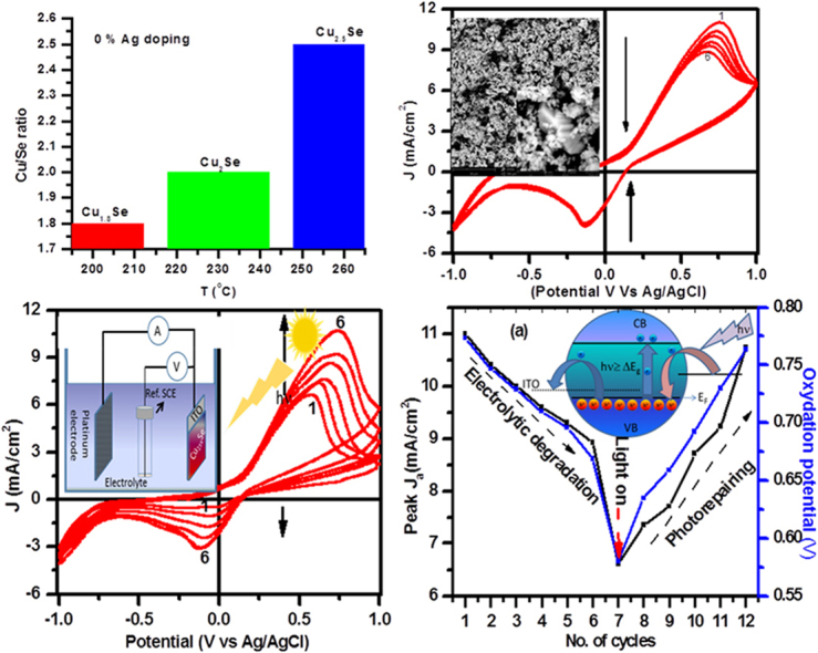
In nature, self-healing can be induced by sunlight for damage and wound repair, and this phenomenon is very important to living species for prolonging their lives. This self-repairing feature is obviously highly desirable for non-biological materials and manmade systems. In this paper, we demonstrate, for the first time, that battery electrodes can be self-repaired when exposed to sunlight. Here, we show that the optical, and photoelectrochemical (PEC) properties can be controlled by varying structural and compositional parameters of copper selenide nanocrystals (NCs). Cation to anion ratio in copper selenide (Cu2±xSe) NCs can be controlled over a wide range of 1.3–2.7 by simply changing the reaction temperature and impurity. Light-induced self-repairable behavior is demonstrated with electrochemical (EC) and PEC performances of electrodes made with stoichiometric copper selenide NCs. This nature-inspired, self-repairing behavior can be applied to batteries, supercapacitors, and photo-electrochemical fuel generators.
Keywords: Copper selenide, Self-repairable electrodes, Localized surface plasmon resonance, Compositional control, Free charge carrier density, Photo-electrochemical
Graphical abstract
Highlights
-
•
The first demonstration of light-induced self-reparability in battery electrodes.
-
•
Demonstration of a scalable method for copper selenide nanocrystals.
-
•
Temperature and impurity are keys to control structural and compositional properties.
-
•
Tunability in localized Surface Plasmon Resonance and free carrier density.
1. Introduction
Today, an average person throws away eight batteries per year thus millions of batteries are wasted imposing an immeasurable, adverse effect on our environment [1]. In nature, self-repairing is an important feature for living species, where wounds are self-healed to restore physiological functions and extend the life of an organism. Sunlight is an important self-repairing activator in plants and animals, where photons are absorbed through electronic absorption of some molecular chromophores or photoacceptors, which turns on intensified physiological activities to repair wounds [2]. Inspired by this phenomenon, it is highly desirable to incorporate self-reparability features in energy harvesting, e.g. electrochemical cells, as well as in energy storage devices, e.g. batteries and capacitors, to prolong their lifetime. Electrochemical reactions at electrode-electrolyte interfaces in batteries result in the structural and compositional changes in electrode material due to the irreversible redox reaction that causes degradation in device performance over the course of a number of cycles and ultimately resulting in its failure [3], [4]. Therefore, self-reparability features require structural and compositional control of the electrode material over many cycles to ensure its prolonged operation.
Recently, copper chalcogenides have attracted extensive research due to their fascinating physical, chemical, and semiconducting properties driven by their chemical composition and crystalline structure, which are tailorable through intelligent control of synthesis conditions [5], [6], [7], [8], [9], [10]. Copper selenide (Cu2Se) is an important chalcogenide material with a wide range of applications in thermoelectric and photovoltaic-based energy harvesting [11], [12], [13], in photocatalytic degradation of dyes for water purification, in the fabrication of electrodes for batteries [14], [15], and in photo-ablation therapy [16]. Due to their metal-like behavior, copper selenide nanocrystals (NCs) have strong localized surface plasmon resonance (LSPR) absorption tunable by their size, shape, and chemical composition [17], [18]. Strong and widely tunable LSPRs in near and mid-infrared spectral regions make copper selenide an ideal candidate for solar energy harvesting, photodetector and plasmonic sensing applications.
Elemental composition is a decisive parameter for copper selenide NCs that control their crystalline structure and electronic behavior [19] and hence self-repairable capability. For example, bulk and stoichiometric copper selenide (Cu2Se) is a zero bandgap material with metal-like behavior [20]. However, copper-deficient Cu2-xSe is an intrinsic p-type semiconductor with direct and indirect bandgap energies in the range of 2.1–2.3 eV and 1.2–1.4 eV, respectively [14], [19], [20]. Non-stoichiometry in Cu2±xSe NCs affects their electronic properties and significantly alters their crystalline structure and cation exchange properties [21], [22], [23]. Not only composition, but the arrangement of atoms in a given structural phase is also a crucial parameter to control electronic, thermal, and chemical properties of copper selenide [20], [21], [22], [23]. For example, Pb+2 ions selectively react with different planes of cubic and hexagonal stoichiometric Cu2Se NCs in cation exchange reactions [24]. Owing to these magnificent characteristics, compositional and structural control in copper selenide NCs is highly desirable for their specific scientific and technological applications, which poses a general challenge for researchers to discover new synthesis methodologies.
Typical methodology discovery is conducted with conventional solution chemistry, where either the concentration of chemical precursors is varied [25], or post-processing techniques, such as cation exchange or thermal annealing, are used to control chemical composition or crystallinity/phase of materials [24], [26], [27]. In the former case, the amount of required precursor needs to be calculated and measured precisely for a given chemical composition. However, the latter involves multiple additional time-consuming steps that increase the possibility of contamination and environmental exposure. For example, annealing of the sample at a high temperature for phase conversion might oxidize it and limit its device applications.
In this work, we report reaction temperature and impurity-induced structural and compositional control in gram scale synthesis of Cu2±xSe NCs for light-induced self-repairable electrodes for electrochemical cells. The reaction temperature is varied from 200 to 260 °C to tune the copper to selenium ratio from 1.8 to 2.5 while retaining their α-crystalline phase. Doping of silver is also used to control compositional properties as well as the crystalline structure of copper selenide NCs. At a given reaction temperature (230 °C), 1% w/w doping of Ag transfers stoichiometric (α-Cu2Se) copper selenide NCs to non-stoichiometric (α-Cu2.7Se) selenium deficient NCs of the same crystalline phase, while 2% doping of silver causes compositional and phase transformation to produce non-stoichiometric β-phase of copper selenide (β-Cu1.3Se) NCs. Stoichiometric α-Cu2Se and non-stoichiometric β-Cu1.3Se NCs are tested for EC and PEC performance. Interestingly, we observed light-induced self-repairable behavior for an electrode made with copper selenide NCs having Cu/Se ratio close to its stoichiometric value. In the dark, an electrode made from stoichiometric copper selenide NCs shows a decrease in anodic current density as well as a decrease in the value of oxidation potential with the number of cycles (degradation). However, under illumination with a solar simulator, it re-attains its initial state of current density and oxidation potential (i.e. light induced self-repairing under solar light) after the same number of cycles.
2. Experimental section
2.1. Synthesis of copper selenide nanocrystals
2.1.1. Materials
Copper oxide (CuO; 99.95%), selenium oxide (SeO2; 99.97%), silver oxide (AgO;99.97%), sodium hydroxide (NaOH; 99.97%), polyvinylpolymide (PVP; MW 8000), and ethylene glycol (EG) were purchased from Alfa Aesar and were used without further purification.
2.1.2. Synthesis procedure
Deionized water and a mixture of deionized water, PVP and EG mixture were used as solvents for the synthesis of different samples. In a typical synthesis procedure for samples S1–S3, 1.6 g CuO and 1.11 g SeO2 powders were added into 36 ml water followed by ultrasonic dispersion for 30 min to make the first solution. In a separate glass vessel, 0.8 g of NaOH was dissolved into 100 ml of deionized water to make a 0.2 M solution. Both solutions were transferred into 150 ml teflon-lined stainless-steel autoclave and maintained at a constant reaction temperature (150–260 °C) for 24 h followed by natural cooling. Products were separated by centrifugation, washed 2–3 times sequentially with water and ethyl alcohol, dried at 60 °C in an air oven and finally stored in dried and cleaned glass vials for further characterizations and applications. For samples S4-S7, mixture of 0.5 g polyvinylpyrrolidone (PVP) into 36 ml of EG was used as a solvent in place of deionized water for making the first solution. PVP was used as a stabilizer and growth terminator that controls size of particles and reduces their aggregation/agglomeration. For samples S8 and S9, we added 1% w/w (16 mg) and 2% w/w (32 mg) of AgO powders, respectively into reaction mixtures and maintained them at 230 °C temperatures for 24 h. We did not use a larger amount of Ag doping due to the possibility for the synthesis of highly non-stoichiometric copper selenide NCs. Table 1 shows the experimental parameters used and the final products obtained for samples S1–S9.
Table 1.
Synthesis parameters and compositional and structural phase of as-produced final products.
| Sample Name | Solvent | Ag doping w/w (%) | Reaction temperature (°C) | Product |
|---|---|---|---|---|
| S1 | Water | 0 | 200 | CuO |
| S2 | Water | 0 | 230 | CuO |
| S3 | water | 0 | 260 | CuO |
| S4 | Water/EG/PVP | 0 | 150 | CuO |
| S5 | Water/EG/PVP | 0 | 200 | α-Cu1.8Se |
| a, bS6 | Water/EG/PVP | 0 | 230 | α-Cu2Se |
| S7 | Water/EG/PVP | 0 | 260 | α-Cu2.5Se |
| S8 | Water/EG/PVP | 1 | 230 | α-Cu2.7Se |
| aS9 | Water/EG/PVP | 2 | 230 | β-Cu1.3Se |
Samples tested for PEC performance.
Sample with photo-repairable property.
2.2. Characterizations of as-synthesized copper selenide nanocrystals
Crystalline properties of as produced powder samples having micro as well as nano-crystals were measured using PANalytical X-ray diffractometer with λ = 1.5406 A° line from Cu-Kα source. As produced powder samples (0.25 mg/ml) were ultrasonically dispersed into double distilled water and obtained solutions were used for UV–visible-IR measurements using PerkinElmer Lambda-900 double beam spectrophotometer in the spectral range of 250–2500 nm. Films were drop-casted on ITO coated glass slides from the corresponding dispersions used for optical measurements. Crystallinity and phase of as-prepared films were also measured using the same X-ray diffractometer. X-ray measurement from powder samples would have major diffractions from micro-crystals, while those measured from films have diffractions from nanocrystals. Zeiss Auriga and PhenomWorld Scanning electron microscopes (SEMs) were used for surface morphology, while an Energy Dispersive X-ray absorption (EDAX) spectrometer attached with SEM was used for elemental analysis and mapping of the nanoparticles deposited on ITO coated glass slides. Three different spots on the same particle and five different particles of the same sample were used to get the average elemental composition of each sample.
2.3. Photo-electrochemical and light induced self-reparability measurements
Electrochemical measurements in dark and under solar light illumination were done in a conventional three-electrode system using an electrochemical workstation (Biological, Model VMP3). A platinum wire and a saturated calomel electrode (SCE) were used as the counter and reference electrodes respectively. The working electrodes were fabricated using drop cast deposition of acetone dispersed (1 mg/ml) powders on a 15 mm × 15 mm ITO coated glass substrate with 100 nm thickness of conducting ITO layer. Weight of the ITO coated glass was measured before and after coating to measure the amount of copper selenide powders on electrodes using a microbalance (Radwag RS 60/220) with 10 μg resolution. Electrodes made with S6 (α-Cu2Se) and S9 (β-Cu1.3Se) NC samples have about 6.10 mg of copper selenide powders. A fresh aqueous solution of Na2SO4 (0.5 M) was used as electrolyte in all measurements and bubbling of pure nitrogen for 30 min was done for degassing prior to the electrochemical measurements. Light from a solar simulator (100 mW/cm2), having 300 mW xenon lamp and AM1.5 G air mass filter, was used for the illumination of electrodes through the electrolyte to study one sun enabled PEC and light-induced self-reparability response of copper selenide electrodes. Cyclic voltammogram (CV) measurements from − 1.0 to + 1.0 V at a scan rate of 20 mV/s were performed by taking data for six dark cycles followed by six cycles under light illumination from the solar simulator. A two-minute time interval was intentionally made between EC measurements in dark and under light illumination to study the influence of electrolyte on unbiased electrodes. Two sets of dark and light cycles with each of them having six CV cycles were used to test the light-induced self-repairable phenomenon. Electrodes were structurally and compositionally characterized before and after the PEC measurements.
3. Results and discussion
3.1. Influences of solvent composition, reaction temperature and doping on structural and compositional evolution of copper selenide nanocrystals
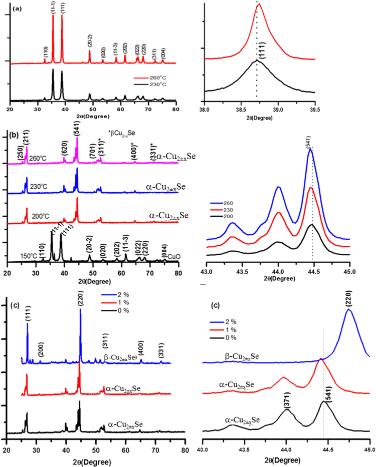
Effects of solvent composition, reaction temperature and doping of silver on size, shape, morphology, and cation/anion ratio of copper oxide/selenide NCs are investigated. Fig. 1 demonstrates XRD patterns of as-synthesized copper oxide/copper selenide NCs under different experimental conditions. Use of double distilled water as a solvent at a given reaction temperature in the range of 150–260 °C produces CuO nano/microparticles where the degree of crystallinity and crystalline size tend to increase with reaction temperature (Fig. 1(a)). Scherrer formula (; where λ = 1.54056 is X-ray line from Cu-Kα source, β is full width at half maximum in radian and θ is half of the peak center) for (111) plane results for crystalline size around 10.56 and 18.14 nm for the copper oxide NCs produced at reaction temperatures of 230 and 260 °C, respectively. This means that the use of water as a solvent does not provide a suitable thermodynamic condition for the reaction between CuO and SeO2 powders needed to synthesize Cu2±xSe NCs.
Fig. 1.
X-ray diffraction patterns from as produced powder samples (a) S2 (230 °C) and S3 (260 °C) samples of CuO (left) along with larger angle shift in (111) peak position (right) at higher temperature, (b) S4 (150 °C), S5 (200 °C), S6 (230 °C) and S7 (260 °C) samples of Cu2±xSe nano/micro-powders (left) along with smaller 2θ shift in (541) peak with increase in reaction temperature (right), and (c) S6 (0%), S8 (1%) and S9 (2%) Ag doped Cu2±xSe (left) and enlarged view of diffraction peaks in the 2θ range of 43–45°.
XRD data of powder samples (S4-S7), hydrothermally produced from a mixture of water and EG as a solvent and PVP as a stabilizing agent at a constant reaction temperature in the range of 150–260 °C, is shown in Fig. 1(b) along with the corresponding magnified view in the right column. At 150 °C reaction temperature (S4), the EG and water mixture also produces CuO nanocrystals with almost 10.5 nm crystalline size corresponding to (111) plane. At higher reaction temperatures in the range of 200–260 °C, CuO and SeO2 powders in water/EG mixtures produce α-Cu2±xSe nano/microcrystals (JCPDS 47-1448), where cation/anion ratio, size, shape and morphology are tuned by reaction temperature. It is interesting to note that for the same amount of reactants in the reaction mixture, one can tune density of copper vacancy and hence lattice distortion and carrier concentration simply by tuning reaction temperature [12]. We can clearly see that with the increase of reaction temperature, the diffraction peak corresponding to (541) plane shifts towards smaller 2θ values demonstrating an increase of copper to selenium ratio [28]. At 230 °C Cu/Se ratio is very close to stoichiometric copper selenide with minimum distortion in the lattice (JCPDS 47-1448), however for higher (260 °C) and lower (200 °C) reaction temperatures, cation to anion ratios are respectively larger and smaller relative to the stoichiometric value.
We selected the water/EG mixture as solvent with PVP as a stabilizer and 230 °C reaction temperature for the addition of 1% and 2% w/w of AgO into the reaction mixture by maintaining amounts of copper oxide and selenium oxide at constant values. Doping of copper selenide with 1% Ag retains its α phase (Fig. 1(c); red curve). However, shift towards the lower 2θ value demonstrates increase of cation density in the α-Cu2±xSe lattice. Further increase of Ag concentration upto 2% established a suitable thermodynamic condition that transferred copper selenide NCs from α to β phase (JCPDS 47-1448) without any post-processing such as thermal treatment. In general, transformation of the phase of copper selenide from α to β requires thermal annealing at ∼ 400 K for several hours under vacuum condition [28].
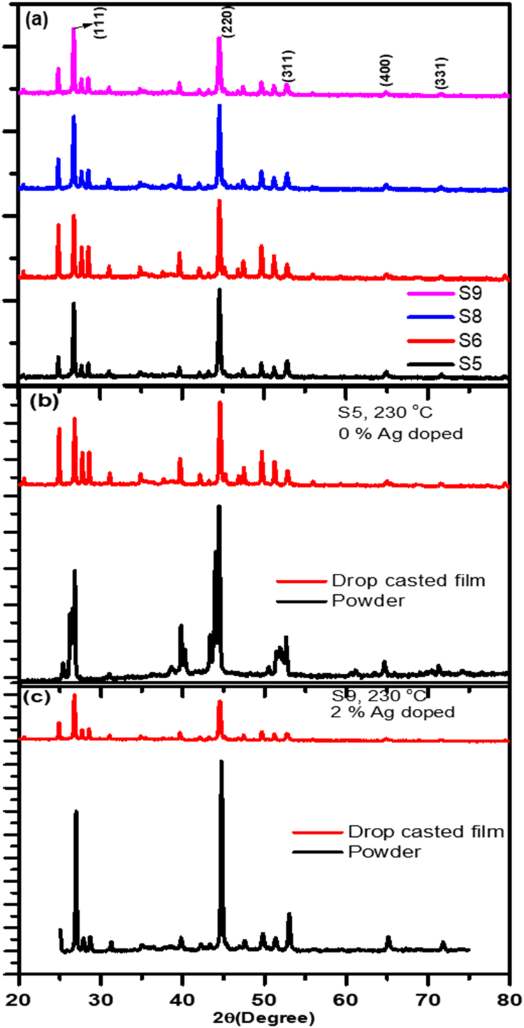
Fig. 2(a) shows XRD patterns of copper selenide NCs (S5, S6, S8 and S9) drop casted on ITO coated glass substrates from the ultrasonic dispersions of corresponding powders. These films have larger ratios of nano to microcrystals as compared to powder samples where micro-crystals are in majority. Prominent XRD peaks are indexed to β phase of copper selenide (JCPDS:06-0680). Comparative diffraction patterns from powder and drop casted films for samples S5 and S9, are presented in Fig. 2(b) and (c), respectively. Based on these investigations, we can conclude that larger sized particles (the majority in powder) are in α crystalline phase for samples S5-S8, while they are in β-phase for sample S9. However, smaller sized particles such as NCs (the majority in drop casted film) are in β-phase for all the samples. The appearance of (311), (400) and (331) diffraction peaks (Fig. 1(b)) of β-Cu2±xSe in powder diffraction of samples S5-S8 also supports the presence of β phase as the trace.
Fig. 2.
X-ray diffraction patterns of (a) Cu2±xSe NCs drop casted on ITO coated glass substrate from ultrasonic dispersions of corresponding powders into acetone. Comparative XRD patterns of as produced powder and drop casted film on ITO coated glass substrate for (b) S5 and (c) S9 samples.
3.2. Electron microscopy, Surface morphology and Compositional investigation
SEM images of NCs produced in double distilled water at 230 and 260 °C reaction temperatures are shown in Fig. S1(a,b) with EDAX spectrum in the inset. Crystals produced at 230 °C are mostly pyramidal shapes, while those obtained from 260 °C reaction temperature have two-dimensional sheet-like structures. EDAX data shows the presence of copper and oxygen only, revealing synthesis of copper oxide rather than copper selenide nanocrystals as shown by XRD measurements in Fig. 1(a).
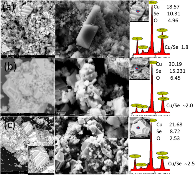
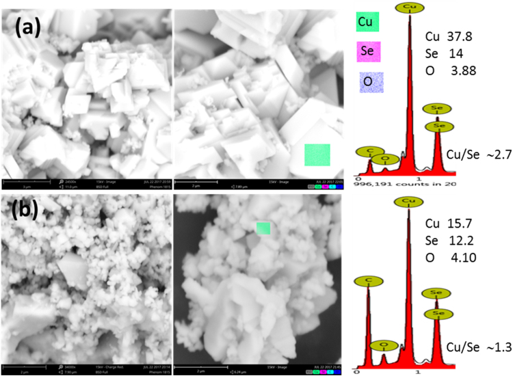
Tuning of reaction temperature under a given synthesis condition can control the rate of reaction and hence size, shape, and composition of NCs. SEM images and EDAX spectra of Cu2±xSe NCs produced in water/EG/PVA solution at 200, 230 and 260 °C reaction temperatures are presented in Fig. 3. With the increase of reaction temperature, not does only the size of individual particles tend to increase, but these particles also get self-assembled into larger size crystals (left column of Fig. 3). The average of EDAX mapping for three different positions of the same crystal and for five different crystals of the same sample gives compositional information of NCs. Interestingly, it is observed that reaction temperature can dictate the elemental composition of final product NCs for the same amount of initial reactants and solvents. The increase of reaction temperature during hydrothermal synthesis increases the copper to selenium (Cu/Se) ratio into the product NCs (right column Fig. 3). On the basis of EDAX investigation, we can say that NCs produced at 200, 230, and 260 °C reaction temperatures are Cu1.8Se, Cu2Se and Cu2.5Se respectively. Here, one can see that nearly stoichiometric copper selenide NCs are produced at 230 °C reaction temperatures, while cation and anion-deficient NCs are produced at 200 and 260 °C reaction temperatures. EDAX elemental investigation supports the lower 2θ shift in (541) peak with increase in reaction temperature (right column Fig. 1(b)). Since we achieved nearly stoichiometric copper selenide at 230 °C reaction temperature, therefore this thermodynamic condition was deliberately chosen for doping of silver atoms into copper selenide lattice. SEM images and EDAX spectra of 1% and 2% w/w Ag doped copper selenide NCs are presented in Fig. 4. As compared to undoped copper selenide (Stoichiometric Cu2Se (Fig. 3(b)), NCs produced with 1% doping of Ag have multifaceted crystal structure, comparatively large particle size (Fig. 4(a); left and central column), and most importantly, they are non-stoichiometric with higher copper to selenium ratios (Cu2.7Se; EDAX spectrum right column Fig. 4(a)). As discussed in Section 3.1, NCs produced with 1% Ag doping retain their α crystalline phase, however, those produced with 2% Ag doping are get transferred to β-phase. SEM images and EDAX data, reveal that not only the phase but the size, shape, morphology, and composition of NCs can be tuned by small amounts of impurity doping. NCs produced with 2% of Ag doping are much smaller in size with an irregular shape (Fig. 4(b)) and have copper deficiency (Cu1.3Se; EDAX spectrum right column Fig. 4(b)).
Fig. 3.
SEM images of Cu2±xSe nano/microcrystals produced in water/ethylene glycol/PVP solvent at (a) 200, (b) 230, and (c) 260 °C reaction temperatures at low resolution (left column), higher resolution (middle column), and corresponding EDAX spectra (right column). Insets in the right column: circle selected on the micron-sized crystals for compositional (EDAX) investigations along with percentage atomic compositions of elements in the tabular form and corresponding copper to selenium (Cu/Se) ratios. The rest of the material is carbon from the conducting adhesive tape used for securing the sample.
Fig. 4.
SEM images of hydrothermally synthesized copper selenide microcrystals into water/ethylene glycol/PVP solvent at 230 °C reaction temperature with (a) 1% and (b) 2% of Ag doping with corresponding EDAX images and elemental mapping. The rest of the material is carbon from the conducting adhesive tape used for securing the sample.
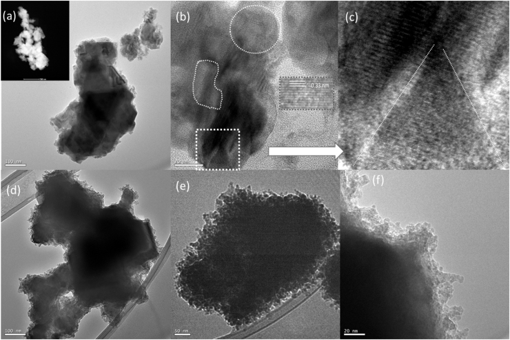
Transmission electron microscopic (TEM) images of copper selenide NCs produced at 200 and 260 °C reaction temperatures are shown in Fig. 5. TEM images (Fig. 5(a–c)) of copper selenide NCs produced in water/PVA/EG solvent at 200 °C reaction temperature (S4) reveals synthesis of a large sized (> 500 nm) single crystal with high degree of crystallinity. Encircled portions and inset (Fig. 5(b)) show lattice fringes at different faces of the crystal presented in Fig. 5(a) revealing high degree of crystallinity of NCs. An enlarged view of one of the face of nanocrystal (highlighted by white square) has pyramidal structure with a high degree of crystallinity, further supports our claim for the synthesis of larger sized single crystals rather than self-assembly or aggregation of smaller sized nanoparticles to build a larger sized crystal. In contrast to this, TEM images of NPs produced at 260 °C reaction temperature (Fig. 5(d–f)) show self-assembly of a large number of smaller (5–20 nm) sized particles as building blocks for larger sized microcrystals. TEM investigations of these two samples disclose that reaction temperature is an important control parameter to tune the strategy for the synthesis of larger sized crystals from smaller sized clusters or atomic/molecular sized entities as building blocks.
Fig. 5.
TEM images of Cu2±xSe nano/microcrystals produced at (a-c) 200, and (d-f) 260 °C reaction temperatures. (a) Low magnification TEM image scale bar 100 nm. (Inset) high angle annular dark field (HAADF) scanning transmission electron microscopy (STEM) image of NCs (b) high magnification; scale bar 20 nm; (Inset) HRTEM shows lattice fringes with an inter-planner spacing of ∼ 0.33 nm, and (c) enlarged view of the squared portion of the image (b). TEM images of copper selenide NCs produced at 260 °C at (d) low; scale bar 100 nm, and (e, f) at higher magnifications; scale bar 50 and 20 nm.
3.3. Reaction temperature and doping induced tuning of Localized Surface Plasmon Resonance (LSPRs) absorption of as-synthesized copper selenide nanocrystals
The interaction of light with nanostructured surfaces is governed by coherent and surface-bound oscillation of free electrons in resonance with the incident electromagnetic field. Due to the localized surface plasmon resonances (LSPRs), nanoparticles exhibit strong electric field enhancement on their surfaces causing enhancements in emission and absorption in molecules in their close vicinity. LSPR absorption, mainly governed by free carrier density (N) of the material, can be used as a probe for the diagnosis and control of electronic conductivity of semiconductors. Blue shift in the LSPR peak position is a widely used tool for size determination of particles with sizes smaller than their quantum confinement (QC) limit. Unlike metals, where LSPRs are only size, shape and ambient environment dependent due to their fixed carrier concentration, semiconductors pose widely tunable LSPRs due to the doping and defect-induced control in their carrier density [29], [30]. Observation of tunable and strong LSPRs in semiconductor NCs such as copper selenide is desirable for efficient optoelectronic and photo-electrochemical properties.
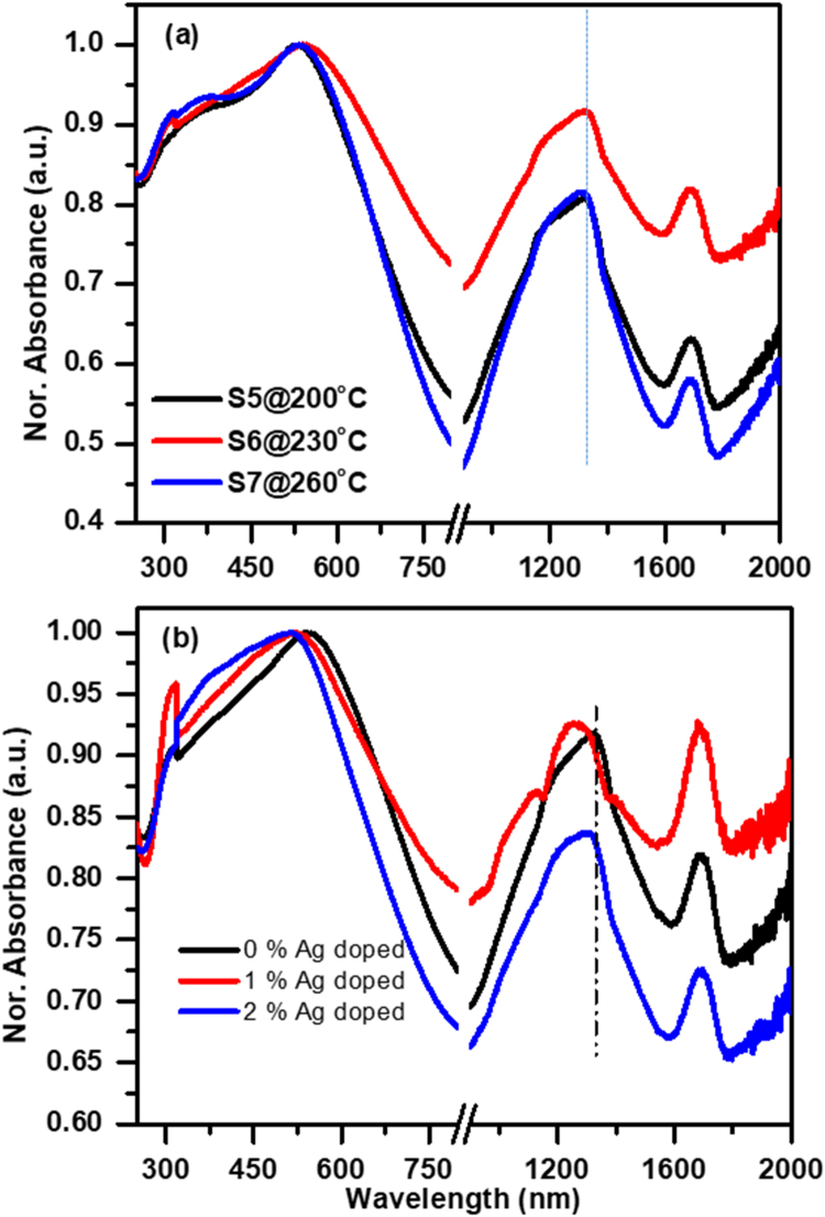
Copper selenide has strong band to band and SPR absorption in the UV–Visible-IR range, therefore it is one of the best materials for solar energy harvesting applications. Absorption spectra of water dispersed copper selenide NCs produced at different reaction temperatures in water/ EG/PVA mixture are shown in Fig. 6(a), while absorption spectra of NPs hydrothermally synthesized using water as solvent at different reaction temperature are presented in Fig. S1(c,d). We ultrasonically dispersed equal amount (0.25 mg/ml) of NCs in double distilled water to make solution for optical absorption measurements. NCs produced at 150 °C reaction temperature in water/EG/PVA mixture has absorption maxima at 370 nm with absorption onset at 870 nm (1.42 eV) corresponding to the direct bandgap of CuO nanoparticles (Fig. S2). Samples produced at higher reaction temperature (200–260 °C) have intense absorption peaks at around 540 nm corresponding to the direct band-gap [12], [15] and fundamental absorption of Cu 2±xSe NPs (Fig. 6(a)). Intense absorption in the broad spectral range of 950–1500 nm with peak center around 1300 nm may be due to the superposition of the much weaker indirect bandgap absorption and pronounced LSPR absorption driven by collective oscillation of the free charge carrier. Therefore, absorption peaks centered at around 1300 nm are Gaussian deconvoluted to extract LSPR absorption and associated properties. The position of the LSPR angular frequency () is related to the free charge carrier density (Nc) through the expression , where is bulk plasma frequency that depends on the density (Nc) and effective mass (mc) of the free charge carrier, and are width of LSPR peak and dielectric constant of the medium, respectively. The position of LSPR angular frequency () and width () are obtained through Gaussian deconvolution of experimentally observed absorption peaks and selecting most intense one (Fig. S3 and Fig. S4) out of all deconvoluted peaks, while mc value for charge carrier in copper selenide NCs is used from Ref. [31]. LSPR peak position (λSP), , and data obtained by Gaussian fitting of experimental absorption spectra are tabulated in Table 2. These data are used for the calculation of bulk plasma frequency () and free charge carrier density (Nc) (Table 2). It is interesting to note that decrease or increase in Cu/Se ratio below or above the stoichiometric value (Cu/Se=2) increases values and hence bulk plasma frequency and free charge carrier density. It is reported that an increase in copper vacancy in Cu2S quantum dots causes blue shift in LSPR peaks and consequently increase in hole density [18]. Similarly, in our case, blue shift in LSPR peak position for Cu1.8Se with respect to that of Cu2Se is due to an increase in hole density. However shorter wavelength shift in LSPR peak position from sample S6 to S8 is attributed to the increase in copper to selenium ratio resulting in the formation of selenium-deficient (Cu2+xSe; n-type) copper selenide NCs and an increase in free electron density. Another absorption peak around 2200 nm (1.3 × 10¹⁴ s−1) (Fig. S5; Supporting information) may be due to the non-spherical shapes of the particles.
Fig. 6.
UV–Visible-NIR absorption plots for as-synthesized nanocrystals produced in the mixture of water/ethylene glycol/ PVP (a) at different reaction temperatures, and (b) with the addition of 0%, 1% and 2% of AgO in the reaction mixture at 230 °C reaction temperature.
Table 2.
Parameters deduced from Gaussian fits of surface plasmon resonance peaks from different α-Cu2±xSe NCs.
| Sample No. | Sample name | λsp(nm) | ωsp(s−1) | γ (s−1) | ωp(s−1) | Nc(cm−3) |
|---|---|---|---|---|---|---|
| S5 | Cu1.8Se | 1246 | 2.41 × 10¹⁴ | 4.64 × 10¹³ | 2.20 × 10¹⁵ | 5.94 × 10²⁰ |
| S6 | Cu2Se | 1253 | 2.39 × 10¹⁴ | 6.36 × 10¹³ | 2.15 × 10¹⁵ | 5.67 × 10²⁰ |
| S7 | Cu2.5Se | 1206 | 2.49 × 10¹⁴ | 4.64 × 10¹³ | 2.24 × 10¹⁵ | 6.16 × 10²⁰ |
| S8 | Cu2.7Se | 1070 | 2.80 × 10¹⁴ | 3.12 × 10¹³ | 2.52 × 10¹⁵ | 7.79 × 10²⁰ |
| S9 | Cu1.3Se | 1225 | 2.45 × 10¹⁴ | 3.4 × 10¹³ | 2.47 × 10¹⁵ | 7.49 × 10²⁰ |
As discussed in Section 3.1, impurity doping causes the change in the crystalline size, induces defect and strain in the lattice, and transfers crystal from α to β phase. Fig. 6(b) shows UV–Vis–IR absorption of undoped (S6), 1% (S8) and 2% (S9) silver doped copper selenide NCs produced at 230 °C reaction temperature. For 1% silver doping, shorter wavelength shift in LSPR peak position relative to the undoped ones, demonstrates an increase in Cu/Se ratio larger than the stoichiometric value, and hence an increase in bulk plasma frequency and free electron density. XRD and SEM investigations showed that 2% doping of Ag into copper selenide lattice converts it from stoichiometric Cu2Se to copper-deficient Cu1.3Se phase that would increase hole density. Observed shorter wavelength shift in the LSPR peak supports XRD and elemental investigations.
3.4. Photoelectrochemical (PEC) measurements
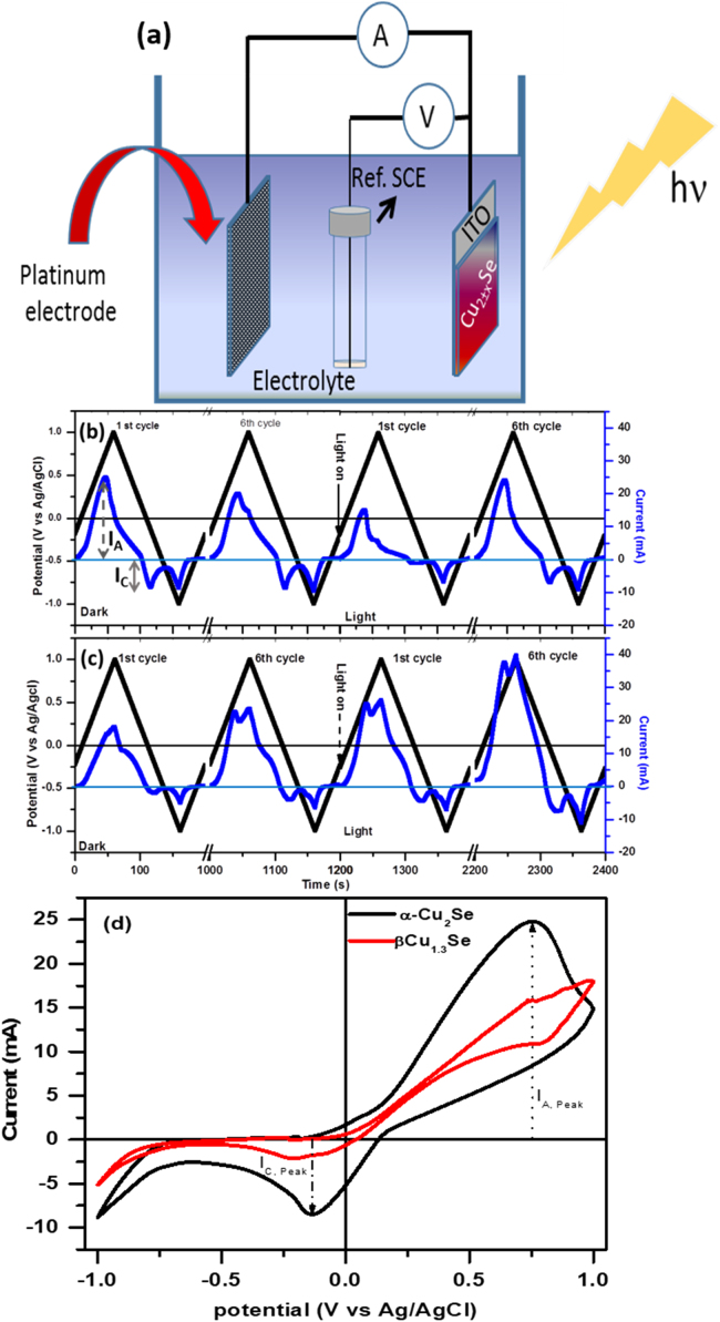
Fig. 7(a) shows a schematic of the three-electrode setup for PEC measurements. Working electrodes, made from stoichiometric Cu2Se (S6) and copper deficient non-stoichiometric β-Cu1.3Se (S9) NCs, were immersed into 0.5 M fresh Na2SO4 electrolyte solution for electrochemical measurements under dark condition and solar light illumination. For each sample, cyclic voltammogram (CV) curves were measured for six cycles in a dark environment followed by six cycles under AM1.5 G solar light illumination with an intentional two-minute interval between the last dark and the first light cycle. Timing diagrams for applied potential (scan @ 20 mV/s) between working and Ag/AgCl reference electrodes and generated electrochemical current between working and counter electrodes are shown in Fig. 7(b) and (c), and in Supporting information Fig. S5. For α-Cu2Se, an anodic (IA) and a cathodic (IC) current peak corresponding to electron transfer during oxidation and reduction processes of test materials are observed before the set positive (+ 1.0 V) and negative (− 1.0 V) potential values, respectively (Fig. 7b,d). Values of peak anodic current (IA) and corresponding potential decrease with the number of cycles in the dark condition. However, under solar light illumination, anodic and cathodic current values, that were much lower for the first light cycles, attain their initial dark values after six light cycles. In contrast to Cu2Se, an electrode made with Cu1.3Se NCs (Fig. 7(c,d)) has no initial anodic current peak corresponding to the oxidation process, but it shows a weak cathodic current peak corresponding to the reduction process in the reverse cycle. However, by increasing the number of cycles under dark conditions as well as under solar light illumination, the values of anodic as well as cathodic currents get increased with the shift in the corresponding potential towards higher values. First cycles of typical cyclic CV curves for electrodes made with Cu2Se and Cu1.3Se NCs under dark are shown in Fig. 7(d).
Fig. 7.
(a) Schematic of three electrode setup for EC and PEC measurements, (b, c) Timing diagram for applied potential (black line) and generated electrochemical current (blue line) for the 1st and the 6th cycles in the dark environment and under solar light illumination for (b) stoichiometric Cu2Se and (c) non-stoichiometric β-Cu1.3Se NCs (Black downward arrows present corresponding times when solar simulator is turned on. There is a two-minute interval (not shown here) between the end of 6th cycle in dark and start of 1st cycle under solar light illumination, and (d) comparative first cycles CV curves for both electrode materials.
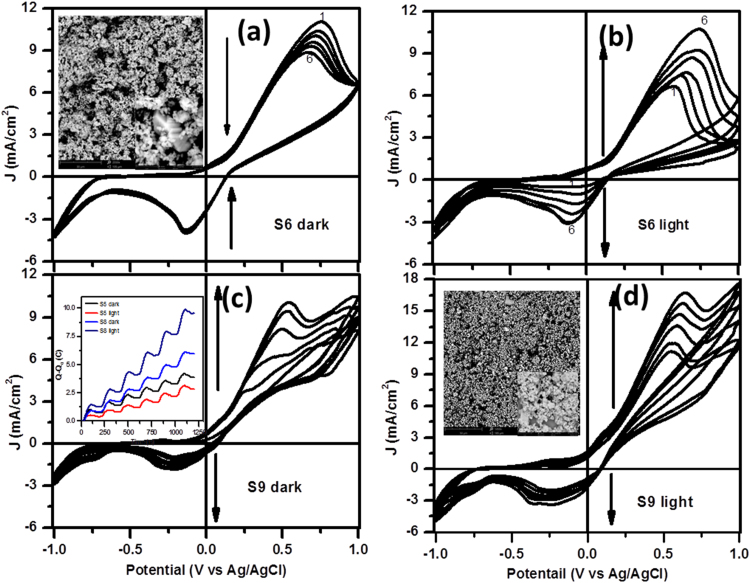
Fig. 8(a) shows six cycles of CV curves for the electrode made with stoichiometric Cu2Se NCs under dark conditions. Each CV curve has an anodic peak around + 0.7 V corresponding to the oxidation of Cu2Se into CuSe (2Cu+ → 2Cu++ + 2e-) and a cathodic peak at − 0.14 V relating to the reduction of CuSe into Cu2Se (2Cu++ + 2e- → 2Cu+). If this redox reaction were reversible, ratios of anodic to cathodic currents would be one. Smaller values of cathodic peak current density (JC) over anodic peak current density (JA), demonstrate that all Cu++ ions produced at the electrode-electrolyte interface during oxidation process, are not reduced back to Cu+ ions, but more than half of them may react with SO4− ions of the electrolyte to make CuSO4 salt in the solution. When the electrode is negatively biased, not only Cu++ from the electrode, but Cu++ from the CuSO4 in the electrolyte also are reduced on the electrode-electrolyte interface to produce almost the initial density of Cu+ ions at the electrode. Ideally, peak height of anodic/ cathodic current density and corresponding oxidation/ reduction potential should be the same for subsequent cycles. However, one can see that with the increase in the number of cycle, anodic current density decreases and oxidation potential shifts towards a lower value (Fig. 8(a)), while cathodic current remains almost constant. This means that all of the copper ions that are released into the electrolyte in the form of CuSO4 is not recycled back to the electrode, therefore, it would degrade with aging.
Fig. 8.
Cyclic Voltammogram (C-V) curves of samples (a, b) Cu2Se and (c, d) β-Cu1.3Se under (a, c) dark and (b, d) light illumination. Insets (a, d): corresponding SEM images of electrodes made of copper selenide nano/microcrystals on ITO coated glass surface. Inset (c): Charge generated on electrode relative to the reference electrode from cycles (1) to (6) for β-Cu2Se and β-Cu1.3Se under dark and one sun enabled solar illumination.
When the solar simulator is turned on (Fig. 8(b)) after two minutes since the completion of sixth dark CV cycle, peak anodic current density (6.6 mA/cm2) for the first cycle under light illumination is much lower than the corresponding value (8.8 mA/cm2) for sixth cycle under dark environment. It shows that even under unbiased conditions, electrode materials interact with electrolyte and get degraded. However, under solar light illumination, peak anodic current starts ramping and nearly attains initial (first cycle) value of peak anodic current under dark condition (Fig. 8(b)). In a similar fashion, peak cathodic current density under light illumination starts from a much lower value (0.48 mA/cm2), but increases continuously with the number of cycles and attains its initial peak dark value (3.78 mA/cm2) and reduction potential (− 0.13 V) after six cycles under solar light illumination. The direction of black arrows in each panel presents CV curves with the increase in the number of cycles. It is clear that for the first six cycles in dark conditions, peak anodic current density (Ja) as well as oxidizing potential (Va) decrease with the number of cycles. However, the initial value is recovered after the next six cycles when the solar simulator is turned on. This means that the electrode made with stoichiometric copper selenide NCs has solar light induced self-repairable capabilities.
Fig. 8(c) and (d) show CV curves for electrodes made with 2% Ag doping (S9; Cu1.3Se) under darkness and solar light illumination conditions respectively. For the first CV cycle under dark, the anodic peak is unclear or may have very small oxidizing potential, while cathodic peak appears at a larger value (− 0.22 V) as compared to undoped copper selenide NCs (− 0.13 V). With the increase in the number of cycles, values of anodic and cathodic current densities, as well as oxidizing and reducing potentials, get increased. As compared to Cu2Se NCs, the electrode made with Cu1.3Se NCs has higher reducing (− 0.22 vs − 0.13 V), but much smaller oxidizing (0.54 vs 0.77 V) potentials. Under solar light illumination, peak values of anodic and cathodic current densities as well as oxidation and reduction potential values, increase with the number of cycles. We performed EC measurements in dark, light, dark, light sequences where each of them has six CV cycles.
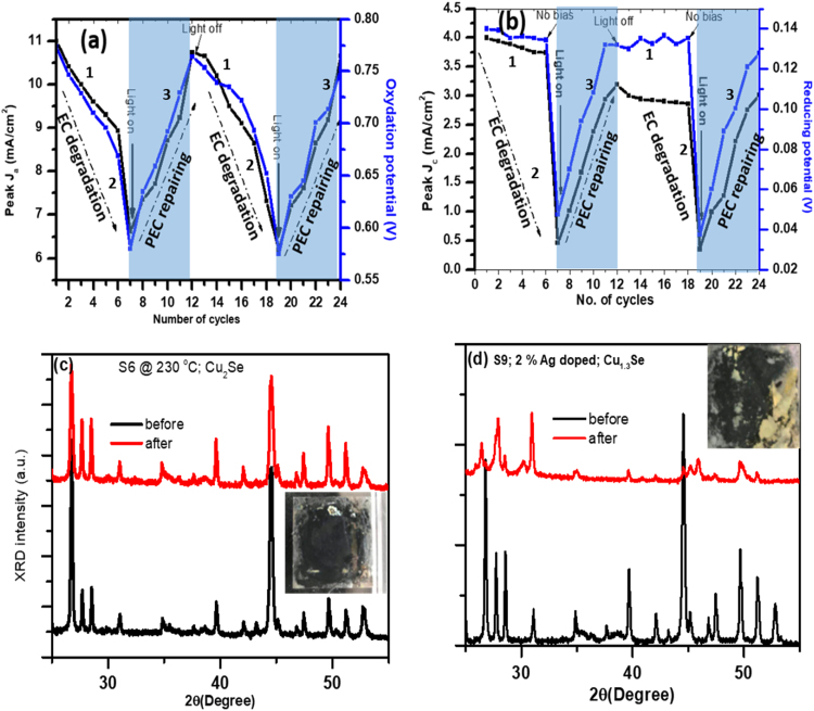
Fig. 9 demonstrates the solar light induced self-repairable capability of an electrode made with stoichiometric copper selenide NCs. Here we can see that with the increase in number of cycles, peak anodic (Fig. 9(a)) and cathodic (Fig. 9(b)) current densities, as well as corresponding potential values, decrease with the number of cycles under the dark condition due to the effective leaching (difference of ions released and recovered back in each cycle) of Cu+ ions into the electrolyte solution. However, under the solar light illumination, anodic and cathodic current densities, as well as redox potential, attain their initial values likely due to the efficient recovery of copper ions from electrolyte solutions to the electrode. We extracted current density and power data from CV curves for better representations of anodic and cathodic current under the dark and solar light illumination conditions to support light induced self-repairable behavior in electrode made of stoichiometric Cu2Se NCs (Fig. S6 and S7: Supporting information). The second set of EC degradation and PEC repairing (Fig. 9(a), (b)) is almost similar to the first set, demonstrating repeatability and durability of light-induced self-repairing mechanism. Leaching of cation from electrode may change structural, compositional and optical properties of electrode material. X-ray diffraction measurement of electrodes made with stoichiometric (S6; Cu2Se) and copper deficient (Cu1.3Se) copper selenide NCs are measured before and after the twenty-four (12 dark and 12 light cycles) EC cycles (Fig. 9(c) and (d)). It is interesting to note that crystallinity and phase of stoichiometric copper selenide remain inherent after PC measurement, while crystallinity of copper-deficient copper selenide NCS has been significantly reduced with the appearance of new peaks. This finding is also supported by direct visualization of the color of the electrodes (insets of Fig. 9(c) and (d)) made from Cu2Se and Cu1.3Se NCs. An electrode made with stoichiometric copper selenide remains dark gray (original color), while more than a 30% portion of the electrode made with copper deficient copper selenide NCs became yellowish after EC measurements showing leaching and oxidation of electrode material. These structural investigations support light-induced self-repairable functionality in electrode made with stoichiometric copper selenide NCs.
Fig. 9.
Demonstration of electrolytic degradation of Cu2Se electrode and its sun-light induced self-repairing. Variations in (a) peak anodic current (Ja) and oxidation potential, and (b) peak cathodic current and reducing potential with the number of cycles under dark and light illumination. Numbers (1), (2), and (3) denote CV ranges for EC measurements in dark (No. of cycles 1–6), unbiased in dark (2 min time interval between 6 and 7) and EC measurements in solar light illumination ((No. of cycles 7–12)). Same is repeated for another EC degradation and PEC repairing cycle. XRD data of electrodes made with (c) stoichiometric (Cu2Se) copper selenide and (d) Cu1.3Se before and after EC and PEC cycles. Insets shows photographs of electrodes after EC and PEC measurements.
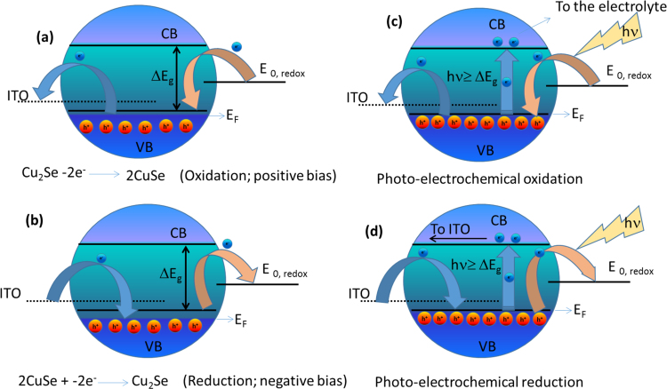
Schematic illustrations for the redox reaction at the electrode-electrolyte interface and resulting charge transfer processes at ITO-copper selenide and copper selenide and electrolyte interfaces are shown in Fig. 10. Copper selenide is a p-type semiconductor with energy levels in the valence band is completely filled up to the fermi-level EF at absolute zero temperature. When ITO is positively biased (first coordinate of CV curves in Fig. 8), transfer of electrons from the valence band (CB) of copper selenide to ITO oxidizes it from Cu2Se (Cu+) to CuSe (Cu++) (Fig. 10(a)) to generate an anodic current. With the increase of positive electrode potential, the number of electrons that are being transferred from copper selenide to ITO increases and attains a maximum value at oxidation potential to achieve a peak anodic current. At this point, all Cu+ ions from copper selenide are converted into Cu++ ions, followed by a chemical reaction between Cu++ ions and SO4— ions at the electrode-electrolyte interface to make CuSO4 salt. In the reverse scan (Fig. 10(b)), electrons are transferred from ITO to the VB of copper selenide to reduce electrode material from Cu++ ions to Cu+ ions along with conversion and transfer of Cu++ ions from electrolyte to the electrode. For electrochemical (EC) reactions in the dark, all Cu++ ions that were converted into CuSO4 through chemical reaction during positive cycles are not converted back into Cu+ ions, therefore the electrode might get corrode with time. However, for PEC under solar light illumination, photons with energy larger than the band gap (hν ≥ Eg) of copper selenide, generate an electron in the conduction band and a hole in the valence band (Fig. 10(c,d)). With the increase of carrier density (hole in the VB) through solar light illumination, we assume that all Cu++ ions from the electrolyte are attracted and reduced to Cu+ to self-repair the electrode surface. From these observations, we can conclude that successive EC reactions in the dark and under solar light illumination conditions might be used for self-repairing, thus dilating the life-time of electrode materials in electrochemical cells and supercapacitors.
Fig. 10.
Schematic illustrations of charge transfer mechanisms at electrode-electrolyte interface during (a, c) oxidation and (b, d) reduction processes in (a, b) the dark environment and (c, d) under solar light illumination.
4. Conclusion
The effects of reaction temperature and silver doping on the structural, compositional and morphological evolution of copper selenide nanocrystals are presented in this paper. Copper selenide NCs cannot be synthesized by mixing selenium oxide and copper oxide in water in the temperature range of 150–260 °C. However, a mixture of water, ethylene glycol, and PVP will produce Cu2±xSe NCs, where size, shape, and elemental composition of NCs can be tuned by reaction temperature. The copper to selenium ratio in α-copper selenide NCs increases with the increase of reaction temperature and results in Cu1.8Se, Cu2Se, and Cu 2.5Se NCs at 200, 230 and 260 °C reaction temperature, respectively. Silver doping in copper selenide NCs not only changes its elemental composition, but also establishes thermodynamic conditions that transfer crystals from α phase to β phase. At 230 °C reaction temperature, 1% doping of Ag changes chemical composition from stoichiometric Cu2Se NCs to selenium deficient Cu2.7Se NCs while retaining its α-crystalline phase. However, 2% doping of Ag produces copper deficient β-Cu1.3Se NCs. We have studied photo-electrochemical (PEC) performance of electrodes made with either stoichiometric Cu2Se or non-stoichiometric Cu1.3Se NCs, and determined that electrode made with stoichiometric copper selenide has light induced self-repairable properties. Therefore, reaction temperature and doping can be used as effective parameters for tuning elemental composition and defect density in copper selenide NCs for self-repairable electrodes for batteries, supercapacitors, and photo-electrochemical fuel generators. Electrodes made with light-induced self-repairable capability will significantly increase the life of electrochemical devices, batteries/supercapacitors, and fuel cells and hence reduce fuel generation and electrical energy storage costs.
Note
The authors declare no competing financial interest.
Acknowledgements
We acknowledge financial supports from U.S. Army Research Office (ARO; grant no. W911NF-15-1-0319), National Science Foundation (NSF; grant no. IIP-1701163), and the Bill & Melinda Gates Foundation (grant no. OPP1119542).
Biographies

S.C. Singh is currently Scientist at The Institute of Optics, University of Rochester, USA and Associate Professor at Guo’s Photonics Laboratory, CIOMP, Changchun China. He received his Ph.D. degree in 2009 from department of Physics, University of Allahabad, India. Dr. Singh has more than eight years of research experience in the Physics and chemistry of materials and their applications in energy harvesting and storage. Dr. Singh served as main editor for Wiley-VCH book “Nanomaterials; Processing and characterization with lasers” and guest editor for special issues of many journals.

Huiyan Li is an undergraduate student at The Institute of Optics, University of Rochester with major in Optics. She is working as undergraduate research student in physical and chemical processing of nanomaterials for device applications.

Chaonan Yao is a graduate student at Guo's Photonics Laboratory, CIOMP, Changchun China. She is working in the field of plasmonic and metasurface waveguides and measurement of optical properties of materials.

Zhibing Zhan received his Ph.D. degree in Materials Physics and Chemistry from Fujian Institute of Research on the Structure of Matter, Chinese Academy of Sciences. Currently, he is working as a postdoctoral researcher at the Institute of Optics, University of Rochester. His scientific research concentrates on femtosecond laser-matter interactions and functionalizing material surfaces through laser engineering: superhydrophilic and superhydrophobic surfaces; and novel micro/nano-hierarchical architectures by scalable laser-chemical hybrid method.

Weili Yu is working as is Associate Professor at Guo's Photonics Laboratory, CIOMP, Changchun China and interested in functional nanomaterials (including polymer, nanocrystal, metal oxide, carbon materials, and 2D materials, etc.). Dr. Yu is dedicated in studying the optics, semiconductor physics and chemistry of materials for light energy related applications, e.g. photovoltaics, photocatalysis, photodetectors, etc.

Zhi Yu is Assistant Professor at Guo's Photonics Laboratory, CIOMP, Changchun China. Dr. Yu's research interests focus on physical and chemical processing of surfaces and their applications in optical and electrochemical sensing.

Chunlei Guo is a Professor in The Institute of Optics at University of Rochester. He also directs the Guo China-US Photonics Laboratory at CIOMP, China. His research is in the area of laser-matter interactions. His work at Rochester led to the discoveries of a range of highly functionalized materials, which may find a broad range of applications. He is a Fellow of American Physical Society and Optical Society of America. Currently, he serves as the Editor-in-Chief for CRC Handbook of Laser Technology and Applications (2nd Edition).
Footnotes
Supplementary data associated with this article can be found in the online version at doi:10.1016/j.nanoen.2018.07.020.
Appendix A. Supporting information
Supplementary material
References
- 1.〈https://www.epa.gov/〉
- 2.Sutherland J.C. Biological effects of polychromatic light. Photochem. Photobiol. 2002;76:164–170. doi: 10.1562/0031-8655(2002)076<0164:beopl>2.0.co;2. [DOI] [PubMed] [Google Scholar]
- 3.Tarascon J.M., Armand M. Issues and challenges facing rechargeable lithium batteries. Nature. 2001;414:359–367. doi: 10.1038/35104644. [DOI] [PubMed] [Google Scholar]
- 4.Goodenough J.B., Kim Y. Challenges for rechargeable Li batteries. Chem. Mater. 2009;22:587–603. [Google Scholar]
- 5.Mal J., Nancharaiah Y.V., Hullebusch E.D., Lens P.N.L. Metal chalcogenide quantum dots: biotechnological synthesis and applications. RSC Adv. 2016;6:41477–41495. [Google Scholar]
- 6.Gao M.R., Xu Y.F., Jiang J., Yu S.-H. Nanostructured metal chalcogenides: synthesis, modification, and applications in energy conversion and storage devices. Chem. Soc. Rev. 2013;42:2986–3017. doi: 10.1039/c2cs35310e. [DOI] [PubMed] [Google Scholar]
- 7.I. Chung, M.G. Kanatzidis, Metal chalcogenides: a rich source of nonlinear optical materials, Chem. Mater., vol. 26(201), pp. 849–869.
- 8.Chauhan V., Reber A.C., Khanna S.N. Metal chalcogenide clusters with closed electronic shells and the electronic properties of alkalis and halogens. J. Am. Chem. Soc. 2017;139:1871–1877. doi: 10.1021/jacs.6b09416. [DOI] [PubMed] [Google Scholar]
- 9.Vamvasakis I., Subrahmanyam K.S., Kanatzidis M.G., Gerasimos S.A. Template-directed assembly of metal–chalcogenide nanocrystals into ordered mesoporous networks. ACS Nano. 2015;9:4419–4426. doi: 10.1021/acsnano.5b01014. [DOI] [PubMed] [Google Scholar]
- 10.Lin J., Zhang Y., Zhou W., Pantelides S.T. Structural flexibility and alloying in ultrathin transition-metal chalcogenide nanowires. ACS Nano. 2016;10:2782–2790. doi: 10.1021/acsnano.5b07888. [DOI] [PubMed] [Google Scholar]
- 11.Chen X.Q., Li Z., Dou S.X. Ambient facile synthesis of gram-scale copper selenide nanostructures from commercial copper and selenium powder. ACS Appl. Mater. Interfaces. 2015;7:13295–13302. doi: 10.1021/acsami.5b01085. [DOI] [PubMed] [Google Scholar]
- 12.Deka S., Genovese A., Zhang Y., Miszta K., Bertoni G., Krahne R., Giannini C., Manna L. Phosphine-free synthesis of p-Type copper (I) selenide nanocrystals in hot coordinating solvents. J. Am. Chem. Soc. 2010;132:8912–8914. doi: 10.1021/ja103223x. [DOI] [PubMed] [Google Scholar]
- 13.Yang L., Chen Z.G., Han G., Hong M., Huang L., Zou J. Te-doped Cu2Se nanoplates with high average thermoelectric figure of merit. J. Mater. Chem. A. 2016;4:9213–9219. [Google Scholar]
- 14.Xue M.-Z., Zhou Y.-N., Zhang B., Yu L., Zhang H., Fu Z.-W. Fabrication and electrochemical characterization of copper selenide thin films by pulsed laser deposition. J. Electrochem. Soc. 2006;153:2262–2268. [Google Scholar]
- 15.Yue J.-L., Sun Q., Fu Z.-W. Cu2Se with facile synthesis as a cathode material for rechargeable sodium batteries. Chem. Commun. 2013;49:5868–5870. doi: 10.1039/c3cc41934g. [DOI] [PubMed] [Google Scholar]
- 16.Hessel C.M., Pattani V.P., Rasch M., Panthani M.G., Koo B., Tunnel J.W., Korgel B.A. Copper selenide nanocrystals for photothermal therapy. Nano Lett. 2011;11:2560–2566. doi: 10.1021/nl201400z. [DOI] [PMC free article] [PubMed] [Google Scholar]
- 17.Zhao Y., Pan H., Lou Y., Qiu X., Zhu J., Burda C. Plasmonic Cu2−xS nanocrystals: optical and structural properties of copper-deficient copper(i) sulfides. J. Am. Chem. Soc. 2009;131:4253–4261. doi: 10.1021/ja805655b. [DOI] [PubMed] [Google Scholar]
- 18.Luther J.M., Jain P.K., Ewers T., Alivisatos A.P. Localized surface plasmon resonances arising from free carriers in doped quantum dots. Nat. Mater. 2011;10:361–366. doi: 10.1038/nmat3004. [DOI] [PubMed] [Google Scholar]
- 19.Zhao L., Wang X., Yun F.F., Wang J., Cheng Z., Dou S., Wang J., Snyder G.J. The effects of Te2− and I− substitutions on the electronic structures, thermoelectric performance, and hardness in melt-quenched highly dense Cu2-xSe. Adv. Electron. Mater. 2011;1:1400015–1400022. [Google Scholar]
- 20.Tyagi K., Gahtori B., Bathula S., Jayasimhadri M., Singh N.K., Sharma S., Haranath D., Srivastava A.K., Dhar A. Enhanced thermoelectric performance of spark plasma sintered copper-deficient nanostructured copper selenide. J. Phys. Chem. Solids. 2015;81:100–105. [Google Scholar]
- 21.Danilkin S.A., Skomorokhov A.N., Hoser A., Fuess H., Rajevac V., Bickulova N.N. Crystal structure and lattice dynamics of superionic copper selenide Cu2−δSe. J. Alloy Compd. 2003;361:57–61. [Google Scholar]
- 22.Ohtani T., Tachibana Y., Ogura J., Miyake T., Okada Y., Yokota Y. Physical properties and phase transitions of β Cu2−xSe (0.20 ≤ x ≤ 0.25) J. Alloy Compd. 1998;279:136–141. [Google Scholar]
- 23.Lesnyak V., Brescia R., Messina G.C., Manna L. Cu vacancies boost cation exchange reactions in copper selenide nanocrystals. J. Am. Chem. Soc. 2015;13:9315–9323. doi: 10.1021/jacs.5b03868. [DOI] [PMC free article] [PubMed] [Google Scholar]
- 24.Gariano G., Lesnyak V., Brescia R., Bertoni G., Dang Z., Gaspari R., Trizio L.D., Manna L. Role of the crystal structure in cation exchange reactions involving colloidal cu2se nanocrystals. J. Am. Chem. Soc. 2017;139:9583–9590. doi: 10.1021/jacs.7b03706. [DOI] [PMC free article] [PubMed] [Google Scholar]
- 25.Lei Y., Chen Z.-G., Han G., Hong M., Zou J. Impacts of Cu deficiency on the thermoelectric properties of Cu2−XSe nanoplates. Acta Mater. 2016;113:140–146. [Google Scholar]
- 26.Luo J., Tilley S.D., Steier L., Schreier M., Mayer M.T., Fan H.J., Gratzel M. Solution transformation of Cu2O into CuInS2 for solar water splitting. Nano Lett. 2015;15:1395–1402. doi: 10.1021/nl504746b. [DOI] [PubMed] [Google Scholar]
- 27.Han A., Zhang H., Yuan R., Ji H., Du P. Crystalline copper phosphide nanosheets as an efficient janus catalyst for solar water splitting. ACS Appl. Mater. Interfaces. 2017;9:2240–2248. doi: 10.1021/acsami.6b10983. [DOI] [PubMed] [Google Scholar]
- 28.Yang L., Chen Z.-G., Han G., Hong M., Zou J. Impacts of Cu deficiency on the thermoelectric properties of Cu2-XSe nanoplates. Acta Mater. 2016;113:140–146. [Google Scholar]
- 29.Agrawal A., Johns R.W., Milliron D.J. Control of localized surface plasmon resonances in metal oxide nanocrystals. Annu. Rev. Mater. Res. 2017;47:1–31. [Google Scholar]
- 30.Kriegel I., Scotognella F., Manna L. Plasmonic doped semiconductor nanocrystals: properties, fabrication, applications and perspectives. Phys. Rep. 2017;674:1–52. [Google Scholar]
- 31.Mansour B.A., Demian S.E., Zayed H.A. Determination of the effective mass for highly degenerate copper selenide from reflectivity measurements. J. Mater. Sci.: Mater. Electron. 1992;3:249–252. [Google Scholar]
Associated Data
This section collects any data citations, data availability statements, or supplementary materials included in this article.
Supplementary Materials
Supplementary material


