Abstract
A potentiostat circuit for the application of bipolar electrode voltages and detection of bidirectional currents using a microelectrode array is presented. The potentiostat operates as a regulated-cascode amplifier for positive input currents, and as an active-input regulated-cascode mirror for negative input currents. This topology enables constant-potential amperometry and fast-scan cyclic voltammetry (FSCV) at microelectrode arrays for parallel recording of quantal release events, electrode impedance characterization, and high-throughput drug screening. A 64-channel FSCV detector array, fabricated in a 0.5-μm, 5-V CMOS process, is also demonstrated. Each detector occupies an area of 45 μm × 30 μm and consists of only 14 transistors and a 50-fF integrating capacitor. The system was validated using prerecorded input stimuli from actual FSCV measurements at a carbon-fiber microelectrode.
Keywords: CMOS potentiostat, bidirectional current, VLSI detector array, fast-scan cyclic voltammetry (FSCV), quantal release, microelectrode arrays, high-throughput drug screening, electrode impedance characterization, dopamine detection
I. INTRODUCTION
NEURONS, the fundamental units of the nervous system, communicate with each other via a chemical signaling process mediated by the storage and release of neurotransmitters, a set of biomolecules that act as chemical messengers to regulate neuronal function and behavior [1]. Neurons store high concentrations of these biomolecules in small membranebound secretory vesicles attached to the inside of the presynaptic plasma membrane. When the presynaptic terminal is electrically stimulated, the vesicles fuse with the plasma membrane through a process called exocytosis, releasing the vesicle contents into extracellular space [2]. Neurotransmitter release from a single vesicle is termed quantal release. The number of biomolecules expelled in a quantal release event is the quantal size [3]. Quantal release has been the subject of extensive medical research because some of the underlying molecular mechanisms mediating exocytosis are still not fully understood. A better understanding of properties such as the quantal size and the frequency and time course of quantal release events is necessary for the discovery and development of new therapeutic drugs that modulate these properties.
Several recording techniques have been used to investigate the properties of quantal release events and their modulation. Constant-potential amperometry (CPA) [4], [5] at a polarizable working electrode is one of the prevalent techniques. Typically, a carbon-fiber microelectrode (CFM) is used as the working electrode due its chemically inert properties, small dimensions (5–20 μm diameter), and thus low noise, allowing high bandwidth recording [6].
In CPA at a CFM, the electrode is held at a positive potential (0.6–0.7 V) with respect to a silver/silver-chloride (Ag|AgCl) reference electrode. Neurotransmitters and hormones from the catecholamine family, such as dopamine and its conversion products adrenaline and noradrenaline, easily oxidize when they come in contact with the surface of the CFM, releasing two electrons each in the process [7]. The resulting electron transfer is then measured as a transient current. Thus, a single exocytotic event such as catecholamine release from chromaffin cells or dopamine release from dopaminergic neurons can be measured as an amperometric current spike, with high precision and high temporal resolution using amperometry. Integration of the transient current spike yields the total charge, from which quantal size can be calculated.
However, CFM recording techniques have their limitations being only capable of measuring quantal release events from a single cell at a time. Each experiment is time-consuming and laborious, requiring precise manual positioning of the CFM adjacent to an individual cell that releases neurotransmitters. Thus, CFM recordings are not suitable for drug screening, an application that requires a statistically significant set of measurements from a large number of cells to obtain conclusive evidence on the effect of a drug on quantal release.
Microelectrode arrays (MEAs) have recently emerged as a viable candidate to replace CFMs as the working electrode mainly because the microfabrication and surface modification techniques involved in the production of MEAs not only provide better reproducibility than traditional CFM fabrication methods but also facilitate batch fabrication of the electrodes [8], [9]. Surface-patterned planar MEAs using noble metals such as gold and platinum and other materials have recently been applied to measure quantal release events from single cells [10]. Scalable arrays incorporate CMOS potentiostats with on-chip electrodes for parallel recordings from large numbers of cells [11]–[14].
Proper functionality of electrochemical electrodes is generally assessed by cyclic voltammetry (CV), in which the voltage applied to the microelectrode is not held constant but instead is ramped from −0.5 V to +1.0 V and back from +1.0 V to −0.5 V (vs. Ag|AgCl). The resulting current reflects the electrode impedance and thus the basic functionality of the electrode. In addition, test analytes such as ferricyanide, which is reduced to ferrocyanide, forming a well-behaved redox pair [10], as well as other compounds [15], have been used in conjunction with cyclic voltammetry for characterization of the performance of electrochemical electrodes. Such measurements cannot easily be performed with unipolar CMOS chips because they require not only the application of bipolar voltages but also the measurement of bidirectional currents.
Cyclic voltammetry can also be used to distinguish between different electroactive species. Fast-scan cyclic voltammetry (FSCV) has been used to perform such measurements on release events from different cell types [7], [16]. In FSCV at a CFM [17], [18], the electrode potential is typically ramped up and down within 10 ms, and these sweeps, or scans, are repeated every 100 ms. The fast rate at which the voltage changes, or the high scan rate, gives rise to a large background current on which the small faradaic current from the reduction and oxidation (redox) of an electroactive compound is superimposed [19]. To recover the faradaic current, the background current elicited during the absence of the compound is subtracted from the total current (sum of background and faradaic currents) elicited during the presence of the compound through a procedure known as background subtraction [20]. This faradaic component is then plotted versus the applied voltage to yield a background-subtracted voltammogram from which the redox voltages can be extracted to identify the detected compound.
This paper reports a precision bidirectional-current CMOS potentiostat circuit along with a prototype 64-channel VLSI FSCV detector array to accelerate the development and testing of new treatments that modulate the size and the kinetics of quantal release. The detector array provides a five-fold increase in temporal resolution over the unidirectional-current detector array we reported previously in [11], [13].
The remainder of this paper is organized as follows: Section II introduces the architecture of the detector array. Section III details the implementation of the core potentiostat unit along with on-chip timing and read-out blocks. Section IV reports measurement results, Section V provides a discussion, and Section VI concludes this paper.
II. SYSTEM ARCHITECTURE
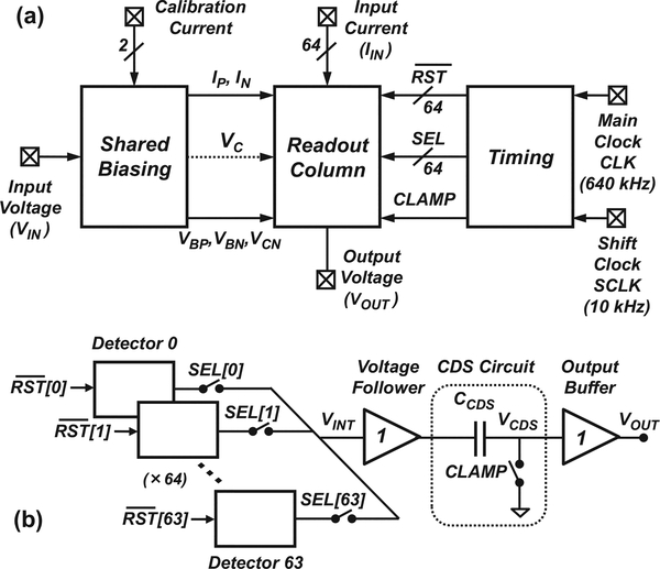
Fig. 1 illustrates a system-level diagram of the 64-channel VLSI FSCV detector array. As shown in Fig. 1a, the array consists of a read-out column with on-chip biasing and timing blocks. As depicted in Fig. 1b, the read-out column consists of a set of 64 detectors that share a common output stage, which in turn consists of a voltage follower, correlated double sampling (CDS) circuit and unity-gain output buffer similar to the one described in [14]. The CDS circuit provides 1/f noise and offset cancellation. The output buffer provides a low output impedance to ensure reliable read-out at a sampling rate of 640 kS/s. The detectors in the read-out column are switched sequentially through a set of select signals from the timing block using a time-division multiplexing technique described in detail in Section III. The output of the read-out column is then fed to an external A/D converter for acquisition.
Fig. 1.
System-level diagram of the FSCV detector array. (a) The system consists of a read-out column along with on-chip biasing and timing blocks. (b) The read-out column contains 64 detectors that share a common output stage consisting of a correlated double sampling (CDS) circuit and an output buffer. Detectors are switched sequentially using time-division multiplexing.
III. CIRCUIT IMPLEMENTATION
A. Bidirectional-Current CMOS Potentiostat
Traditional unidirectional-current potentiostat circuits such as the one described in [21] use a DC offset current to measure bidirectional currents, which not only adds noise (but does not provide gain) to the signal path but also disturbs the charge balance of the electrode-electrolyte interface [22]. The main contribution of this work is a novel potentiostat circuit that enables bidirectional-current measurements from redox processes without use of a DC offset current. The bidirectional-current detection feature doubles the total input current range and enables not only amperometry but also cyclic voltammetry at MEAs.
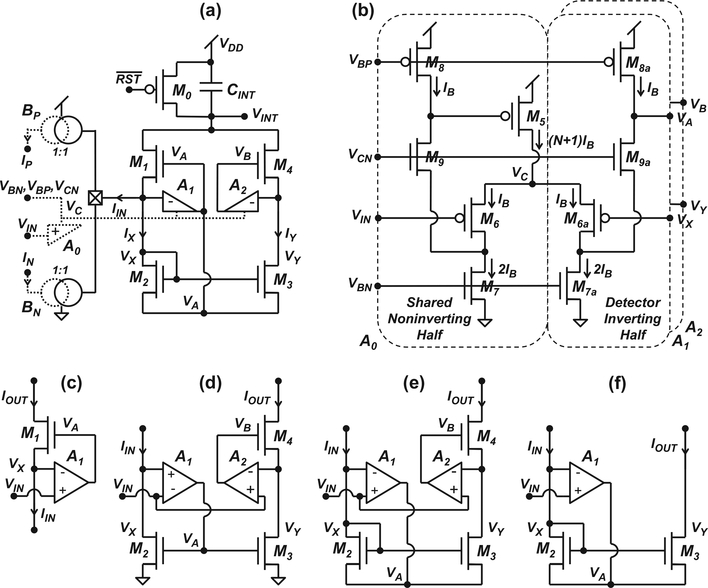
Fig. 2a shows a schematic diagram of the core potentiostat unit, which consists of integration capacitor CINT, switch M0, cascode transistors M1 and M4, mirror transistors M2 and M3, and inverting half amplifiers A1 and A2, that take advantage of the shared amplifier scheme from [14] to minimize the transistor count per detector. Each detector also includes built-in current mirrors BP and BN for calibration currents IP and IN, respectively. The reference half of the calibration mirrors and the shared non-inverting half amplifier A0 (dashed lines) are not part of the detector unit. The core unit was implemented at the cost of only seven additional transistors compared to the one reported in [14]. Fig. 2b shows a schematic diagram of the non-inverting shared half amplifier A0 and the inverting half amplifiers A1 and A2 acting as a folded-cascode amplifier. The amplifier consists of current source M5, input differential pair M6–M6a, load devices M7–M7a and M8–M8a, and cascode devices M9–M9a. Table I lists all device dimensions, bias voltages and capacitor values. Note that M5 in the shared half amplifier carries (N +1)IB where IB is the bias current, and N is the total number of inverting half circuits that share a single non-inverting half amplifier, to minimize the transistor count per detector. In this work, N = 4 because two detector units, and thus two pairs of inverting half amplifiers, share a single non-inverting half amplifier.
Fig. 2.
Schematic diagrams of the (a) bidirectional-current potentiostat unit implemented in this work, (b) shared half amplifier scheme from [14], (c) regulatedcascode amplifier from [14], (d) conventional active-input regulated-cascode mirror from [23], (e) source-driven active-input regulated-cascode mirror from [23], and (f) source-driven active-input current mirror from [24].
Table I.
DETECTOR DESIGN VALUES
| Device | Type | W (μm) | L (μm) | Voltage | Value (V) |
|---|---|---|---|---|---|
| M0 | PMOS | 1.2 | 0.6 | VBN | 1.0 |
| M1–M4 | NMOS | 3 | 3 | VBP | 3.7 |
| M5 | PMOS | 6·(N+1) | 3 | VCN | 1.3 |
| M6, M6a | PMOS | 6 | 3 | VCN | 1.0–2.5 |
| M7, M7a | NMOS | 6 | 3 | Capacitor | Value |
| M8, M8a | PMOS | 3 | 3 | CINT | 50 fF |
| M9, M9a | NMOS | 3 | 3 | CCDS | 2 pF |
The circuit operates as follows: Assuming the Ag|AgCl reference electrode is held at 1.5 V (virtual ground), a voltage ramp (or constant voltage or arbitrary time-varying waveform) is applied to the working electrode at node VIN in the range of 1.0 V to 2.5 V to yield an equivalent range of −0.5 V to +1.0 V vs. Ag|AgCl. A reset signal RST is initially asserted to precharge node VINT to VDD via M0. After the reset signal is de-asserted, node VINT is discharged with the input current through either M1 or M4 for a period of 100 μs. The 100-μs integration time was chosen to provide a 10-kHz sampling rate, which is appropriate to resolve amperometric spikes from chromaffin cells and FSCV data. For positive input current (IIN > 0), which is generally present during the positive slope of the voltage ramp, the circuit operates as the regulatedcascode amplifier from [14], depicted in Fig. 2c. In this case, negative feedback forces VX = VIN and VA > VX, which turns on cascode transistor M1 and allows IIN to flow directly out of CINT into the electrolyte, producing an integration voltage given by
| (1) |
where T0 is the period of the integration phase. For negative input current (IIN < 0), which is generally present during the negative slope of the voltage ramp, the circuit operates as the source-driven active-input regulated-cascode mirror from [23], shown in Fig. 2e. In this case, negative feedback forces the following conditions: VA < VX, which shuts off M1 and turns on M2–M3; VB > VY, which turns on M4; and VX = VY = VIN, which allows all of the input current to flow through M2 and to be mirrored onto M3 with high accuracy, producing an integration voltage identical to (Equation 1) across a wide range of applied voltages. This configuration provides very low systematic transfer error by ensuring the drain-to-source voltages of M2–M3 are identical. Mismatch between M2–M3 certainly results in a random gain error. For this process, the current mismatch varies inversely with the square root of the gate area (Pelgrom’s rule), and NMOS transistors have 2×–3× better current matching for a given size. M2–M3 are NMOS transistors, which is advantageous from a matching viewpoint for a given amount of area. With a drawn area of 9 μm2, the coefficient of variation for M2–M3 is ∼10%. In addition, BP and BN can be used to calibrate the gains of both the positive and negative current measurements, which can further minimize the gain errors.
A detailed noise analysis of the circuit has been previously presented in [14] for the regulated-cascode amplifier mode of operation shown in Fig. 2c, where the input current flows through M1 into the solution (IIN > 0). In this case, the dominant noise sources will be M6–M6a, M7–M7a, and M8–M8a in A0–A1. Similar analysis for the active-input regulatedcascode mirror mode of operation shown in Figs. 2d–2e, where the input current flows through M2 from the solution (IIN < 0), suggests that the relative contributions of the noise sources depends on the electrode impedance, which is difficult to predict with certainty, but the dominant noise sources are likely to be M2–M3, besides M6–M6a, M7–M7a, and M8–M8a in A0–A2. For zero input current (IIN = 0), all amplifiers are shut down and no DC path exists, except for negligible leakage. In this case, the dominant noise source is the sampled kT/C noise from the reset transistor.
Which mode the circuit works in depends on the direction of the input current. The switchover is automatic and, provided that the bandwidth and slew rate of amplifier A1 is high enough compared to the rate of change of the input current, the switchover is smooth. Note that in actual CV or FSCV measurements, when the voltage ramp reaches its maximum value at the end of the positive ramp and starts to decrease at the onset of the negative ramp, the input current also changes rapidly from large positive values to large negative values. The current level at this polarity inversion is strong enough to support the change of VA from a few hundred millivolt above VIN to a few hundred millivolt below VIN. For most cases, the oxidation peaks and reduction peaks will remain unaffected by the switchover as both peaks occur far from the switching point. Also note that the input resistances of the regulatedcascode amplifier and source-driven active-input regulatedcascode mirror are ∼1/(gm1A1) and ∼1/(gm2A1), respectively, where gm1–gm2 are the transconductances of M1–M2, respectively. Because transconductance is proportional to input current, the input resistance of the potentiostat decreases as input current increases in each direction. Simulation results indicate input resistances of 290 kΩ and 588 kΩ at maximum positive and negative input current (±1.5 nA), respectively.
The source-driven topology shown in Fig. 2e was chosen for this work because it does not need compensation, unlike the conventional topology illustrated in Fig. 2d, which requires a compensation scheme that depends on the value of the input current and that becomes impractical for low input current values. Since the output of A1 drives the low-impedance source of M2, and since diode-connected M2 acts as a noninverting passive device, the source-driven topology behaves as a stable single-dominant-pole system that is linear over a wide range of input currents regardless whether the transistors operate in either strong or weak inversion [24]. The activeinput regulated-cascode mirror shown in Fig. 2e was also chosen because it offers orders-of-magnitude higher output resistance (∼A2gm4ro4ro3) compared to the finite output resistance (∼ro3) of the active-input mirror from [24], shown in Fig. 2f. In addition, the active-input regulated-cascode mirror in this work uses differential-input regulation amplifiers that are less sensitive to process and circuit parameters versus the single-input regulation amplifiers used in the regulatedcascode mirrors described in [22], [25]. The potentiostat in this work also avoids use of two separate integration stages [26], which increase the detector’s real estate.
B. Timing Block
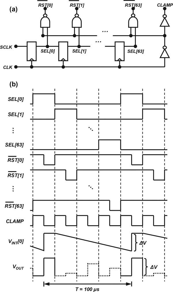
Given the large number of detectors in the array, timedivision multiplexing was implemented to reduce the number of outputs to be sampled off-chip. We limited the number of multiplexed outputs for the read-out column to 64 to avoid the use of a high-frequency on-chip clock, which would add excessive switching noise. Fig. 3 shows the timing scheme used to implement time-division multiplexing of the 64 detectors in the read-out column. Fig. 3a shows a schematic diagram of the timing block, which consists of a 64-stage shift register along with minimal combinational logic. Fig. 3b shows the corresponding timing signals produced by the timing block. The shift register is driven by two external clocks: a 640-kHz main clock, CLK, with 50% duty cycle and a 10-kHz shift clock, SCLK, with ∼1% duty cycle. SCLK is pulsed high briefly every 100 μs. At the positive edge of the main clock, the output of the first D flip flop, SEL[0], goes high to select the output of one of the 64 detectors in the read-out column for one period of the main clock. Consecutive positive edges of the clock activate select signals SEL[1] through SEL[63] in a sequential manner, as seen in Fig. 3b. The process is repeated with each consecutive SCLK pulse. A set of NAND gates is used to derive reset signals [0] through [63] to reset one detector at a time for half of a main clock period. A buffer is used to derive the clamping signal, CLAMP, which is fed to the CDS block in the read-out column.
Fig. 3.
Timing scheme used to implement time-division multiplexing in the read-out column: (a) timing circuit and (b) timing signals.
C. Correlated Double Sampling Circuit
The CDS circuit depicted in the dotted frame in Fig. 1b operates as follows. At the end of the integration period for a particular detector, e.g., Detector 0, select signals SEL[0] and CLAMP are asserted, as shown in Fig. 3b. SEL[0] connects the output of Detector 0, i.e., VINT, to the left plate of a 2-pF capacitor CCDS via a voltage follower, while CLAMP grounds the right plate. Thus, the voltage across CCDS at the end of the integration period is equal to VINT, as described by (Equation 1). At the onset of reset, CLAMP is de-asserted first and [0] is subsequently asserted (pulsed low). During this time, the left plate of the CCDS is pulled to VDD while the right plate is left floating. Subtracting VINT, i.e., the voltage previously stored across CCDS, from VDD yields
| 2 |
where VOUT and VCDS are the outputs of the read-out column’s common output buffer and shared CDS block, respectively, as seen in Fig. 1b, and ΔV represents the voltage step in the signal VOUT shown in Fig. 3b, proportional to the input current.
IV. MEASUREMENT RESULTS
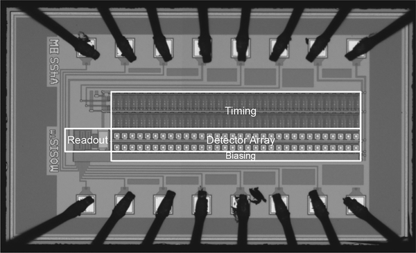
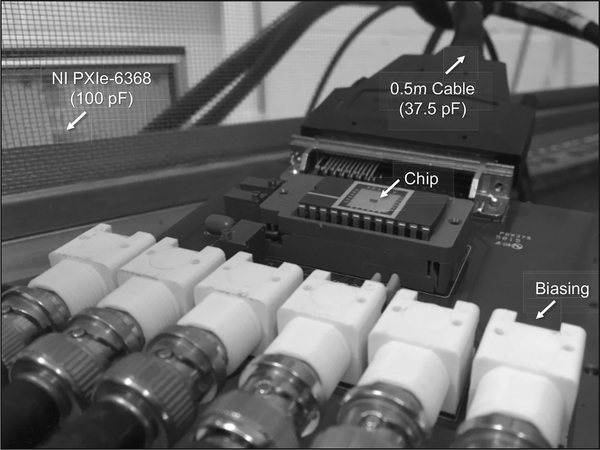
Fig. 4 illustrates a micrograph of the prototype CMOS IC that was fabricated in ON Semiconductor’s 0.5-μm technology. Each potentiostat unit includes a 10 μm × 10 μm glass cut for post-CMOS surface-patterning of the polarizable electrode material, and operates within the typical electrode voltage range of −0.5 V to +1.5 V (vs. Ag|AgCl) for FSCV, at a maximum scan rate of 30 V/s. The area of each potentiostat is 45 μm × 30 μm. The entire system occupies an active area of 276 μm × 1110 μm (excluding pads), and draws 970 μA from a 5-V supply, yielding a total power consumption of 4.85 mW. The heat generated by the chip could be a potential problem for neuron activities [27] and therefore the power budget of the circuit should be carefully examined. The duration of a typical on-chip recording is <10 min. During this time there was no detectable change of temperature in the sample. The sample temperature increased by 0.4 °C within 1 hr of chip operation (measured with a type K thermocouple thermometer, Test Products International Inc., OR). The power is thus low enough to avoid significant heating of the sample even over extended recording times. At zero input current, the RMS noise is 443 fA at 10-kHz bandwidth, which is comparable with the RMS noise of 580 fA at 10-kHz bandwidth for a HEKA EPC10 patch clamp amplifier in medium gain range. For larger positive and negative input currents the maximum RMS noise increases somewhat up to <1 pA and <2 pA, respectively. Fig. 5 shows the measurement setup used for the device characterization and validation experiments, which were carried out inside a grounded Faraday cage to minimize electrical interference. The sampling rate was limited to 10 kHz by the external A/D converter’s input capacitance (100 pF) and the connecting cable’s load capacitance (37.5 pF).
Fig. 4.
Micrograph of the fabricated prototype FSCV detector array IC.
Fig. 5.
Measurement setup used for device characterization and validation.
Table II summarizes the measured performance of the fabricated chip. Table III compares the performance of the chip against that of recently published voltammetric detector arrays. Notably the chip presented here features orders of magnitude smaller detector footprint compared to previous work. The small area of the working electrode enables a reduced double layer capacitance at the electrode-solution interface, and therefore a decreased background current. The advantage is that with a small background current, the maximum input range required is much smaller compared to previous work with large detector area, and the RMS noise is also reduced by orders of magnitude. In a real CV or FSCV measurement from live cells, the amounts of neurotransmitters released from individual vesicles are very small (104–107 molecules) [32], and therefore minimal noise is critical for identifying activity from the cells. The small RMS noise enables on-chip amperometry measurements which typically have peak currents of 1–100 pA [32]. The chip presented in this work also has the potential of performing simultaneous amperometry and FSCV measurements, which can provide more detailed and precise information about cell exocytosis events.
Table II.
SUMMARY OF MEASURED PERFORMANCE
| Conversion Rate | 10 kS/s |
| Input Current Range | ±1.5 nA |
| Input RMS Noise | 443 fA (10-kHz BW) |
| Detector Pixel Power | 13.5 μW |
| Detector Array Power | 0.97 mW |
| Readout Stage Power | 1.80 mW |
| Timing Block Power | 0.95 mW |
| Shared Biasing Power | 1.13 mW |
| Total Chip Power | 4.85 mW |
| Detector Pixel Area Total Chip Area* Supply Voltage |
45 μm × 30 μm 276 μm × 1110 μm 5.0 V |
| Process | 0.5-μm CMOS |
* includes 64-detector array plus readout, timing, and biasing overhead
Table III.
PERFORMANCE COMPARISON OF VOLTAMMETRIC DETECTOR ARRAYS
| This work | [27] | [28] | [29] | [30] | [31] | |
|---|---|---|---|---|---|---|
| Process (μm) | 0.5 | 0.5 | 0.35 | 0.35 | 0.18 | 0.065 |
| Supply Voltage (V) | 5.0 | 5.0 | 3.3 | 3.3 | 1.8 | 1.8 |
| Pixel Count | 64 | 100 | 1,024 | 1 | 200 | 4 |
| Pixel Power (μW) | 13.5 | 21 | – | 9,300 | 12.1 | 36 |
| Pixel Area (mm2) | 0.001 | 0.06 | 0.01 | 0.6 | 0.03 | 0.045 |
| RMS Noise (pA) | 0.443† | 7.2 | 0.540 | 120‡ | 0.480 | 50 |
| Bandwidth (kHz) | 10 | 11.5 | 0.13 | 7 | 0.110 | 10 |
| Input Range (nA) | ±1.5 | ±110 | ±1 | ±300 | ±0.2 | ±2,560 |
| Sweep Rate (V/s) | 30 | 0.04 | 0.1 | 0.095 | 2.8 | 400 |
| Cyclic Voltammetry | Yes | Yes | Yes | Yes | Yes | Yes |
| Amperometry | Yes | – | – | Yes | Yes | – |
open-input measurement
calculated from given information
A. Device Characterization
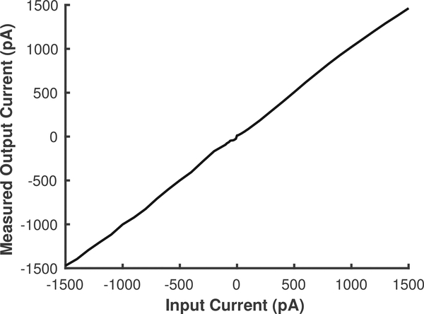
To test the static linearity of the potentiostat, the input current was linearly swept in the range of ±1.5 nA in steps of 10 pA using a Keithley 236 DC current source. Fig. 6 shows the measured output current for positive and negative input currents ranging from 10 pA to 1.5 nA.
Fig. 6.
Measured static linearity of the potentiostat circuit for negative and positive input currents in the range of 10 pA to 1.5 nA.
B. Device Validation
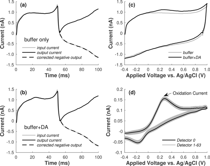
The chip is intended for cyclic voltammetry measurements with on-chip electrodes. Since it was not possible to connect external electrodes to the on-chip contacts, a separate 30-V/s FSCV recording with a CFM was performed to generate a realistic voltammetry current waveform that was used to validate bidirectional current detection with a fabricated chip. CFMs were fabricated from 5-μm diameter carbon fibers as described in [33]. The tip of the carbon fiber was entirely coated with wax and then cut such that only the circular area at the end of the cut fiber was exposed as the working electrode. The area of such a CFM is similar to that of onchip electrodes after post-fabrication [11], [13], which also will be fabricated in the future on the FSCV chip described here. The CFM was immersed into a petri dish filled with a buffer solution containing 140 mM NaCl, 5 mM KCl, 5 mM CaCl2, 1 mM MgCl2, and 10 mM HEPES/NaOH pH 7.3. The electrode potential was swept linearly from −0.45 V to +1.0 V over 50 ms, and back to −0.45 V over the next 50 ms. At the start of the recording, buffer solution supplemented with 1-μM dopamine (DA) was flowed through the dish to replace the DA-free buffer. After two minutes of recording, DA-free buffer was flowed into the dish to replace the DAcontaining buffer. The CFM currents recorded during flow of the DA-free and DA-containing buffer are depicted by the solid gray traces in Figs. 7a–7b, respectively. The slower scan rate, compared to the standard 300-V/s FSCV, was chosen to limit the current amplitude to <1.5 nA, the input range of the on-chip detectors. However, the 30-V/s scan rate is sufficient for on-chip electrode characterization. The main component of the recorded currents is the capacitive background current (Fig. 7a), which changes only slightly due to the additional faradaic DA current (Fig. 7b). This background is due to the ionic double layer capacitance between the electrode surface and the buffer solution, and is roughly proportional to the scan rate [34].
Fig. 7.
(a) Prerecorded input current (solid gray trace) during flow of the dopamine-free buffer, and measured output current before (solid black trace) and after (dashed black trace) offline sign-inversion of the negative data. (b) Prerecorded input current (solid gray trace) during flow of the dopamine-containing buffer, and measured output current before (solid black trace) and after (dashed black trace) offline sign-inversion of the negative data. (c) Measured background voltammograms during flow of the dopamine-free (gray trace) and dopamine-containing buffer (black trace). (d) Measured superimposed background-subtracted cyclic voltammograms for all of the 64 detectors.
The prerecorded input current was fed to the on-chip detectors through BP and BN in Fig. 2a as follows. To avoid excessive capacitive loading from the long cables connecting the Keithley 236 DC current source to the chip, a voltage waveform was applied directly to the diode-connected transistors in each current mirror using discrete components on a custom board with negligible stray capacitance. The applied voltage waveform was calculated from the desired input current waveform based on I-V curves that were obtained for the diode-connected transistors. Positive and negative prerecorded CFM data were applied via BP and BN, respectively. The voltage ramp applied to VIN in Fig. 2a was set to the same voltage ramp used in the 30-V/s FSCV CFM recording. Although a capacitance will form at the electrode-air interface, the resulting current can be safely neglected as the capacitance is extremely small (in contrast to the large capacitance between the electrode and buffer solution). The output of the detector was directly connected to a NI PXIe-6368 external A/D converter.
The solid black traces depicted in Figs. 7a–7b represent the measured output current of a single detector during flow of the DA-free and DA-containing buffer, respectively. It is evident from these traces that the potentiostat in Fig. 2a does not provide the input current directly but rather provides the absolute value of the current due to the use of the same integration capacitor for both positive and negative input currents. To recover the original input current, sign inversion of the negative values of the current was performed offline as follows. First, the zero-crossings of the measured output currents were identified at around t = 53 ms as evidenced by the V-shaped sharp turn of the traces at around this time. Second, a priori knowledge of the shape of the current expected for FSCV was used to confirm that only the values to the right of the zero crossings were the ones that needed sign inversion. The dashed black traces in Figs. 7a–7b represent the corrected output current during flow of the DA-free and DA-containing buffer, respectively. In both cases, the output current after offline sign-inversion of the negative data matches accurately the prerecorded input current. Plotting output current as a function of applied voltage yields the voltammograms shown in Fig. 7c, obtained during flow of the DA-free (gray background trace) and DA-containing (black trace) buffer. The black trace in Fig. 7d represents the corresponding background-subtracted difference voltammogram. The peaks near +0.25 V and −0.15 V (vs. Ag|AgCl) correspond to dopamine oxidation and reduction, respectively. In these test measurements, voltage and current were applied simultaneously to all of the 64 detectors, and the outputs from all 64 detectors were recorded simultaneously. The gray traces in Fig. 7d show the superimposed difference voltammograms from all 64 detectors.
One potential application of cyclic voltammetry would be in the identification of specific transmitters released from individual cells. To resolve cyclic voltammograms during rapidly changing concentrations, as occurs during stimulated release from cells that will be cultured on the chip, a 30-V/s scan rate may be insufficient and should be increased to at least 300 V/s. Due to the 10× higher voltage scan rate, and thus ∼10× larger background current, an electrode capacitance of ∼20 pF is estimated assuming an electrode area of 64 μm2, yielding a background current of ±6 nA for a 300-V/s scan rate. Using ADCs with ultra-small input capacitance for data acquisition, it should possible to increase the sampling rate to 40 kS/s with a reliable output, decreasing the integration time to 25 μs and thus increasing the input current range to ±6 nA. One possibility would be to integrate on-chip ADCs as has been demonstrated for an amperometric front-end chip [35]. For a further reduction in gain, the integration capacitor CINT could be increased to hold more charge during measurement, leading to a lower gain and allowing higher scan rates.
V. DISCUSSION
As mentioned previously in Section IV, the bidirectionalcurrent detector does not measure input currents directly but provides the absolute value instead due to the use of the same integration stage for both negative and positive currents. In the present design, the negative currents were recovered via offline sign inversion. The process was effective given that an identical input current was applied to all of the detectors in the read-out column during measurement. In reality, the input current will vary considerably from detector to detector during actual in vitro measurements. Thus, offline sign inversion becomes impractical for analyzing measurements from all of the 64 detectors in this array. In this case, implementing a zero-crossing detection algorithm using the rules described in Section IV becomes necessary, although not sufficient because the algorithm could miss, in principle, some crossings in the presence of noise. A more robust approach to solve this issue involves generating a binary output signal that reflects the sign of the input current in each detector.
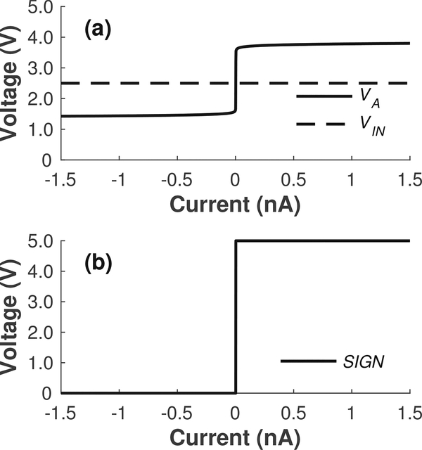
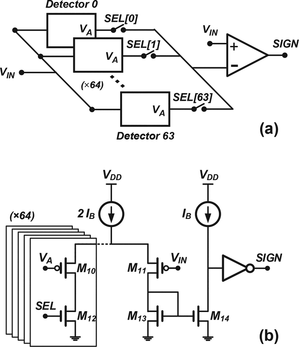
One such implementation, which requires only a minor modification to the existing circuitry, leverages the fact that the output of the regulation amplifier A1 in Fig. 2a, i.e., node VA, is pulled several hundred millivolts higher and lower than the applied voltage VIN for positive and negative input currents, respectively, as illustrated in Fig. 8a. Fig. 9a shows the proposed modification for generating the binary output signal SIGN depicted in Fig. 8b. The technique takes advantage of the same time-division multiplexing and sharedamplifier schemes described in Section II. When the select signal for a particular detector, e.g., Detector 0, goes high for one period of the main clock, a comparator shared by all detectors in a read-out column, compares VIN versus the VA node of that particular detector. Fig. 9b shows a simplified schematic diagram of the shared comparator, which operates as follows. For negative input currents, VA becomes lower than VIN and all of the bias current flows into the detector through M10 and M12. Thus, the drain voltage of M14 is pulled to VDD, which forces the digital output signal SIGN to go low (Fig. 8b). Similarly, for positive input currents, VA becomes higher than VIN and all of the bias current flows instead through M11 into the common current mirror formed by M13–M14. Thus, the drain voltage of M9 is pulled to ground instead, which forces the SIGN to go high (Fig. 8b). The proposed scheme only requires two additional transistors, i.e., M10 and M12, and an extra read-out line per detector, yielding a negligible increase in detector area.
Fig. 8.
Simulation results illustrating the signals used to generate a binary output signal corresponding to the sign of the current. (a) The output of the regulation amplifier A1 in Fig. 2a, i.e., node VA, is pulled several hundred millivolts higher and lower than the applied voltage VIN for positive and negative input currents, respectively. (b) The two signals in (a) can be fed to the comparator in Fig. 9 to generate the desired binary output signal SIGN.
Fig. 9.
(a) Proposed modification to each read-out column in the array to generate a binary output signal corresponding to the sign of the input current. (b) Proposed implementation of the shared comparator shown in (a). The proposed solution only adds two additional transistors and a read-out line per detector for a negligible increase in detector area.
VI. CONCLUSION
In this work, we presented a new CMOS potentiostat circuit topology for application of bipolar voltages and high precision measurements of bidirectional currents. We also introduced a scalable CMOS VLSI potentiostat array for high-throughput drug screening applications. The proposed circuit enables not only amperometry but also FSCV at a MEA for massivelyparallel detection of quantal release events and characterization of electrode impedance, respectively. We demonstrated system functionality through device validation using prerecorded input stimuli. We discussed the potentiostat’s inability to detect the sign of the current, established a methodology for recovering the negative values of the current via a sign inversion procedure, and suggested a minor circuit modification to capture the sign of the current via a binary output signal with minimal area overhead. Ongoing work includes the design and validation of a 16 × 64 FSCV detector array, composed of 16 parallel readout columns, with post-CMOS surface-patterned electrodes for on-chip cell recordings.
ACKNOWLEDGMENT
The authors thank MOSIS for chip fabrication.
This work was supported in part by the National Science Foundation under Grant DGE-0654112 and the National Institutes of Health under Grants R01MH095046 and R43MH109212.
Biography
 Carlos I. Dorta-Quiñones(S’07) received the B.S. degree in electrical engineering and computer science from Massachusetts Institute of Technology (MIT), Cambridge, MA, USA, in 2004, the M.S. degree in electrical engineering from Boston University, Boston, MA, USA, in 2007, and the Ph.D. degree in electrical and computer engineering from Cornell University, Ithaca, NY, USA, in 2014.
During his graduate studies, he held internships at IBM, Mitsubishi Electric Research Laboratories, and Freescale Semiconductor. He is currently with Cavium, Marlborough, MA, where he is working on the modeling, analysis and design of high-speed serial links. His research interests include low-power analog, mixed-signal, and RF integrated circuit design.
 Meng Huang (S’15) received the B.S. degree in materials science and engineering from the University of Illinois, Urbana Champaign, IL, USA, in 2014. He is currently pursuing a Ph.D. degree in materials science and engineering at Cornell University, Ithaca, NY, USA. His research interests include analog and mixed-signal design and device fabrication for biophysics applications.
 John C. Ruelas is an undergraduate student currently pursuing a B.Eng. in electrical and computer engineering at Cornell University, Ithaca, NY, USA. He is currently also with ExoCytronics LLC, Columbia, MO, where he is working on data acquisition hardware and software for electrochemical sensor arrays. He has previously worked at a nonprofit organization where he designed platforms to teach students about various engineering disciplines. His research interests include mixed-signal circuit design, electrophysiology and bioelectronics.
 Joannalyn Delacruz received the B.S. degree in integrative biology, in 2005; the M.S. degree in health education and behavior, with a specialty in adapted education at University of Florida, FL, USA, in 2007; and the Ph.D. degree in pharmacology, neurobiology and behavior from Cornell University, Ithaca, NY, USA, in 2017.
Her projects employ biophysical techniques to investigate the dynamics of exocytosis. Her research interests include neurotransmission of epinephrine and dopamine, and the effects of various therapeutic interventions on learning, motor-learning, behavior and neurophysiological changes.
 Alyssa B. Apsel (S’94–A’02–M’03–SM’10) received the B.S. degree from Swarthmore College, Swarthmore, PA, USA, in 1995, and the Ph.D. degree from Johns Hopkins University, Baltimore, MD, USA, in 2002.
In 2002, she joined Cornell University, Ithaca, NY, USA, where she is currently a professor of electrical and computer engineering. She has authored or coauthored over 90 refereed publications in related fields of RF mixed-signal circuit design, interconnect design and planning, photonic integration with very large scale integration (VLSI), and process invariant circuit design techniques. She holds five patents with several patents pending. The focus of her research is on power-aware mixed-signal circuits and design for highly scaled CMOS and modern electronic systems.
Dr. Apsel has served as an associate editor for various journals, including the IEEE TRANSACTIONS ON CIRCUITS AND SYSTEMS—I: REGULAR PAPERS and IEEE TRANSACTIONS ON CIRCUITS AND SYSTEMS—II: BRIEFS. She was the chair of the Analog and Signal Processing Technical Committee of ISCAS 2011. She was the recipient of a Best Paper Award at ASYNC 2006. She had a MICRO ”Top Picks” paper in 2006. She was the recipient of a college teaching award in 2007 and the National Science Foundation (NSF) CAREER Award in 2004. She was selected by Technology Review Magazine as one of the Top Young Innovators in 2004.
 Bradley A. Minch (M’97) received the B.S. degree (with distinction) in Electrical Engineering from Cornell University, Ithaca, NY, USA, and the Ph.D. degree in Computation and Neural Systems from the California Institute of Technology, Pasadena, CA, USA, in 1991 and 1997, respectively.
Currently, he is Professor of Electrical and Computer Engineering at the Franklin W. Olin College of Engineering, Needham, MA, USA. From 2004 to 2009, he was Associate Professor of Electrical and Computer Engineering at Olin College. From 1997 to 2004, he was an Assistant Professor in the School of Electrical and Computer Engineering at Cornell University. His research interests include low-voltage/low-power analog and digital integrated-circuit design, translinear circuits, log-domain filters, and adaptive floating-gate metal-oxide semiconductor circuits.
Dr. Minch received the IEEE Electron Devices Society’s Paul Rappaport Award in 1996. He received a CAREER award from the National Science Foundation in 2000. He is a member of the Tau Beta Pi, Eta Kappa Nu, and Phi Kappa Phi honor societies.
 Manfred Lindau received the doctoral degree in physical chemistry from the Technical University of Berlin, Berlin, Germany, in 1983.
In 1988, he became Assistant Professor at the Free University of Berlin, Berlin, Germany. From 1992 through 1997, he was an Associate Member of the Max-Planck-Institute for Medical Research, Heidelberg, Germany, and also taught biophysics at the University of Heidelberg, Heidelberg, Germany. He joined the faculty of Cornell University, Ithaca, NY, in 1997, where he is Professor of Applied and Engineering Physics and leads an interdisciplinary research group. Since 2013 he is also head of the Nanoscale Cell Biology Group at the Max-PlanckInstitute for Biophysical Chemistry in Gottingen, Germany. He has developed¨ biophysical techniques for cell and neurobiology including the first perforated patch recordings, improved cell-attached patch capacitance measurements, development of patch amperometry, and the first successful fabrication and application of surface-patterned amperometric electrode arrays. The central goal of his current research is to elucidate the mechanisms of exocytotic fusion and transmitter release. He is active as a consultant in the areas of biophysics, physiology, and cell biology. He is a Founding Member, Member of the Executive Committee and Program Coordinator of the Nanoscale Cell Biology Program at the Science and Technology Center for Nanobiotechnology at Cornell.
In 2003, Dr. Lindau was elected as a Member of the Asian Institute of NanoBioScience and Technology. That same year, he received a Research Award from the Alexander von Humboldt Foundation, Germany, in recognition of his scientific achievements. In 2018, he received the Sir Bernard Katz Award from the Biophysical Society Exocytosis and Endocytosis Subgroup, in recognition of his outstanding contributions as a leader and scientist in the areas of exocytosis and endocytosis. He is a member of the Biophysical Society and the Society for Neuroscience.
Contributor Information
Carlos I. Dorta-Quiñones, Cornell University, Ithaca, NY 14853 USA. He is now with Cavium, Marlborough, MA 01752 USA. (cid2@cornell.edu).
Meng Huang, School of Applied and Engineering Physics, Cornell University, Ithaca, NY 14853 USA (mh2236@cornell.edu)..
John C. Ruelas, School of Applied and Engineering Physics, Cornell University, Ithaca, NY 14853 USA (jcr325@cornell.edu).
Joannalyn Delacruz, School of Applied and Engineering Physics, Cornell University, Ithaca, NY 14853 USA (jbd95@cornell.edu)..
Alyssa B. Apsel, School of Electrical and Computer Engineering,Cornell University, Ithaca, NY 14853 USA (aba25@cornell.edu)..
Bradley A. Minch, Franklin W. Olin College of Engineering, Needham,MA 02492 USA (bradley.minch@olin.edu).
Manfred Lindau, School of Applied and Engineering Physics, Cornell University, Ithaca, NY 14853 USA (ml95@cornell.edu)..
REFERENCES
- [1].Squire LR. Fundamental Neuroscience. Elsevier/Academic Press, 2013. [Google Scholar]
- [2].Kandel ER, Schwartz JH, and Jessell TM. Principles of Neural Science. McGraw-Hill Medical, 5th edition, July 2000. [Google Scholar]
- [3].Edwards RH. The neurotransmitter cycle and quantal size. Neuron, 55(6):835–858, 2007. [DOI] [PubMed] [Google Scholar]
- [4].Chow RH, von Ruden L, and Neher E. Delay in vesicle fusion revealed by electrochemical monitoring of single secretory events in adrenal chromaffin cells. Nature, 356(6364):60–63, March 1992. [DOI] [PubMed] [Google Scholar]
- [5].Wightman RM, Jankowski JA, Kennedy RT, Kawagoe KT, Schroeder TJ, Leszczyszyn DJ, Near JA, Diliberto EJ, and Viveros OH. Temporally resolved catecholamine spikes correspond to single vesicle release from individual chromaffin cells. Proc. Nat. Acad. Sci, 88(23):10754–10758, 1991. [DOI] [PMC free article] [PubMed] [Google Scholar]
- [6].Staal RG, Mosharov EV, Sulzer D. Dopamine neurons release transmitter via a flickering fusion pore. Nat. Neurosci, 7(4):341–346, April 2004. [DOI] [PubMed] [Google Scholar]
- [7].Baur JE, Kristensen EW, May LJ, Wiedemann DJ, and Wightman RM. Fast-scan voltammetry of biogenic amines. Anal. Chem, 60(13):1268–1272, 1988. [DOI] [PubMed] [Google Scholar]
- [8].Zachek MK, Park J, Takmakov P, Wightman RM, and McCarty GS. Microfabricated FSCV-compatible microelectrode array for real-time monitoring of heterogeneous dopamine release. Analyst, 135:1556–1563, 2010. [DOI] [PMC free article] [PubMed] [Google Scholar]
- [9].Zachek MK, Takmakov P, Moody B, Wightman RM, and McCarty GS. Simultaneous decoupled detection of dopamine and oxygen using pyrolyzed carbon microarrays and fast-scan cyclic voltammetry. Anal. Chem, 81(15):6258–6265, 2009. [DOI] [PMC free article] [PubMed] [Google Scholar]
- [10].Gillis KD, Liu XA, Marcantoni A, Carabelli V. Electrochemical measurement of quantal exocytosis using microchips. Pflugers Arch. Eur. J. Physiol, 470(1):97–112, 2018. [DOI] [PMC free article] [PubMed] [Google Scholar]
- [11].Huang M, Delacruz JB, Ruelas JC, Rathore SS, and Lindau M. Surface-modified CMOS IC electrochemical sensor array targeting single chromaffin cells for highly parallel amperometry measurement. Pflugers Arch. Eur. J. Physiol, 470(1):113–123, 2018. [DOI] [PMC free article] [PubMed] [Google Scholar]
- [12].Ayers S, Berberian K, Gillis KD, Lindau M, and Minch BA. Post-CMOS fabrication of working electrodes for on-chip recordings of transmitter release. IEEE Trans. Biomed. Circuits Syst, 4(2):86–92, April 2010. [DOI] [PMC free article] [PubMed] [Google Scholar]
- [13].Kim BN, Herbst AD, Kim SJ, Minch BA, and Lindau M. Parallel recording of neurotransmitters release from chromaffin cells using a 1010 CMOS IC potentiostat array with on-chip working electrodes. Biosens. Bioelectron, 41:736–744, 2013. [DOI] [PMC free article] [PubMed] [Google Scholar]
- [14].Ayers S, Gillis KD, Lindau M, and Minch BA. Design of a CMOS potentiostat circuit for electrochemical detector arrays. IEEE Trans. Circuits Syst. I—Reg. Papers, 54(4):736–744, April 2007. [DOI] [PMC free article] [PubMed] [Google Scholar]
- [15].Zachek MK, Hermans A, Wightman RM, and McCarty GS. Electrochemical dopamine detection: Comparing gold and carbon fiber microelectrodes using background subtracted fast scan cyclic voltammetry. J. Electroanal. Chem, 614(1–2):113–120, 2008. [DOI] [PMC free article] [PubMed] [Google Scholar]
- [16].Pihel K, Schroeder TJ, and Wightman RM. Rapid and selective cyclic voltammetric measurements of epinephrine and norepinephrine as a method to measure secretion from single bovine adrenal medullary cells. Anal. Chem, 66(24), 4532–4537, 1994. [Google Scholar]
- [17].Dorta-Quiñones CI, Wang XY, Dokania RK, Gailey A, Lindau M, and Apsel AB. A wireless FSCV monitoring IC with analog background subtraction and UWB telemetry. IEEE Trans. Biomed. Circuits Syst, 10(2): 289–299, April 2016. [DOI] [PMC free article] [PubMed] [Google Scholar]
- [18].Bozorgzadeh B, Schuweiler DR, Bobak MJ, Garris PA, and Mohseni P. Neurochemostat: A neural interface SoC with integrated chemometrics for closed-loop regulation of brain dopamine. IEEE Trans. Biomed. Circuits Syst, 10(3): 654–667, June 2016. [DOI] [PMC free article] [PubMed] [Google Scholar]
- [19].Robinson DL, Venton BJ, Heien MLAV, and Wightman RM. Detecting subsecond dopamine release with fast-scan cyclic voltammetry in vivo. Clin. Chem, 49(10):1763–1773, 2003. [DOI] [PubMed] [Google Scholar]
- [20].Hayes MA, Kristensen EW, and Kuhr WG. Background-subtraction of fast-scan cyclic staircase voltammetry at protein-modified carbonfiber electrodes. Biosens. Bioelectron, 13(12):1297–1305, 1998. [DOI] [PubMed] [Google Scholar]
- [21].Genov R, Stanacevic M, Naware M, Cauwenberghs G, and Thakor NV. 16-channel integrated potentiostat for distributed neurochemical sensing. IEEE Trans. Circuits Syst. I—Reg. Papers, 53(11):2371–2376, November 2006. [Google Scholar]
- [22].Jafari HM and Genov R. Chopper-stabilized bidirectional current acquisition circuits for electrochemical amperometric biosensors. IEEE Trans. Circuits Syst. I—Reg. Papers, 60(5):1149–1157, May 2013. [Google Scholar]
- [23].Serrano T and Linares-Barranco B. The active-input regulated-cascode current mirror. IEEE Trans. Circuits Syst. I—Reg. Papers, 41(6):464–467, June 1994. [Google Scholar]
- [24].Serrano-Gotarredona T, Linares-Barranco B, and Andreou AG. Very wide range tunable CMOS/bipolar current mirrors with voltage clamped input. IEEE Trans. Circuits Syst. I—Reg. Papers, 46(11):1398–1407, November 1999. [Google Scholar]
- [25].Zeki A and Kuntman H. Accurate and high output impedance current mirror suitable for CMOS current output stages. IEEE Electron. Lett, 33(12):1042–1043, June 1997. [Google Scholar]
- [26].Narula HS and Harris JG. A time-based VLSI potentiostat for ion current measurements. IEEE J. Sensors, 6(2):239–247, April 2006. [Google Scholar]
- [27].Li H, Parsnejad S, Ashoori E, Thompson C, Purcell EK and Mason AJ. Ultracompact microwatt CMOS current readout with picoampere noise and kilohertz bandwidth for biosensor arrays. IEEE Trans. Biomed. Circuits Syst, 12(1):35–46, February 2018. [DOI] [PMC free article] [PubMed] [Google Scholar]
- [28].Rothe J, Frey O, Stettler A, Chen Y, and Hierlemann A. Fully integrated CMOS microsystem for electrochemical measurements on 32 × 32 working electrodes at 90 frames per second. Anal. Chem, 86(13):6425–6432, 2014. [DOI] [PMC free article] [PubMed] [Google Scholar]
- [29].Ghoreishizadeh SS, Taurino I, Micheli GD, Carrara S, and Georgiou P. A differential electrochemical readout ASIC with heterogeneous integration of bio-nano sensors for amperometric sensing. IEEE Trans. Biomed. Circuits Syst, 11(5): 1148–1159, October 2017. [DOI] [PubMed] [Google Scholar]
- [30].Guo J, Ng W, Yuan J, Li S, and Chan M. A 200-channel areapower-efficient chemical and electrical dual-mode acquisition IC for the study of neurodegenerative diseases. IEEE Trans. Biomed. Circuits Syst, 10(3): 567–578, June 2016. [DOI] [PubMed] [Google Scholar]
- [31].Nasri B, Wu T, Alharbi A, Gupta M, RanjitKumar R, Sebastian S, Wang Y, Kiani R, and Shahrjerdi D. Heterogeneous integrated CMOS-graphene sensor array for dopamine detection. 2017 IEEE Int. Solid-State Circuits Conf. (ISSCC), February 2017, pp. 268–269 [Google Scholar]
- [32].Schroeder TJ, Jankowski JA, Kawagoe KT, Wightman RM, Lefrou C, Amatore C. Analysis of diffusional broadening of vesicular packets of catecholamines released from biological cells during exocytosis. Anal. Chem, 64(24):3077–3083, 1992. [DOI] [PubMed] [Google Scholar]
- [33].Berberian K, Kisler K, Fang Q, and Lindau M. Improved surfacepatterned platinum microelectrodes for the study of exocytotic events. Anal. Chem, 81(21):8734–8740, 2009. [DOI] [PMC free article] [PubMed] [Google Scholar]
- [34].Michael DJ, and Wightman RM. Electrochemical monitoring of biogenic amine neurotransmission in real time. J. Pharm. Biomed. Anal, 19(1–2):33–46, 1999. [DOI] [PubMed] [Google Scholar]
- [35].Li H, Boling CS, and Mason AJ. CMOS amperometric ADC with high sensitivity, dynamic range and power efficiency for air quality monitoring. IEEE Trans. Biomed. Circuits Syst, 10(4): 817–827, August 2016. [DOI] [PMC free article] [PubMed] [Google Scholar]


